Electronic band gaps and transport properties in aperiodic bilayer graphene superlattices of Thue-Morse sequence
Abstract
We investigate electronic band structure and transport properties in bilayer graphene superlattices of Thue-Morse sequence. It is interesting to find that the zero- gap center is sensitive to interlayer coupling , and the centers of all gaps shift versus at a linear way. Extra Dirac points may emerge at 0, and when the extra Dirac points are generated in pairs, the electronic conductance obeys a diffusive law, and the Fano factor tends to be 1/3 as the order of Thue-Morse sequence increases. Our results provide a flexible and effective way to control the transport properties in graphene.
pacs:
73.61.Wp, 73.20.At, 73.21.-bGraphene, a potential material with applications that continue to riseNovoselov2004 ; AHCastro2009 ; Peres2010 ; Chen2009 ; Ma2010 ; MZarenia2012 ; LBrey2009 . The monolayer graphene is a semi-metal or zero-gap semiconductor, and the bilayer graphene provides the first semiconductor with a gap that can be tuned externallyZhang2009 . In graphene, the low-energy charge carries behave as massless Dirac fermions near Dirac point (DP), and the resulting linear energy dispersion relation leads to many interesting electronic and optical properties. Recently, motivated by the experimental realization of graphene superlattices (GSLs) JC2008 ; ALVa2008 , enormous theoretical investigations have been done on the GSLs with periodic, qusi-periodic and aperiodic electrostatic potentials or magnetic barriers Park2008 ; LGWang2010 ; PLzhao2011 ; TXMa2012 ; Liang2011 ; MK2011 ; ZhRzh2012 ; MBarb2010 ; XXGuo2011 ; Gong2012 . It is well known that superlattices are vastly used to control the electronic band structure of many conventional semiconducting materials and they have had huge impact on semiconductor physics Tsu2005 ; Cott1989 . In monolayer graphene supperlattice, it has been found that an unusual DP appears in the band structure, and it is exactly located at the energy which corresponds to the zero- gap LGWang2010 ; TXMa2012 . The location of the zero- gap near DP is not only independent on lattice constant but also insensitive to incident angles in contrary with other Bragg gaps, which results in the robust transport propertiesLGWang2010 ; XXGuo2011 ; PLzhao2011 ; TXMa2012 .
In this letter, we investigate the electronic band gaps and transport properties in bilayer graphene superlattices (BLG SLs) of Thue-Morse (TM) sequenceTM . As a typical aperiodic sequence, the TM lattice has been investigated extensively NLiu1997 ; ZCheng1988 ; Luck1989 ; Jiang2005 ; Noh2011 . It is a deterministically aperiodic structure and has a degree of order intermediate between quasi-periodic and disordered system NLiu1997 . Contrary to the result of structure factor, the electron behaviors of TM sequence show that it is more similar to a periodic system NLiu1997 . It is known to have a continuous Fourier transform ZCheng1988 and there is relationship between geometrical characters and their physical properties Luck1989 . In the BLG SLs of TM sequence, it is very important to see that the zero- gap can be tunable by the interlayer coupling . The zero- gap happens in the BLG SLs of TM sequence, resulting in the robust transmission properties different from monolayer GSLs. Moreover, Extra DPs arise and they are dependent on lattice constant.
We consider the electronic structure of BLG with energy and wave vector close to the point, so the one-particle Hamiltonian for BLG is
| (1) |
Here, is the electrostatic potential which only depends on the coordinate , is the interlayer coupling, m/s is the Fermi velocity, and are the momentum operators MZarenia2012 , and , . The wave function is expressed by a four-component pseudospinors . Due to the translation invariance in the direction, the wave function can be rewritten as , m=1,2,3,4. By solving the eigenequation, the wave functions at any two positions to inside the th potentials can be related by a transfer matrix
| (2) |
and
| (3) |
where , , , and . For an -th TM sequence, , and naturally , and so on. Here, () is considered as alternating barrier () with its width (). After a long but straight algebraic deduction, we arrive at the transmission coefficient =, which can be expressed as
| (4) |
is the element of total transfer matrix {X[]}=, where is the total number of layers of GSL. Because the transfer matrix X[] and are both unimodular, it is convenient to derive the recursion relations of the trace map of the -th BLG SLs TM sequence as
| (5) |
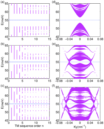
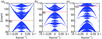
We plot the trace maps for BLG SLs of TM sequence with the order at =0.015 nm-1 in Figs. 1(a-c) and the corresponding band structures are plotted in Figs. 1(d-f), respectively. Figs. 1(a-c) show that a gap opens exactly at =55 meV. The upper and lower bands do not touch together to form a DP at =0 but extra DPs may appear at MBarb2010 , see Figs. 1(e) and 1(f), whose positions are dependent on lattice constant, and we will discuss these in details latter. Since the center of this gap is located at zero-, we may call it zero- gap. One can find that the location of zero- gap center does not shift with lattice constant while other gaps are highly dependent on lattice constant. As illustrated in Fig. 2, the position of the zero- gap changes with the ratio of . It changes from =80 meV, =95 meV to =105 meV with the ratio from 1, 3/2 to 2.
The zero- gap center could be obtained from TXMa2012 . Using to replace here, it is easy to find the energy for =0 as the number of berries and wells is the same. When ,
| (6) | |||||
which is different from the result in the monolayer GSLs TXMa2012 ; Xyafang , due to the existence of . If , Eq. (6) is simplified as
| (7) |
In Figs. 1(b) and 1(c), we can also see that there is no usual DP at =0 but extra DPs emerge, whose locations are determined by the trace =1 Xyafang , expending as
| (8) |
At the normal incident angles (=0), when ==, where is an integer, Eq. (8) always have real solutions, which means the close of zero- gap. For ==, the zero- gap shall close at
| (9) |
At oblique incidence (0), when = =, the extra DPs appear, which locate at
| (10) |
| (11) |
When ==, Eq. (11) can be simplified as
| (12) |
The number of extra DPs can be obtained from Eq. (12).
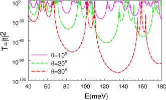
To learn more about the band structures, we study the effect of incident angles on electronic transmission spectrum. From Fig. 3, it is obvious that the position of zero- gap is weakly dependent on incident angle while other gaps change with . Moreover, one can also find that the transmission coefficient decreases as increases, which means that the gaps open much wider.
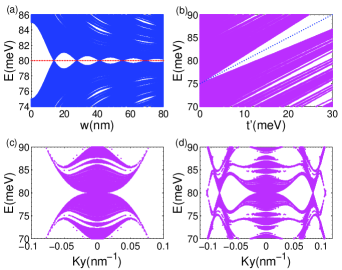
Fig. 4(a) shows that the central position of zero- gap is independent on lattice constant while the other gaps shift greatly. As a result of Eq. (9), the zero- gap is gradually closed and open oscillationally with the increasing at a period of about 13.82 nm for the used parameters. Eq. (9) also indicates that the valence and conduction bands shall touch together periodically, while such touching does not lead to a DPJTwor2006 ; XXGuo2011 , which will be verified further in Fig. 4(c) and 4(d). It is clear that when the gap is closed, the bands touch together but they are not conical near =0, while the extra Dirac points may appear at 0, see Fig. 4(d).
The interlayer coupling is crucial in bilayer graphene and Fig. 4(b) shows its effect on electronic band structure. The dotted blue line denotes the zero- gap center. One can find that all gaps become much wider as increases, especially the zero- gap. When =0, there is no gap, while for 0, the zero- gap opens. The center of all the gaps shift versus at a linear way and the slopes are the same, which means that the band structure will shift as a whole.
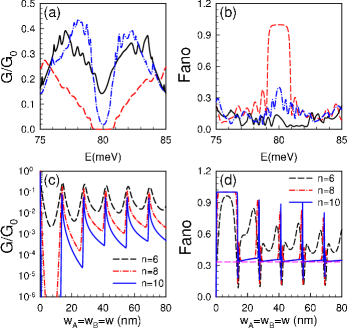
Except for the transmission spectrum, other remarkable transport properties, conductance and Fano factor TXMa2012 ; SDatta1995 ; JTwor2006 ; GF , are demonstrated in Fig. 5. Fig. 5(a) shows that takes its minimum with the Fermi energy in the vicinity of 80meV, but it takes nonzero minimum value at =80meV when the zero- gap closes. However, becomes zero with the Fermi energy in the vicinity of 80meV when the gap is open. We should notice that =80 meV is the zero- gap center. From Fig. 5(b), we can see that the Fano factor becomes much smaller around 80 meV when the zero- gap is closed while it takes its maximum at =80 meV when the gap exists. The valence and conduction bands touch together when the zero- gap is closed (In Figs. 4(c) and 4(d)), but it is not a DP since 1/3 JTwor2006 ; XXGuo2011 . One can also note that takes the value of Poission process shown by the dashed red line in Fig. 5(b), which can be understood by the transmission suppression caused by the energy gap zhu2007 . If energy is fixed at the zero- gap(=80 meV here), and Fano factor are plotted vs the changes of lattice constant in Fig. 5(c) and Fig. 5(d), respectively. One can find that when there are only extra Dirac points with much larger sequence , is proportional to , where is the critical lattice length when the zero- gap closes, see Eq. (9). The corresponding Fano factor is gradually approaching .
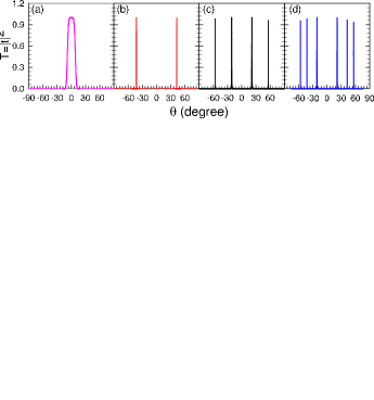
To demonstrate the location of the extra DPs, we plot transmission versus the incident angles of carriers in Fig. 6 where the energy is fixed at 80 meV. One can find that the transmission is perfect at some certain angles, which means extra DPs appear in the band structure when nmXyafang . Extra DPs appear in pairs, and there are more and more pairs of extra DPs as the lattice constant increases, which can be expected from Eq. (12). What’s more, it is easy to get the location and number of extra DPs experimentally.
In summary, we have studied the electronic transport properties in the BLG TM sequence. The zero- gap center is robust against the lattice constant but sensitive to interlayer coupling . When the extra Dirac points are generated in pairs in such structures, the electronic conductance obeys the diffusive law, , and the Fano factor tends to 1/3, as the order of TM sequence increases. These results provide a flexible and effective way to control the transport property in graphene, which is substantial for a lot of graphene-based electronic devices.
This work is supported by NSFCs (Grant. No. 11104014, No. 11274275, No. 61078021, and No. 11374034), Research Fund for the Doctoral Program of Higher Education of China 20110003120007, SRF for ROCS (SEM), and the National Basic Research Program of China (Grant No. 2011CBA00108, and No. 2012CB921602 ).
References
- (1) K. S. Novoselov, A. K. Geim, S. V. Morozov, D. Jiang, Y. Zhang, S. V. Dubonos, I. V. Grigorieva, and A. A. Firsov, Science 306, 666 (2004); K. S. Novoselov, A. K. Geim, S. V. Morozov, D. Jiang, M. I. Katsnelson, I. V. Grigorieva, S. V. Dubonos and A. A. Firsov, Nature 438, 197(2005).
- (2) A. H. Castro Neto, F. Guinea, N. M. R. peters, K. s. Novoselov and A. K. Geim, Rev. Mod. Phys 81, 109 (2009).
- (3) N. M. R. Peres, Rev. Mod. Phys. 82, 2673 (2010).
- (4) X. Chen and J.-W Tao, Appl. Phys. Lett. 94, 262102 (2009).
- (5) T. Ma, F. M. Hu, Z. B. Huang, and H.-Q. Lin, Appl. Phys. Lett. 97, 112504 (2010); F. M. Hu, T. Ma, H.-Q. Lin, and J. E. Gubernatis, Phys. Rev. B 84, 075414 (2011).
- (6) M. Zarenia, P. Vasilopoulos, and F. M. Peeters, Phys. Rev. B 85, 245426 (2012)
- (7) L. Brey and H. A. Fertig, Phys. Rev. Lett. 103, 046809 (2009).
- (8) Y. B. Zhang, T.-T. Tang, C. Girit, Z. Hao, M. C. Martin, A. Zettl, M. F. Crommie, Y. R. Shen and F. Wang, Nature 459, 820 (2009).
- (9) A. L. Vazquez de Parga, F. Calleja, B. Borca, M. C. G. Passeggi, Jr., J. J. Hinarejos, F. Guinea, and R. Miranda, Phys. Rev. Lett. 100, 056807 (2008).
- (10) J. C. Meyer, C. O. Girit, M. F. Crommite and A. Zettl, Appl. Phys. Lett. 92,123110 (2008).
- (11) C. -H. Park, L. Yang, Y.-W. Son, M. L. Cohen, and S. G. Louie, Nat. Phys. 4, 213 (2008).
- (12) P.-L. Zhao and X. Chen, Appl. Phys. Lett. 99, 182108 (2011).
- (13) X.-X. Guo, D. Liu, and Y.-X. Li, Appl. Phys. Lett. 98, 242101 (2011).
- (14) L.-G. Wang and S.-Y. Zhu, Phys. Rev. B 81, 205444 (2010); L.-G. Wang and X. Chen, J. Appl. Phys. 109, 033710 (2011).
- (15) T. Ma, C. Liang, L.-G Wang, and H.-Q. Lin, Appl. Phys. Lett. 100, 252402 (2012).
- (16) Q. F. Zhao, J. B. Gong, and C. A. Muller, Phys. Rev. B 85, 104201 (2012).
- (17) L. Z Tan, C.-H Park, and S. G. Louie, Nano Lett. 11, 2596 (2011).
- (18) M. Killi, S. Wu, and A. Paramekanti, Phys. Rev. Lett. 107, 086801 (2011).
- (19) Z.-R Zhang, H.-Q Li, Z.-J Gong, Y.-C Fan, T.-Q Zhang, Appl. Phys. Lett. 101, 252104 (2012).
- (20) M. Barbier, F. M. Peeters, and P. Vasilopoulos, Phys. Rev. B 81, 075438 (2010).
- (21) R. Tsu, Superlattice to Nanoelectronics (Elsevier, Oxford, 2005).
- (22) Cottam, M. G. Tilley, D. R. Introduction to Surface and Superlattice Excitations(Cambridge Univ. Press, Cambridge, UK, 1989).
- (23) TM sequence, generated by two symbols A and B, follows the inflation rules A AB, B BA, and the successive TM chains are AB, ABBA, ABBABAAB. In Ref.TXMa2012 , some authors of us has inlustrated the way to generate TM squence in detail.
- (24) N.-H Liu, Phys. Rev. B 55, 3543 (1997).
- (25) Z. Cheng, R. Savit, and R. Merlin, Phys. Rev. B 37, 4375 (1988).
- (26) J. M. Luck, Phys. Rev. B 39, 5834 (1989).
- (27) X. Y. Jiang, Y. G. Zhang, S. L. Feng, K. C. Huang, Y. Yi, and J. D. Joannopoulos, Appl. Phys. Lett. 86, 20111 (2005).
- (28) H. Noh, J.-K. Yang, S. V. Boriskina, M. J. Rooks, G. S. Solomon, L. D. Negro, and H. Cao, Appl. Phys. Lett. 98, 201109 (2011).
- (29) Y. Xu, J. Zou, and G. Jin, J. Phys.: Condens. Matter 25, 245301 (2013)
- (30) J. Tworzydlo, B. Trauzettel, M. Titov, A. Rycerz, and C. W. J. Beenakker, Phys. Rev. Lett. 96, 246802 (2006).
- (31) S. Datta, Electronic Transport in Mesoscopic Systems (Cambridge University Press, Cambridge, England, 1995).
- (32) R. Zhu and Y. Guo, Appl. Phys. Lett. 91, 252113 (2007).
- (33) Here and are given by =, =/, where = and =, with denoting the width of the graphene stripe in the direction.