FAU and MPL]Institute of Optics, Information and Photonics, Erlangen Graduate School in Advanced Optical Technologies, Friedrich-Alexander-University Erlangen-Nuremberg (FAU) and Max Planck Institute for the Science of Light (MPL), 91058 Erlangen, Germany \alsoaffiliation[Caltech]Kavli Nanoscience Institute, California Institute of Technology, Pasadena, California 91125, USA Caltech]Kavli Nanoscience Institute, California Institute of Technology, Pasadena, California 91125, USA FAU and MPL]Institute of Optics, Information and Photonics, Erlangen Graduate School in Advanced Optical Technologies, Friedrich-Alexander-University Erlangen-Nuremberg (FAU) and Max Planck Institute for the Science of Light (MPL), 91058 Erlangen, Germany FAU and MPL]Institute of Optics, Information and Photonics, Erlangen Graduate School in Advanced Optical Technologies, Friedrich-Alexander-University Erlangen-Nuremberg (FAU) and Max Planck Institute for the Science of Light (MPL), 91058 Erlangen, Germany Caltech]Kavli Nanoscience Institute, California Institute of Technology, Pasadena, California 91125, USA FAU and MPL]Institute of Optics, Information and Photonics, Erlangen Graduate School in Advanced Optical Technologies, Friedrich-Alexander-University Erlangen-Nuremberg (FAU) and Max Planck Institute for the Science of Light (MPL), 91058 Erlangen, Germany
Functional plasmonic nano-circuits with low insertion and propagation losses
Abstract
We experimentally demonstrate plasmonic nano-circuits operating as sub-diffraction directional couplers optically excited with high efficiency from free-space using optical Yagi-Uda style antennas at . The optical Yagi-Uda style antennas are designed to feed channel plasmon waveguides with high efficiency ( in coupling, total emission), narrow angular directivity () and low insertion loss. SPP channel waveguides exhibit propagation lengths as large as with adiabatically tuned confinement, and are integrated with ultra-compact (), highly dispersive directional couplers, which enable discrimination over with only device loss.
Surface plasmon polariton (SPP) waveguides are uniquely advantaged by their high confinement, allowing for subwavelength integration. This is a requirement for integrating optics with a footprint size that is comparable with electronic circuits - thus enabling plasmonic-electronic hybrid integration, a path that has been repeatedly highlighted as a future key application of plasmonics1, 2, 3, 4.
However, high confinement in plasmonics usually increases loss due to the larger field overlaps with the metal. The second major obstacle to deep subwavelength plasmonics is high insertion loss due to the limited modal field overlap of less-confined waveguide schemes like Si integrated photonics5, 6 or optical fibers7, thus intrinsically limiting the performance of hybrid dielectric-plasmonic circuits8.
Here, we illustrate how in-circuit-loss can be mitigated by restricting strong optical confinement only to components where it is absolutely essential (Fig. 1a), and how insertion-loss can be addressed by coupling light into plasmonic nano-circuits via impedance-matched optimized Yagi-Uda9 style nano-antennas (Fig. 1b,c). Using this platform, we experimentally demonstrate optical directional couplers10, 11 integrated on a micrometer scale that show unusually strong spectral dispersion, a key prerequisite for integrated wavelength division multiplexers.
To implement these device concepts, we use SPP channel waveguides12, 13, which offer maximum confinement14 in a narrow rectangular gap etched a few hundreds nanometers into a metal film. We note that this waveguide geometry does not suffer from optical mode cutoff when scaled down.
By filling the air gap () in the plasmonic waveguide with the substrate material silica () we make the modal field distribution more symmetric (Fig. 1d), therefore eliminating an upper modal cut-off that otherwise prohibits larger waveguide channel widths ( for usual Au channel waveguides), therefore limiting the propagation length to below .
Wherever possible, the connections from one functional plasmonic unit to the next must be bridged with low loss plasmonic waveguides. As the waveguide mode is basically maintained for different gap widths, easy to fabricate adiabatic waveguide tapers can form the transition from highly confining to low loss sections (Fig. 1e).
We experimentally demonstrate that the investigated circuits achieve a propagation length of , while they are still subwavelength with a wave-guide gap width of and that they have an effective refractive index of at with low dispersion.
To reduce insertion loss, each presented nano-plasmonic circuit utilizes at least two connected Yagi-Uda antennas to enhance coupling efficiency from a focused laser beam and to achieve narrow directionality (Fig. 1c). We measured the antenna and waveguide properties spectrally and derive their fundamental properties: efficiency ( in coupling, total emission), directionality () and spectral dispersion.
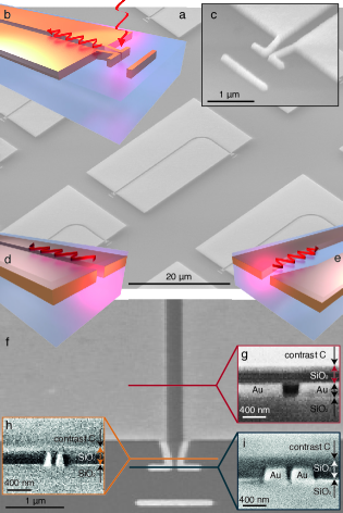
For our experiments, embedded SPP nano-circuits (Figs. 1a and 6b) were fabricated in a two-step process. A thin Au film on a -thin, polished quartz glass substrate was patterned by lift-off with a electron beam lithography system. The designed minimum feature size at the antenna gap (Fig. 1f) was .
Subsequently, flowable spin-on glass (Filmtronics 400F) was spin-coated and baked to form a dielectric cladding layer. Scanning electron microscope images of device cross-sections, cut with a focused ion beam (FIB) at different positions show that the cladding layer fills all gaps, covers the whole structure without cavities (Fig. 1g-i) and forms a smooth surface that is higher than the underlying structures.
The fabricated circuits consistently deviate less than from perfectly rectangular sidewall angles. To investigate the dependence of the optical properties of each circuit component on design parameters, arrays of circuits were fabricated, while systematically varying waveguide length and bend radii (Fig. 1a).
Spectral transmission measurements of each circuit were taken on an optical far-field excitation and imaging setup15 with a supercontinuum light source, spectrally filtered to at FWHM with an acousto optical tunable filter (AOTF) (for sketch and details see supplementary information). A collimated and linearly polarized laser beam was focused by an objective ( dry respectively oil immersion) to a diffraction-limited spot (). The sample was positioned with resolution on a stabilized piezo stage (PI) to couple maximum power into the optical antennas (Fig. 1b).
The whole circuit was simultaneously imaged with or magnification through the excitation objective, a polarization filter and NIR imaging optics on an infrared InGaAs CCD camera (Xenics XS, pixels). With this setup, the linearly polarized emission from output antennas, turned by with respect to the input antenna (Fig. 1a), was imaged with enhanced dynamic range by suppressing the back-reflection from the incident beam with a ratio of up to .
Absolute circuit transmission values were determined by normalizing with the spectral reflectivity of a silica-air interface on the same sample (see supplementary information for details). With additional Fourier imaging, the polarization dependent angular emission pattern of the antennas was analyzed.
For any application, including probing the circuit properties presented here, light has to be coupled into and out of the guided mode of the plasmonic waveguide with highest possible power conversion efficiency.2 Plasmonic antennas are best suited to fulfill this task for exciting channel plasmons from freespace.16, 17
The concept of optical antennas has already been successfully transferred from well-proven radiofrequency technology to the optical and near-infrared with a resulting antenna size in the range.18, 19, 20 Here we apply the macroscopic design concept of Yagi-Uda antennas9 in the near infrared21, 22, 23, 24, 25 and connect them to feed the plasmonic circuits.
For the investigated antennas, the feed element, an approximately long, wide, split Au rod, is centrally illuminated with a focused laser beam () that is polarized parallel to the antenna arms (Fig. 1b,c). This element is driven at its resonance frequency and feeds the wide SPP channel waveguide. An additional non-resonant Yagi-reflector element is placed in a distance of to the feed element to constructively reflect the electromagnetic field back into the waveguide, thus enhancing the in-coupling efficiency.
Our whole design was developed using an iterative particle-swarm-optimization algorithm based on full 3D FDTD simulations while taking into account the limitations of fabrication and real optical material parameters as determined with ellipsometry. As it was found that in-coupling efficiency increases with decreasing size of the antenna gap21, we limited the antenna gap dimension to 80 nm based on fabrication limitations. A taper was added to connect the antenna with a 300-nm-wide low-loss waveguide to minimize impedance mismatch and back reflections.
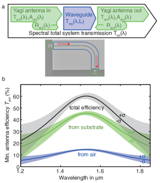
To simplify the experimental analysis of our circuits we attributed lumped properties to each element (Fig. 2a)1. The antennas were assigned a characteristic spectral transmission that represents the ratio of power, which is converted into the waveguide mode for a specific wavelength, a spectral absorption due to Ohmic losses and a reflectivity at the antenna-waveguide connection caused by residual impedance mismatch1,17.
For the waveguides we assigned a length-dependent transmission which is quantified in terms of the propagation length of their supported SPPs. Hence, is separated by multiple measurements over a systematic variation of the waveguide length . In applying this model to our experiments, we furthermore assume that in- and out-coupling antennas had similar, inversion-invariant properties. This is a reasonable approximation as we inject and extract light using the same objective. Hence, the total system transmission is given by
We experimentally measured the spectral system transmission in the range of in steps of , coupling in and out of the circuit from air or through the silica substrate. An ensemble of 20 () different plasmonic nano-circuits was characterized (Fig. 1a), repeated on 4 different samples with the same fabrication settings. Each parameter variation ensemble contained circuits with different total waveguide lengths () and different radii () for the 90° bend that turns the waveguide mode polarization for the emitting antenna.
A systematic analysis of the bend loss over radius demonstrated that bends with offer negligible additional loss compared to the linear waveguide propagation loss, which is comprehensible since the modal effective wavelength difference for those radii is negligible compared to straight waveguides. Hence, we focused our analysis to circuits with a bend radius.
Based on this finding, we fitted the transmissions of the circuits with an iterative two-dimensional least-square fit over the independent variables, wavelength and waveguide length. The antenna transmission was modeled assuming a Lorentzian spectral broadening response,
Under the assumption that dispersive effects of the in- and outcoupling are solely caused by the antenna resonance, we find that the peak wavelength and linewidth are independent of the excitation, whereas the maximum antenna efficiency is higher for excitation from and emission into the substrate than into air due to the refractive index asymmetry of the structure, .
From this fit the spectral propagation length (Fig. 5a, blue curve) and the spectral antenna transmission were determined over all measurements and circuits (few circuits with obvious fabrication errors were excluded from the evaluation). The fit error (standard deviation ), therefore includes statistical errors of both the measurement and fabrication (Fig. 2b). The determined antenna efficiency is a lower limit, as we might not have eliminated all possible sources of losses in the circuit.
The antenna transmission peaks at with a spectral width of , corresponding to a . The spectral peak efficiency of the antennas is from air and from the substrate with minimum statistical error around the peak and increasing error towards the measurement limits of and , where the absolute circuit transmission and the InGaAs camera efficiency decrease.
Keeping the initial assumption that the antenna properties obey optical inversion symmetry, the total antenna efficiency, giving the total emission into air and silica, can be spectrally summated to be , the highest power transmission for a waveguide loaded optical antenna, reported to date.
Validity of the applied transmission analysis is based on the hypothesis that the objective collects all light that is emitted from the Yagi antennas and that a good overlap of the focused exciting beam and the angular emission directionality is achieved.
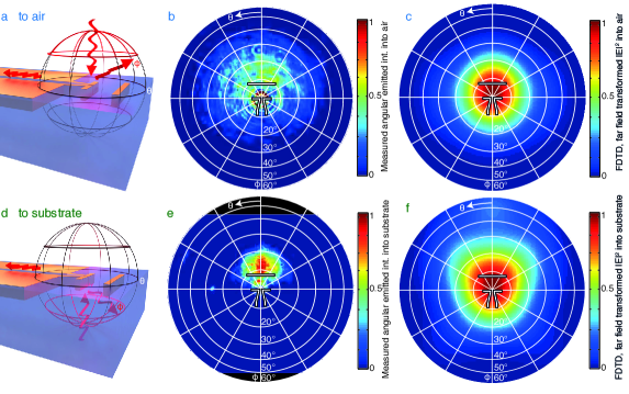
To verify this assumption, the antenna was excited from air (Fig. 3a) and from substrate (Fig. 3d), while the far-field emission of the antenna was imaged into the excitation direction (Figs. 3b,e) in the Fourier plane and compared to the angular emission spectrum obtained from 3D FDTD simulation with the same geometry parameters and excitation (Figs. 3c,f).
In experiment and simulation the antenna emits with strong directionality within a polar angle cone of , which is remarkably narrow17, 23 and completely covered by the NA of our objectives ( from air and immersion from silica). Hence, radiative losses seem to play a minor role in our measurements.
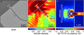
However, the guided field in a waveguide cannot be directly measured in the far-field, with the only limited information coming from slight scattering of impurities in strongly overexposed leakage microscopy (see supplementary). Therefore aperture near-field scanning optical microscopy (NSOM) was used to image the antennas and waveguides (Fig. 4a) directly.
The field distribution of the focused beam at the antenna, as predicted by 3D FDTD simulations (Fig. 4c), leads to a distortion of the incident beam in the area between the antenna feed element and the reflector (Fig. 4b). No propagating waves are visible along the surface of the sample away from the antenna, demonstrating the efficiency of the Yagi reflector. We note that the evanescent field of the guided mode inside the waveguide is still possible to image through the 320 nm thick cladding layer, which is an advantage for probing the operation of the nano-circuit dynamics.
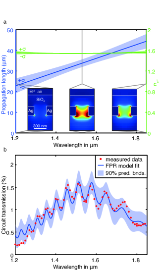
Embedded SPP channel waveguides feature a characteristic propagation length and effective refractive index. In particular the latter property is important for potential applications as it determines the phase velocity, but it is usually difficult to measure, as phase information is lost when measuring emitted intensities. From transmission measurements on circuits with short waveguides, we found spectral oscillations on the total transmission with maximum amplitude at the antenna resonance, which correspond to Fabry-Pérot resonances, allowing us to probe the mode index of the waveguides.
For the shortest waveguides (), the spectral oscillations are very distinct (Fig. 5b). The lumped circuit transmission model (Fig. 2a) allows us to treat the circuit as a Fabry-Pérot resonator defined by a channel waveguide of length and mirrors formed by the antennas, due to imperfect antenna impedance-matching.
This model was fitted to the spectral system transmission, taking the already determined waveguide loss (Fig. 5a, blue curve) and the antenna efficiency into account. Hence, the effective refractive index of the waveguide mode (Fig. 5a, green curve) was determined to be at with low spectral dispersion, a value which coincides well with the expected guided mode effective index from FDTD calculations. Simulated modal field distributions (Fig. 5a, insets) indicate decreasing confinement and increasing field-overlap with the dielectric for longer wavelengths26, thus explaining the experimentally observed decrease in propagation loss for these wavelengths (Fig. 5a, blue curve).
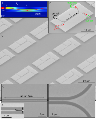
We integrated the developed Yagi antennas and waveguides with optical directional couplers (ODC) in the developed nano-plasmonic circuit platform, demonstrating the functional application of sub-diffraction plasmonics as ultra-short coupling length devices.
ODCs have been a standard component in macroscopic integrated and fiber optics for several decades11. They allow for defined, dispersion-engineered transfer of power from one waveguide (bar) to a second waveguide (cross) by evanescent coupling of the field of the guided modes, which can be well described with coupled-mode-theory10. The coupling-ratio can be tuned with the length of the coupler. In the investigated nano-circuits, two embedded SPP waveguides run in parallel for up to (Fig. 6b).
3D FDTD simulations of the ODC (Fig. 6a) clearly show that with thin metal filaments between the two waveguides the investigated geometry features coupling lengths for a first full power transfer from bar to cross down to few micrometers.
Feed (Fig. 6b, red) and probe antennas (Fig. 6b, green) and an additional fourth antenna for monitoring internal back-reflections (Fig. 6b, blue) are connected to the different ports of the ODC. As before, the emission antennas are all turned by , radiating with a linear polarization perpendicular to the excitation antenna. The length of the couplers was varied in an array of optical circuits (Fig. 6c) from in steps in one direction, while the nominal width of the filament that separates the waveguides was varied from in steps in the other.
Even the smallest, thin metal filaments (aspect ratio for a metal film) demonstrated good fabrication fidelity over the entire length of the longest couplers (Figs. 6d,e). To enable smooth transitions, the cross waveguide approaches the bar waveguide in a bend with a radius of , which for the single waveguide circuits showed negligible bend loss. Fabrication was consistently reproducible with 4 different samples.
As for the basic straight waveguide system, the directional coupler was spectrally probed and modeled with a slightly more elaborate lumped circuit model (Fig. 7a) in which the previously investigated Yagi antennas are connected to the directional coupler with a characteristic spectral transmission and coupling length . Each circuit was probed at , while two clearly distinct emission spots from the cross and bar antenna were separately integrate and the total system transmission was monitored similar as for the single waveguide circuits (Fig. 7e, see supplementary for details).
We note that the resulting power ratio is intrinsically robust to variations of the coupling efficiency into the circuit as those variations simply lead to a linear scaling of the emission from both monitor antennas. Coupled mode theory predicts a power exchange between the waveguides in analogy to two weakly coupled damped harmonic oscillators10. An iterative least-square fit of this model was applied to the measured cross- and bar- emission, while being careful to avoid numerical divergences and ensuring equal weighting of all emission ratios (see supplementary information for details).
Following this fit routine, we obtained a reproducible coupling length of only for the thinnest filament width of . This fit, as a second free parameter, determines an additional equivalent length of the coupler that is caused by the transition into and out of the straight coupling region by bends (Fig. 6).
Hence, even ODCs with a parallel coupler length of demonstrated significant coupling of the guided plasmon from the bar waveguide over to the cross waveguide. Furthermore, direct comparison of experimental and FDTD results demonstrate that the fabricated filament widths are effectively a bit smaller than expected, which is reasonable since the metal side-walls are inclined from the vertical, as is evident from SEM cross-sectional images of the fabricated device (Figs. 1g,h,i).
Consequently, ODCs simulated with a rectangular filament of width (Fig. 6a) had the same coupling length as real couplers consisting of angled filaments. A complete ODC device can therefore be integrated into an unprecedentedly small area11, 27, 28, while maintaining reasonably low loss (Fig. 5a, blue), therefore achieving a single coupling length system transmission of , respectively a loss of .
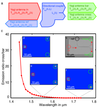
The dispersion of directional couplers is utilized in many compact wavelength division multiplexing (WDM) systems10 as it allows for low-loss wavelength division. Probing the spectral transmission of the investigated ODC circuits reveals a pronounced wavelength-dependence. We characterized different ODCs spectrally in a range of . Starting with , the ODCs with a filament width of and length of (Fig. 7b) operating with several full coupling lengths demonstrated a well-balanced output with (Fig. 7e).
Then, by sweeping the wavelength, we observed full switching between cross (Fig. 7d) and bar (Fig. 7f) in going from short to long wavelengths, leading to a wavelength discrimination between and (see supplementary information for a video demonstrating spectral switching).
The whole device features a footprint of only and could easily be stacked to form an arrayed WDM, enabling even more narrow wavelength discrimination within little more space. The size is extremely compact compared to current dielectric integrated WDMs requiring millimeter dimensions6.
The strong dispersion of the coupling is dominated by the frequency dependent dielectric constant of the Au as the field-penetration into the thin metallic filament between the waveguide is deep.
Thus, inside the ODC the total metal-field overlap is large compared to the single waveguide where the metal-dispersion does not influence the effective index of the mode considerably (Fig. 5a, green curve). However, the low dispersion is a desired property for the waveguides as is the high dispersion of the couplers for reducing the effective size of the ODC.
In conclusion, we have demonstrated a highly reproducible design scheme for plasmonic nano-circuitry that combines the high confinement and dispersive properties of plasmonics28 together with the low loss and high coupling efficiencies of Yagi-Uda antennas. For the first time, loaded optical Yagi antennas are used to reduce insertion loss and couple light with a high total efficiency of ( from air, from substrate) into and out of plasmonic nano-circuits.
Furthermore, this platform is used to demonstrate the operation of embedded SPP based ODCs with extraordinarily short coupling length. The ODCs feature low transmission loss and compete well with other, e.g. Si integrated circuitry components6, 27 in terms of coupling-length-over-loss ratio while being superior in overall compactness.
Distinct spectral switching is observed, thus allowing down-scaling of wavelength division multiplexing from the millimeter to the micrometer range. Additionally, we note that other nano-plasmonic circuitry components can easily be transferred to the Yagi-Uda loaded embedded plasmonic waveguide platform, leading a path towards highly integrated, spectrally functional plasmonic chips like resonant guided wave networks29 or on-chip detectors12, ideally with no need for subsequent intersections5, 7, 8 between different types of waveguides.
The authors thank P. Banzer, T. Bauer, S. Dobmann, J. S. Fakonas and H. W. Lee for inspiring discussions and help with a new optical setup.
This work was supported by the Cluster of Excellence Engineering of Advanced Materials (EAM), Erlangen and the Multidisciplinary University Research Initiative grant (Air Force Office of Scientific Research, FA9550-10-1-0264). A.K. and D.P. also acknowledge funding from the Erlangen Graduate School in Advanced Optical Technologies (SAOT) by the German Research Foundation (DFG) in the framework of the German excellence initiative, A.K. by Friedrich Naumann Foundation and S.P.B. by the National Science Foundation. We acknowledge use of facilities of the Kavli Nanoscience Institute (KNI) at Caltech and the Max Planck Institute for the Science of Light (MPL), Erlangen.
A.K. and S.P.B. conceived the experiments and developed the device design, A.K. performed numerical simulations and S.P.B. fabricated the samples. A.K., D.P., H.P. and S.P.B. performed the optical and FIB/SEM measurements. A.K., S.P.B., U.P. and H.A.A. analyzed the data and wrote the first draft of the manuscript. All authors contributed to the final version of the manuscript.
Experimental details on the fabrication the farfield optical IR setup and characterization procedures, leakage microscopy measurements, spectral switching, NSOM measurements and experimental data analysis and statistics on the antennas and directional couplers and numeric details on the FDTD simulations.
References
- Engheta 2007 Engheta, N. Science 2007, 317, 1698–702
- Miller 2009 Miller, D. A. B. Proc. IEEE 2009, 97, 1166–1185
- Zia et al. 2006 Zia, R.; Schuller, J. A.; Chandran, A.; Brongersma, M. L. Mater. Today 2006, 9, 20–27
- Gramotnev and Bozhevolnyi 2010 Gramotnev, D. K.; Bozhevolnyi, S. I. Nature Phot. 2010, 4, 83–91
- Delacour et al. 2010 Delacour, C.; Blaize, S.; Grosse, P.; Fedeli, J. M.; Bruyant, A.; Salas-Montiel, R.; Lerondel, G.; Chelnokov, A. Nano Lett. 2010, 10, 2922–6
- Asghari and Krishnamoorthy 2011 Asghari, M.; Krishnamoorthy, A. V. Nature Phot. 2011, 5, 268–270
- Gosciniak et al. 2010 Gosciniak, J.; Volkov, V. S.; Bozhevolnyi, S. I.; Markey, L.; Massenot, S.; Dereux, A. Opt. Express 2010, 18, 5314–9
- Briggs et al. 2010 Briggs, R. M.; Grandidier, J.; Burgos, S. P.; Feigenbaum, E.; Atwater, H. A. Nano Lett. 2010, 10, 4851–4857
- Uda 1927 Uda, S. Proc. IRE 1927, 15, 377–385
- Yariv 1973 Yariv, A. IEEE J. Quantum Electron. 1973, 9, 919–933
- Alferness 1986 Alferness, R. C. Science 1986, 234, 825–829
- Ly-Gagnon et al. 2012 Ly-Gagnon, D.-S.; Balram, K. C.; White, J. S.; Wahl, P.; Brongersma, M. L.; Miller, D. A. Nanophotonics 2012, 1
- Cai et al. 2010 Cai, W.; Shin, W.; Fan, S.; Brongersma, M. L. Adv. Mater. 2010, 22, 5120–5124
- Berini and De Leon 2011 Berini, P.; De Leon, I. Nature Phot. 2011, 6, 16–24
- Banzer et al. 2010 Banzer, P.; Peschel, U.; Quabis, S.; Leuchs, G. Opt. Express 2010, 18, 10905–10923
- Novotny and van Hulst 2011 Novotny, L.; van Hulst, N. Nature Phot. 2011, 5, 83–90
- Biagioni et al. 2012 Biagioni, P.; Huang, J.-S.; Hecht, B. Rep. Prog. Phys. 2012, 75, 024402
- Wen et al. 2009 Wen, J.; Romanov, S.; Peschel, U. Opt. Express 2009, 17, 5925
- Wen et al. 2011 Wen, J.; Banzer, P.; Kriesch, A.; Ploss, D.; Schmauss, B.; Peschel, U. Appl. Phys. Lett. 2011, 98, 101109
- Novotny 2007 Novotny, L. Phys. Rev. Lett. 2007, 98
- Andryieuski et al. 2012 Andryieuski, A.; Malureanu, R.; Biagi, G.; Holmgaard, T.; Lavrinenko, A. Opt. Lett. 2012, 37, 1124–1126
- Coenen et al. 2011 Coenen, T.; Vesseur, E. J. R.; Polman, A.; Koenderink, A. F. Nano Lett. 2011, 11, 3779–84
- Curto et al. 2010 Curto, A. G.; Volpe, G.; Taminiau, T. H.; Kreuzer, M. P.; Quidant, R.; van Hulst, N. F. Science 2010, 329, 930–3
- Bernal Arango et al. 2012 Bernal Arango, F.; Kwadrin, A.; Koenderink, A. F. ACS nano 2012, 6, 10156–67
- Dorfmüller et al. 2011 Dorfmüller, J.; Dregely, D.; Esslinger, M.; Khunsin, W.; Vogelgesang, R.; Kern, K.; Giessen, H. Nano Lett. 2011, 11, 2819–24
- Dionne et al. 2006 Dionne, J. A.; Sweatlock, L. A.; Atwater, H. A.; Polman, A. Phys. Rev. B 2006, 73
- Trinh et al. 1995 Trinh, P.; Yegnanarayanan, S.; Jalali, B. Electron. Lett. 1995, 31, 2097–2098
- Boltasseva et al. 2005 Boltasseva, A.; Nikolajsen, T.; Leosson, K.; Kjaer, K.; Larsen, M.; Bozhevolnyi, S. J. Lightwave Technol. 2005, 23, 413–422
- Feigenbaum et al. 2010 Feigenbaum, E.; Burgos, S. P.; Atwater, H. A. Opt. Express 2010, 18, 25584–25595