Broadband ferromagnetic resonance characterization of GaMnAs thin films
Abstract
The precessional magnetization dynamics of GaMnAs thin films are characterized by broadband network analyzer ferromagnetic resonance (FMR) in a coplanar geometry at cryogenic temperatures. The FMR frequencies are characterized as function of in-plane field angle and field amplitude. Using an extended Kittel model of the FMR dispersion the magnetic film parameters such as saturation magnetization and anisotropies are derived. The modification of the FMR behavior and of the magnetic parameters of the thin film upon annealing is analyzed.
I Introduction
Precessional magnetization dynamics of magnetic thin films and nanostructures are highly relevant for magnetic device applications. For example the minimum magnetization reversal times and hence the ultimate data rate of a magnetic memory devices is directly determined by the precession frequency Kaka_APL80_2958_2002 ; Gerrits_Nature418_509_2002 ; Schumacher_PRL90_017201_2003 ; Schumacher_PRL90_017204_2003 . Ferromagnetic semiconductors are a particularly promising class of magnetic materials as they could offer the combination of magnetic memory and semiconductor logic functions in the same material. Presently, GaMnAs can be considered the most prominent prototype of diluted ferromagnetic semiconductors with well determined material parameters Jungwirth_RMP78_809_2006 . The precessional magnetization dynamics of GaMnAs thin films and devices have been characterized by different techniques. Time resolved precessional dynamics have been studied by all-optical pump-probe mageto optics using fs lasers Qi_APL91_112506_2007 ; Rozkotova_APL92_122507_2008 ; Rozkotova_APL93_232505_2008 ; Hashimoto_PRL100_067202_2008 ; Zhu_APL94_142109_2009 or by time resolved magneto-optical characterization upon electrical excitation Hoffmann_PRB80_054417_2009 ; Woltersdorf_PRB87_054422_2013 . Furthermore low-temperature cavity ferromagnetic resonance (FMR) has been used to investigate anisotropies and linewidths Sasaki_JAP91_7484_2002 ; Liu_PRB67_205204_2003 as well as spin wave resonances Goennenwein_APL82_730_2003 . In addition electrical measurements based on photovoltage detection Wirthmann_APL92_232106_2008 or on spin-orbit ferromagnetic resonance Fang_NatureNano6_413_2011 have been tested.
Over the last years broadband vector network analyzer based ferromagnetic resonance (VNA-FMR) Sangita_JAP99_093909_2006 using coplanar wave guides as inductive antennas has become a versatile tool for the simple and fast all electrical characterization of precessional dynamics of various magnetic thin films and multilayers Santiago_JAP110_023906_2011 ; Santiago_JAP109_013907_2011 . In principle low-temperature VNA-FMR Sierra_APL93_172510_2008 should also be suitable for the electrical characterization of ferromagnetic semiconductors such as GaMnAs. However up to now VNA-FMR based measurements of the precessional magnetization dynamics of GaMnAs have proven difficult to achieve. This is due to the low saturation magnetization of GaMnAs in combination with strong crystalline anisotropies. Both properties lead to a rather weak inductive signal which could be easily masked by the noise of the high bandwidth measurement electronics.
Here we present broadband coplanar VNA-FMR measurements of the precessional dynamics of GaMnAs thin films in a cryogenic environment. For sufficiently high excitation powers a clear precessional signal is observed in the VNA-FMR spectra. The field and angular dependence of the FMR peaks can be well described by a Kittel model taking into account the different anisotropy components of GaMnAs. The precessional dynamics and material parameters of an as-grown and an annealed thin film are analyzed and compared.
II Experimental setup and procedure
GaMnAs layers of 100 nm thickness were grown in a low-temperature MBE environment on a 2 inch semi-insulating GaAs(001) wafer at temperatures of = 240°C and 220°C, respectively. Details of the growth and annealing procedure can be found elsewhere BenHamida_JMSJ36_49_2012 . Samples of 10 mm x 10 mm were cut from the wafers as well as 5 mm x 5 mm pieces for superconducting quantum interference device (SQUID) magnetometry. For the as-grown sample of = 240°C a saturation magnetization = 30 mT is measured. The sample with = 220°C was annealed at 200°C for 18 h in ambient air resulting in an increased saturation magnetization of = 74 mT.
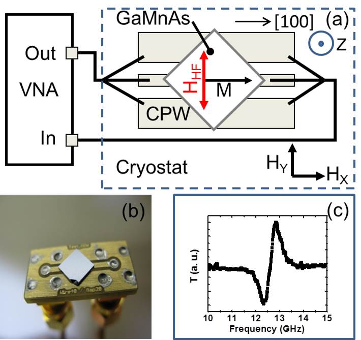
The setup for inductive FMR characterization of the samples is described with respect to Fig. 1. The experiments are carried out in a variable temperature insert of a commercial He cryostat allowing to vary the sample temperature from = 1.5 … 250 K. All FMR measurements of this work were carried out at fixed sample temperature of = 10 K. The cryostat is equipped with a three axial superconducting vector magnet allowing application of static magnetic vector fields = up to 1 T amplitude and arbitrary orientation. For FMR measurements the 5x5 mm2 samples are placed on the center of a coplanar waveguide (CPW). Details of the design and high frequency properties of the CPW can be found elsewhereSievers_IEEETransMag49_58_2013 . Both ends of the CPW are connected to the two ports of a 24 GHz bandwidth VNA via 18 GHz bandwidth coaxial lines of about 1.5 m length. Note that the rather long length of the coaxial lines is determined by the dimensions of the cryostat. Inside the cryostat the CPW substrate is oriented in the -plane with the CPW line running along and high frequency (HF) field generation along ( || ). In the present experiments in-plane magnetic vector fields up to 0.5 T amplitude are applied in the sample plane ( = 0). As sketched in Fig. 1(a) the GaMnAs samples are placed diagonally on the CPW with the [010] crystalline axis oriented parallel to and the [100] axis along .
For an FMR measurement at a given static vector field , the frequency output of the VNA is swept between 1 and 18 GHz and the forward scattering signal is measured. To maximize the weak inductive FMR signal the maximum output power of 20 dBm is applied. The HF output signal generates a HF excitation field around the CPW center conductor line and thus in the GaMnAs thin film sample. Under resonance conditions the GaMnAs magnetization is excited into FMR precession and the signal transmission is reduced leading to a Lorentzian absortion line in the VNA sweep. To enhance the visibility of the FMR signal a VNR reference measurement is carried out at a non-resonant field. The normalized transmission signal T is then deduced by subtracting the reference VNA sweep from the actual measurement data. From the resonance peak the FMR frequency and the absorption line width are derived. Note that for certain applied static fields only weak resonance peaks were found making a reliable linewidth analysis impossible. By variation of the applied static field the FMR properties were measured as function of the field vector .
III Data Analysis
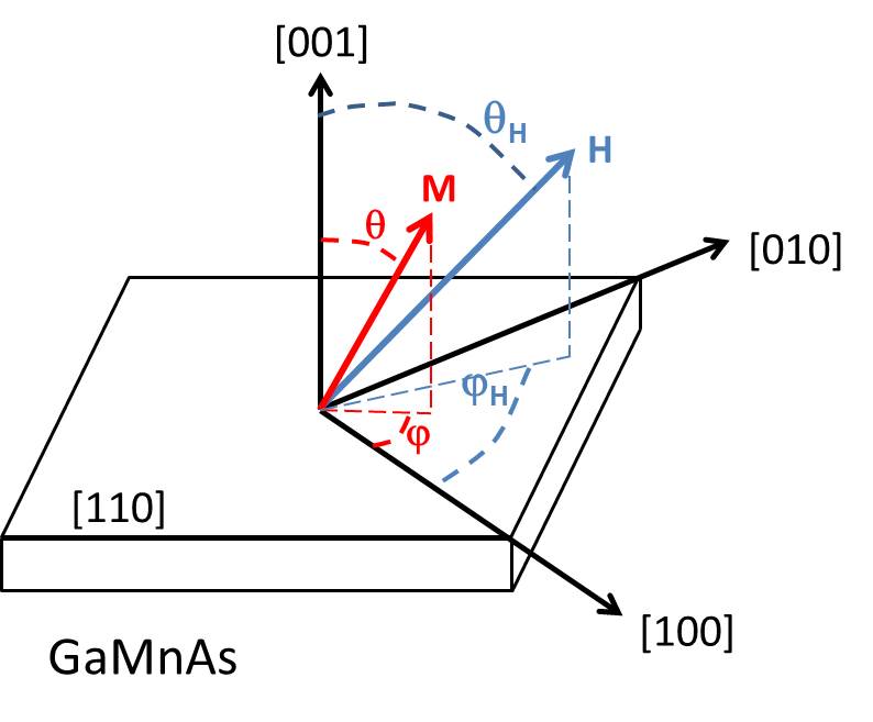
A detailed review on FMR in GaMnAs has been given by Liu and Furdyna Liu_JPCM18_R245_2006 . In an FMR experiment, the magnetization (see Fig. 2 for details of the angle nomenclature) of the film precesses around its equilibrium position with the FMR frequency . Sweeping the value of the applied microwave frequency at a fixed magnetic field (cp. Fig. 2), the resonance condition will be satisfied at . The condition is given by:
| (1) |
where denotes the gyromagnetic ratio and is the free magnetic energy. The expression of for a thin film with crystalline and uniaxial anisotropy is given by:
| (2) | |||||
where (SI units). is the effective magnetization of the thin film. is the in-plane uniaxial anisotropy constant corresponding to the easy axis orientation with respect to the crytallographic direction [100]. is the in-plane cubic anisotropy constant. is the in-plane orientation of the cubic easy axis with respect to [100].
| Sample | ||||||
|---|---|---|---|---|---|---|
| annealed | 74 mT | 30 mT | 70 mT | 45° | 85 mT | 0° |
| as-grwon | 30 mT | 130 mT | -20 mT | 20° | 100 mT | -20° |
During our experiments, the external field is applied in-plane and the film magnetization is assumed to stay also in-plane (°). At a given direction of , the resonance is then obtained by numerically solving the above equation at the equilibrium position of , for . The anisotropy parameters of the GaMnAs thin films can then be derived for example from a fit to the measured angular dependence of the precession frequency at fixed field amplitude H. Fig 3 shows as function of the in-plane field angle for applied field amplitude of = 0.2 T (green) and 0.3 T (red). The symbols represent the measured data whereas the lines are the fits according to the above FMR model. Two sets of data taken on the two different samples are shown. The upper panel (a) shows the data of the annealed sample whereas in (b) the data of the as-grown sample are shown.
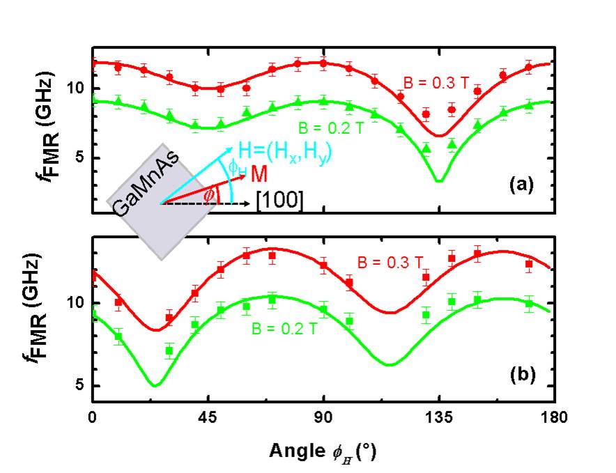
The data of both samples can be well described by a fit to the above model taking into account a thin film with crystalline in-plane cubic and uniaxial anisotropy. The values of the derived anisotropies for the best fit to the data are regrouped in Table 1. Note that in Table 1 the anisotropy fields are given instead of the anisotropy constants .
Note that the values of the saturation magnetization are based on the SQUID measurements and are not derived from fitting. Figure 3 shows that the model based on the above parameters well describe the experimental data both of the annealed and the as-grown sample. The derived values of the magnetic parameters are very reasonable when compared to literature values of thin film anisotropies derived by conventional cavity FMR experiments of GaMnAs thin films Liu_JPCM18_R245_2006 . The comparison of the two parameter sets shows the strong impack of annealing on all magnetic parameters from saturation magnetization to the various anisotropy terms.
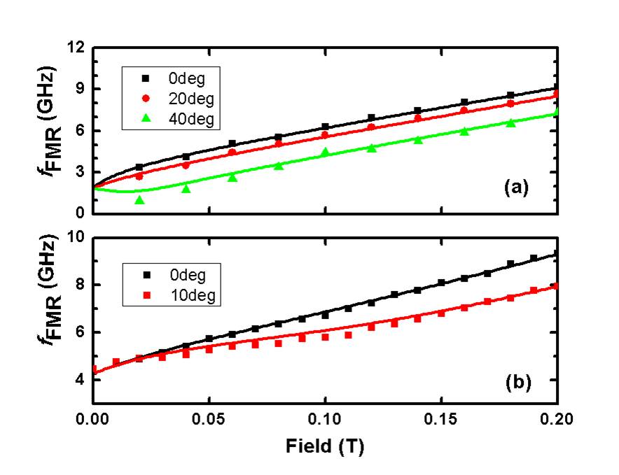
The broadband coplanar FMR setup also allows to derive experimental values of as function of field amplitude for a fixed in-plane angle . Such field dependent data is shown in Fig. 4 for selected field angles for the (a) annealed and (b) as-grown samples. The symbols again represent the data whereas the lines are the model fit. The measured data is again well described by the model fit confirming the feasibility of the derived parameters.
As mentioned above the linewidth could not be systematically analyzed from the VNA-FMR data. However for selected data points a sufficiently clear resonance peak allowed a reliable linewidth analysis. From this linewidth data a Gilbert damping parameter of was derived for the annealed sample. This value is in good agreement with the literature values of annealed samples derived by X-Band ferromagnetic spectroscopy Khazen_PRB77_165204_2008 . It is however worth noting that this value is quite different from literature data derived from time resolved optical pump probe experiments Qi_APL91_112506_2007 for an as-grown sample (the values of ranged from 0.12 to 0.21). The reason of this strong deviation of the literature values of the damping derived by different methods can presently only be subject of speculation. However, it might be related to different applied fields and hence to different contributions of extrinsic line broadening in the experiments Counil_JAP95_5646_2004 . Furthermore the difference could be related to inhomogeneous sample properties Woltersdorf_PRB87_054422_2013 .
IV Conclusion
Concluding we have demonstrated the suitability of broadband network analyze based FMR for the characterization of the precessional dynamics of GaMnAs thin films. A coplanar inductive antenna was used to excite and detect the precessional signal of 100 nm thick annealed and as-grown GaMnAs thin films with saturation magnetization down to 30 mT. The field and angular dependence of the FMR frequency could be well described by a model taking into accound the different thin film anisotropy terms. The simple and yet powerful setup could in the future allow investigations of more complex systems such as of the coupled dynamics of GaMnAs based tunnel junctions and multilayers.
V Acknowledgments
The work was supported by DFG SPP Semiconductor Spintronics and EMRP JRP IND08 MetMags and JRP EXL04 SpinCal. The EMRP is jointly funded by the EMRP participating countries within EURAMET and the EU.
References
- (1) S. Kaka and S. E. Russek. Appl. Phys. Lett., 80:2958, 2002.
- (2) Th. Gerrits, H. A. M. van den Berg, J. Hohlfeld, L. Baer, and Th. Rasing. Nature, 418:509, 2002.
- (3) H. W. Schumacher, C. Chappert, P. Crozat, R. C. Sousa, P. P. Freitas, J. Miltat, J. Fassbender, and B. Hillebrands. Phys. Rev. Lett., 90:017201, 2003.
- (4) H. W. Schumacher, C. Chappert, R. C. Sousa, P. P. Freitas, and J. Miltat. Phys. Rev. Lett., 90:017204, 2003.
- (5) T. Jungwirth, Jairo Sinova, J. Masek, J. Kucera, and A. H. MacDonald. Rev. Mod. Phys., 78:809, 2006.
- (6) J. Qi, Y. Xu, N. H. Tolk, X. Liu, J.K. Furdyna, and I.E. Perakis. Appl. Phys. Lett., 91:112506, 2007.
- (7) E. Rozkotova, P. Nemec, P. Horodyska, D. Sprinzl, F. Trojanek, P. Maly, V. Novak, K. Olejnik, M. Cukr, and T. Jungwirth. Appl. Phys. Lett., 92:122507, 2008.
- (8) E. Rozkotova, P. Nemec, N. Tesarova, P. Maly, V. Novak, K. Olejnik, M. Cukr, and T. Jungwirth. Appl. Phys. Lett., 93:232505, 2008.
- (9) Y. Hashimoto, S. Kobayashi, and H. Munekata. Phys. Rev. Lett., 100:067202, 2008.
- (10) Y. Zhu, X. Zhang, T. Li, L. Chen, J. Lu, and J. Zhao. Appl. Phys. Lett., 94:142109, 2009.
- (11) F. Hoffmann, G. Woltersdorf, W. Wegscheider, A. Einwanger, D. Weiss, and C. H. Back. Phys. Rev. B, 80:054417, 2009.
- (12) G. Woltersdorf, F. Hoffmann, H. G. Bauer, and C. H. Back. Phys. Rev. B, 87:054422, 2013.
- (13) Y. Sasaki, X. Liu, and J. K. Furdyna. J. App. Phys., 91:7484, 2002.
- (14) X. Liu, Y. Sasaki, and J. K. Furdyna. Phys. Rev. B, 67:205204, 2003.
- (15) S. T. B. Goennenwein, T. Graf, T. Wassner, M. S. Brandt, and M. Stutzmann. Appl. Phys. Lett., 82:730, 2003.
- (16) A. Wirthmann, X. Hui, N. Mecking, Y. S. Gui, T. Chakraborty, C. M. Hu, M. Reinwald, C. Schüller, and W. Wegscheider. Appl. Phys. Lett., 92:232106, 2008.
- (17) D. Fang, H. Kurebayashi, J. Wunderlich, K. Vyborny, L. P. Zarbo, R. P. Campion, A. Casiraghi, B. L. Gallagher, T. Jungwirth, and A. J. Ferguson. NatureNano, 6:413, 2011.
- (18) S. S. Kalarickal, P. Krivosik, M. Wu, C. E. Patton, M. L. Schneider, P. Kabos, T. J. Silva, and John P. Nibarger. J. App. Phys., 99:093909, 2006.
- (19) S. Serrano-Guisan, W. Skowronski, J. Wrona, N. Liebing, M. Czapkiewicz, T. Stobiecki, G. Reiss, and H. W. Schumacher. J. App. Phys., 110:023906, 2011.
- (20) S. Serrano-Guisan, Han-Chun Wu, C. Boothman, M. Abid, B. S. Chun, I. V. Shvets, and H. W. Schumacher. J. App. Phys., 109:013907, 2011.
- (21) J. F. Sierra, V. V. Pryadun, F. G. Aliev, S. E. Russek, M. Garcia-Hernandez, E. Snoeck, and V. V. Metlushko. Appl. Phys. Lett., 93:172510, 2008.
- (22) A. Ben-Hamida, N. Liebing, S.Serrano-Guisan, S. Sievers, K. Pierz, and H. W. Schumacher. Journal of the Magnetics Society of Japan, 36:49, 2012.
- (23) S. Sievers, N. Liebing, P. Nass, S. Serrano-Guisan, M. Pasquale, and H. W. Schumacher. IEEE Trans. Magn., 49:58, 2013.
- (24) X. Liu and J. K. Furdyna. J. Phys.: Condens. Matter, 18:R245, 2006.
- (25) K. Khazen, H. J. von Bardeleben, J. L. Cantin, L. Thevenard, L. Largeau, O. Mauguin, and A. Lemaitre. Phys. Rev. B, 77:165204, 2008.
- (26) G. Counil, J.-V. Kim, T. Devolder, C. Chappert, K. Shigeto, and Y. Otani. J. App. Phys., 95:5646, 2004.