Dielectric Environment Effect on Carrier Mobility of Graphene Double-Layer Structure
Abstract
We have theoretically studied the dielectric environment effect on the charged-impurity-limited carrier mobility of graphene double-layer structure (GDLS) on the basis of the Boltzmann transport theory. In this system, two graphene layers are separated by a dielectric barrier layer. It is pointed out that the carrier mobility strongly depends on the dielectric constant of the barrier layer when the interlayer distance becomes larger than the inverse of the Fermi wave vector. Moreover, the conditions to improve the charged-impurity-limited carrier mobility of the GDLS are evaluated.
Recent progress in graphene research has stimulated the fabrication of new functional electronic devices which are composed of graphene and atomically-thin materials. One such superlattice system is a graphene double-layer structure (GDLS), in which two graphene layers are separated by a thin dielectric, as shown in Fig. 1(a). Theoretically the GDLS is considered to be a good platform for studying the exciton superfluidity Pikalov2012 ; Mink2012 , the Coulomb drag effect Mink2012 ; Scharf2012 and plasmon mode Profumo2012 ; Badalyan2012 ; Stauber2012 . Recently, an optical device using this system was also proposed as an application Novoselov2012 . In experiments, Al2O3Kim2011b or -BN Dean2010 ; Ponomarenko2011 ; Lee2012 ; Zomer2012 ; Gorbachev2012 is used as the inner barrier layer. A recent experiment demonstrated that two graphene layers can be electrically separated by inserting a few atomic layers of -BN, which correspond to the interlayer distance nm Gorbachev2012 .
Carrier mobility is one of the key benchmarks of device performance because it determines the power dissipation and switching speed. Recent theory suggests improving carrier mobility by placing a high- overlayer on the semiconductor nanostructure, which leads to weakening of Coulomb scattering due to the screening effect Jena2007 ; Adam2007 . Indeed, several electronic transport measurements on graphene or atomically-thin material have successfully revealed mobility enhancement though change in the dielectric environment Jang2008a ; Kim2009 ; Radisavljevic2011 ; Hollander2011 . However, a systematic study of the dielectric environment effect on the carrier mobility of the GDLS has not been performed yet.
In this letter, we evaluate the dielectric environment effect on the charged-impurity-limited carrier mobility of the GDLS on the basis of the Boltzmann transport theory. We consider the static screening of Coulomb interaction within random phase approximation (RPA). It is found that carrier mobility strongly depends on the dielectric constant of the barrier layer if the interlayer distance becomes larger than the inverse of the Fermi wave vector. Our results offer effective use of ultra-thin dielectric barriers and a practical design strategy to improve the charged-impurity-limited mobility of the GDLS.
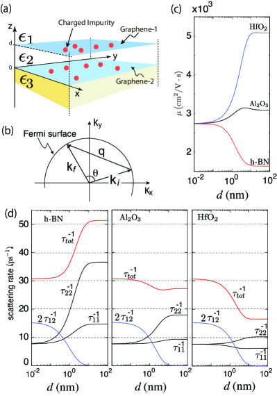
Figure 1(a) shows a schematic of the GDLS, in which two graphene layers are separated by three different dielectrics and . We assume that the two graphene layers are coupled only through Coulomb interaction between the charged impurities and carriers. The wavefunction of the carrier in a graphene layer is described as the function in the -direction Ando2006 . The Hamiltonian can be written as
| (1) | ||||
where () is the creation (annihilation) operator for an electron with wavevector (,) and pseudospin on the -th graphene layer. Here eVÅ is the band parameter. and are the Pauli spin matrices for pseudospin; are pseudospin labels to describe the sublattice of the honeycomb lattice. is the area of each graphene layer. denotes the Fourier component of the screened Coulomb potential, which depends on the interlayer distance , and includes the effect of Coulomb interaction between carriers on each graphene layer through the polarization function Ando2006 . is the particle density of random impurities on the -th graphene layer having total number of impurities . represents the position of the impurities on the -th layer.
The carrier mobility can be described by using the carrier concentration and conductivity ; Nomura2006 ; Ando2006a . Here we assume that the imbalance of carrier concentration between two graphene layers is absent. The total scattering rate at Fermi energy is given as . Here () is the intralayer scattering rate of the first (second) graphene layer, and and are interlayer scattering rates. According to the semiclassical Boltzmann theory, the momentum scattering rate is given by
| (2) |
where is the impurity concentration on first (second) graphene layer. The impurity concentration for interlayer scattering is given as the average of two layers . For simplicity, we assume that the impurity concentration at each layer are equivalent and that the Fermi level of both graphene layers lies in the conduction band. is the density of states of single layer graphene with owing to the valley and spin degeneracy. is the scattering angle, and is the scattering wave vector on the circular two-dimensional Fermi surface as shown in Fig. 1(b). The Fermi wave number on each graphene layer is given as . In the present assumption, since the carrier concentration for each layer is identical, the interlayer scattering rate is equivalent, i.e. . Note that the last dependent factor also contains the phase of the wave function of grapheneAndo2006 ; Nomura2006 . Structural parameter such as the interlayer distance and scattering potential due to charged impurities are included in the screened potentials .
Here we briefly explain the derivation of the screened Coulomb potential from the unscreened one . The analytical expression of the unscreened Coulomb potentials of the GDLS can be derived with the image charge method Kumagai1989 ; Jena2007 . For this system, we need to consider an infinite series of point image charges arising from two interfaces at and shown in Fig.1(a), where two types of dielectrics are spanned by a graphene layer. The resulting unscreened Coulomb potentials are given as
| (3) | ||||
| (4) | ||||
| (5) |
Here and are the intralayer Coulomb interactions on the first and second graphene layer, respectively. is the interlayer Coulomb interaction. These potentials have been used in the context of the superfluid magnetoexitons Pikalov2012 and plasmon mode Badalyan2012 ; Profumo2012 of the GDLS. The above expressions indicate that the parameter () determines the screening behavior and the strength of interlayer Coulomb interaction. For , the interlayer interaction becomes negligible ; that is, the two graphene layers are independent. In contrast, for , the two graphene layers are rather strongly bounded through the interlayer Coulomb interaction. The screened Coulomb potentials are given by the following RPA equation,
| (6) |
where . is the static polarization function of single layer graphene Ando2006a ; Hwang2007 . By combining Eqs. (2)-(6), we can evaluate the carrier mobility and scattering rate of the GDLS.
We first investigate the dependence of the mobility on the interlayer distance. To focus on the role of , we consider three different dielectrics as the middle layer, that is, -BN, and . Those dielectric constants are , and , respectively Gorbachev2012 ; Frederisk1991 ; Desgreniers1991 ; Kang2000 . Other ultrathin dielectrics with high- can be candidates for the inner barrier layer in further studiesWilk2001 ; Osada2012 . Here we assume that the top and bottom dielectrics are air and , respectively: and .
Figure 1(c) shows the dependence of mobility on the interlayer distance for three different middle dielectrics . The mobilities are independent of at a smaller interlayer distance ( nm). With increasing interlayer distance, the effect of the middle layer dielectric becomes prominent. In the large ( nm) limit, that is, , the carrier mobilities strongly depend on , because the interlayer Coulomb interaction becomes negligible. Thus the carrier mobility can be improved by inserting the higher dielectrics as the middle layer.
The strong dependence for the thicker region can be attributed to the decay of interlayer scattering. Figure 1(d) shows the -dependence of three components of the scattering rate (,) and the total scattering rate () for three different dielectrics. The intralayer components, and , strongly depend on , whereas the interlayer component is almost independent of and decays for wider regions.
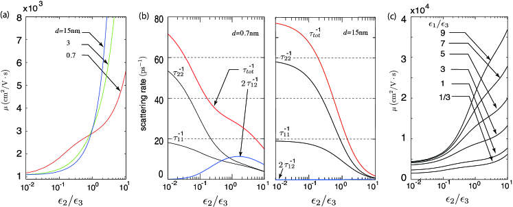
Figure 2(a) shows the dependence of the carrier mobility on for several fixed interlayer distances. We can see that the carrier mobility monotonically increases with the ratio when the interlayer distance becomes wider; see the case of and nm. However, for the thinner case nm, i.e., the mobility increases more quickly when , however its growth rate slows at . Thus, the combination of dielectrics with should be chosen to improve the mobility for the thinner GDLS.
The nonmonotonic behavior for the nm case can be related to the development of the interlayer scattering rate . Figure 2(b) shows the total scattering rate together with its components , and as the function of the middle layer dielectric constant for (left panel) and nm (right panel). Here we can see that the interlayer component grows in the higher region for the case nm owing to the stronger interlayer interaction. For this reason, the mobility at nm in the lower region is improved. In higher region, however, the mobility at nm becomes lower than the mobility at and nm owing to growth of the interlayer component . This interlayer screening effect is effective at and is negligible at . The enhancement of interlayer screening effect for the region of indicates that the carrier transport properties are strongly affected by the interlayer interaction due to the charged impurities. Since such scattering mechanism has not been considered in conventional theory of Coulomb drag, it might be necessary to include the interlayer screening effect for GDLS with small , which is available in recent experiment Gorbachev2012 .
So far, we have fixed the dielectric constants for the top and bottom layers at and , respectively. Next we focus on the effect of the dielectric environment from top or bottom layers on the carrier mobility at nm, which satisfies the criteria of , that is, the interlayer screening is not negligible. Figure 2(c) shows the carrier mobility as a function of for several ratios of the dielectric constants on the top and bottom layer. This figure clearly shows that the mobility gradually improve with increasing and that the interlayer screening effect also works in higher region of . Therefore, the region of which the mobility at nm is higher than that at and nm, widens with increasing .
In conclusion, we have investigated the dielectric environment effect on the charged-impurity-limited carrier mobility of the GDLS on the basis of the Boltzmann transport theory. The carrier mobility of GDLS strongly depends on the interlayer distance, and can be elevated drastically by using high materials as the middle layer. Our result shows that the mobility can be improved by inserting higher dielectric materials into thicker GDLS. For thinner GDLS, however, the mobility can be improved by choosing a combination of dielectrics with . This condition originates from the interlayer screening effect due to strong interlayer coupling. Our results are intended as guidelines for experiments and applications of new functional atomically-thin devices.
This work is supported by a Grant-in-Aid for Scientific Research (KAKENHI) (Nos. 24710153 and 23310083) from the Japan Society for the Promotion of Science.
References
- (1) A. A. Pikalov and D. V. Fil, Nanoscale Res. Lett. 7, 145 (2012).
- (2) M. P. Mink, H. T. C. Stoof, R. A. Duine, M. Polini, G. Vignale. Phis. Rev. Lett. 108, 186402 (2012)
- (3) B. Scharf and A. Matos-Abiague, Phys. Rev. B86, 115425 (2012)
- (4) T. Stauber and G. Gomez-Santos, Phys. Rev. B85, 075410 (2012).
- (5) S. M. Badalyan and F. M. Peeters, Phys. Rev. B85,195444 (2012).
- (6) R. E. V. Profumo, R. Asgari, M. Polini, and A. H. MacDonald, Phys. Rev. B85, 085443 (2012).
- (7) K. S. Novoselov and A. H. Castro Neto, Phys. Scr. T146 014006(2012).
- (8) S. Kim, I. Jo, J. Nah, Z. Yao, S. K. Banerjee and E. Tutuc, Phys. Rev. B83, 161401 (2011).
- (9) C. R. Dean, A. F. Young, I. Meric, C. Lee, L. Wang, S. Sorgenfre, K. Watanabe, T. Taniguchi, P. Kim, K. L. Shepard and J. Hone, Nat. Nanotechnol. 5, 722 (2010)
- (10) L. A. Ponomarenko, A. K. Geim, A. A. Zhukov, R. Jalil, S. V. Morozov, K. S. Novoselov, I. V. Grigorieva, E. H. Hill, V. V. Cheianov, V. I. Fal’ko, K. Watanabe, T. Taniguchi, R. V. Gorbachev, Nat. Phys. 7, 958 (2011).
- (11) G. H. Lee, Y. J. Yu, C. Lee, C. Dean, K. L. Shepard, P. Kim, and J. Hone, Appl. Phys. Lett. 99, 243114 (2011).
- (12) P. J. Zomer, S. P. Dash, N. Tombros and B. J. van Wees, Appl. Phys. Lett. 99, 232104 (2011).
- (13) R. V. Gorbachev, A. K. Geim, M. I. Katsnelson, K. S. Novoselov, T. Tudorovskiy, I. V. Grigorieva, A. H. Macdonald, S. V. Morozov, K. Watanabe, T. Taniguchi, L. A. Ponomarenko, Nat. Phys. 8, 896 (2012).
- (14) D. Jena and A. Konar, Phys. Rev. Lett. 98, 136805 (2007).
- (15) S. Adam, E. H. Hwang, V. M. Glitski, and. S. Das Sarma, Proc, Natl. Acad. Sci. U.S.A 104, 1392 (2007)
- (16) C. Jang, S. Adam, J.-H. Chen, E. D Williams, S. Das Sarma, and M. S. Fuhrer, Phys. Rev. Lett. 101, 146805 (2008).
- (17) S. Kim, J. Nah, I. Jo, D. Shahrjerdi, L. Colombo, Z. Yao, E. Tutuc and S. K. Banerjee, Appl. Phys. Lett. 94, 062107 (2009).
- (18) B. Radisavljevic, M. B. Whitwick, and A. Kis, Nat. Nanotechnol. 6, 147 (2011).
- (19) M. J. Hollander, M. Labella, Z. R. Hughes, M. Zhu, K. A. Trumbull, R. Cavalero, D. W. Snyder, X. Wang, E. Hwang, S. Datta and J. A. Robinson, Nano Lett. 11, 3601 (2011).
- (20) T. Ando, J. Phys. Soc. Jpn 75, 054701 (2006).
- (21) K. Nomura and A. H. MacDonald, Phys. Rev. Lett. 96, 256602 (2006).
- (22) T. Ando, J. Phys. Soc. Jpn. 75, 074716 (2006).
- (23) M. Kumagai and T. Takagahara, Phys. Rev. B40,12359 (1989).
- (24) E. H. Hwang and S. Das Sarma, Phys. Rev. B75, 205418 (2007).
- (25) B. G. Frederisk, G. Apai, and T. N. Rhodin, Phys. Rev. B44, 1880 (1991).
- (26) S. Desgreniers and K. Lagarec, Phys. Rev. B59, 8467 (1999).
- (27) L. Kang, B. H. Lee, W.-J. Qi, Y. Jeon, R. Nieh, S. Gopalan, and J. C. Lee, IEEE Electron Device Lett. 21, 181 (2000).
- (28) G. D. Wilk, R. M. Wallace, and J. M. Anthony, J. Appl. Phys. 89, 5243 (2001).
- (29) M. Osada and T. Sasaki, Adv. Mater. 24, 210 (2012).