Transient stimulated emission from multi-split-gated graphene structure
Abstract
Mechanism of transient population inversion in graphene with multi-splitted (interdigitated) top-gate and grounded back gate is suggested and examined for the mid-infrared (mid-IR) spectral region. Efficient stimulated emission after fast lateral spreading of carriers due to drift-diffusion processes is found for the case of a slow electron-hole recombination in the passive region. We show that with the large gate-to-graphene distance the drift process always precedes the diffusion process, due to the ineffective screening of the inplane electric field by the gates. Conditions for lasing with a gain above 100 cm-1 are found for cases of single- and multi-layer graphene placed in the waveguide formed by the top and back gates. Both the waveguide losses and temperature effects are analyzed.
pacs:
72.80.Vp, 73.63.-b, 78.45.+hI Introduction
Conventional scheme of semiconductor laser Koechner-Silfvast is based on population inversion between electron states in conduction and valence bands, so that the emission wavelength is determined by the bandgap of the material used (typically, lasing takes place in a spectral region from near-IR to far-UV). Lasers for mid-IR and THz regions were realized based on the tunnel-coupled heterostructures (quantum cascade schemeGmachl-RPP-2001 ) or on the -type bulk materials with the degenerate valence bands Komiyama-AP-1982 . Active studies of graphene, which is a two-dimensional gapless semiconductor with unusual physical characteristicsCastroNeto-RMP-2009 , involve both theoretical investigation of the stimulated emission regime under steady-state or ultrafast pumping Ryzhii-JAP-2007 ; Vasko-PRB-2010 and experimental attempts - approaches for realization of lasing. Recently, the transformation of the ultrafast optical pumping into THz or near-IR radiation was reported, see Refs. Boubanga-PRB-2012, ; Prechtel-NC-2012, ; Li-PRL-2012, . Due to the emission of optical phonons after the ultrafast pumping Boubanga-PRB-2012 , these approaches should lose an efficiency with increasing pulse duration. In order to avoid the suppression of stimulated emission, one needs a pumping scheme which permits to create dense electron-hole plasma without involvement of the high-energy states when the optical-phonon emission becomes essential. Thus, investigation of alternative pumping mechanisms for realization of population inversion in electron-hole plasma of graphene is timely now.
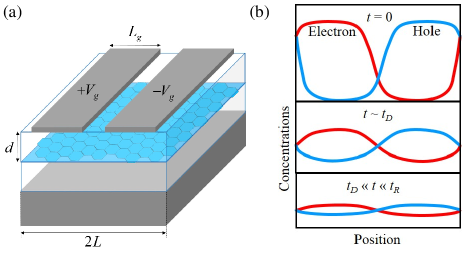
In this paper, we suggest a new pumping scheme for a graphene layer modulated by spatio-temporally varied voltages applied through multi-splitted gates (MSG), see the structure in Fig. 1(a). An initial periodical modulation of electron and hole concentrations shown in Fig. 1(b) takes place at under bipolar voltages applied through the top gates of the MSG structure. Temporal evolution of the initial charge distributions due to lateral spreading of carriers after abrupt switch-off voltages at is shown in the middle panel of Fig. 1(b). If recombination processes are negligible, in-plane spreading of electrons and holes drifted by the electric field created by themselves takes place with a time scale , followed by their diffusion within time , where is the characteristic time for non-radiative recombination, without changing the total electron and hole concentrations which are determined by the initial conditions at . The MSG structure also works as a waveguide where the multi-splitted top and back gates define the vertical confinement and waves propagate along the waveguide.
Under a typical disorder level, the drift-diffusive hydrodynamic equations describe regime of spreading at , when the initial distributions transform into homogeneous quasi-Fermi distributions of electrons and holes. If transient stimulated emission due to direct interband transition in the spectral region takes place during time scales less or comparable to the characteristic time in the passive region (at energies less than a half of the optical-phonon energy), an effective regime for the transient stimulated emission is accomplished.
The paper is organized as follows. In the next section we calculate the distributions of carriers in the biased structure under consideration. In Sec. III, we analyze the process of lateral drift and diffusion of carriers after the bias voltages are abruptly switched-off. The transient lasing regime is considered in Sec. IV. The last section includes the list of approximations used and conclusions. In Appendix we evaluate the hydrodynamic equations describing a temporal evolution of non-uniform electron-hole plasma.
II Initial electron and hole distributions
We start from consideration of the initial distribution of electron and hole concentrations under the biases applied through the multi-splitted top gates separated by the distance from graphene placed at over the substrate with the grounded bottom gate at . The two-dimensional Poisson equation
| (1) |
should be supplied by periodic boundary conditions along the structure (-direction, here is the length of the two-strip element with and voltages), boundary conditions at the top gates and bottom gate, and , and boundary conditions far from the structure, . Boundary conditions at the graphene layer are given by the continuity requirement and the Gauss theorem:
| (2) |
Here is the static dielectric constant, which is the same for the layers under and above the graphene layer, and is the total charge density in the graphene layer, where and are the electron and hole charge densities, respectively.
Initial distributions of the potential and the charge densities can be found by solving Eq. (1) self-consistently with the following relation between the charge densities and the potential in the graphene layer, :
| (3) |
where and , is the carrier temperature, and is the quasi-Fermi distribution with the carrier velocity cm/s.
The charge densities and potential would be obtained from Eqs. (1) and (3) analytically as and , in case when the parallel-plate model could be applicable, the temperature would be zero, and the quantum capacitance of graphene could be ignored. However, the parallel-plate model is not applicable in our case, due to the limitation of the vertical dimension that determines the operating frequency of the waveguide structure and the magnitude of gate voltages in order to have population inversion up to that frequency. Intending waveguide structures operating at mid-IR wavelengths, in the discussion below we shall set the structural parameters as m, m, m, and (SiO2), and with thickness of the gates fixed to nm. However, it should be mentioned that SiO2 has sharp absorption peaks at and m Kitamura-AO-2007 . Therefore, we shall focus on , , and m (corresponding to , , and THz, respectively). In general, either adapting non-polar waveguide materials or avoiding absorption peaks in polar materials is preferable to avoid the dielectric loss in the THz/mid-IR region.
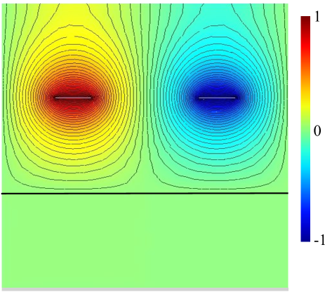

Figure 2 shows the normalized potential distribution, , with m, m, and m at K and V, and Fig. 3 shows electron and hole concentrations, with different gate voltages. As expected, the gate voltages induce electrons and holes in the graphene layer, in which the potential is slightly fluctuated from zero to have nonzero charge densities. Since we have the gates placed far away from the graphene layer, the electron and hole charge densities are smaller than those obtained using the parallel-plate model, , and they have sinusoidal-like shapes. Moreover, since we have the ratio of close to unity, the electric field in the graphene layer created by one gate is canceled due to the fringe effect by the other gate with opposite-signed voltage, so that the charge densities are further reduced. The electric field is mostly concentrated at the edges of the gates, reflecting their thickness much smaller than their length. The maximum field for the highest voltage is close to but still below the breakdown field of SiO2, MV/cm. Sze On the other hand, the field is almost zero in between the graphene layer and the bottom gate due to the screening.
III Transient Lateral Drift-Diffusion and Population Inversion
After the abrupt switch-off of the gate voltages, the carriers spread over the graphene layer by the lateral drift-diffusion processes. In the limit of effective intercarrier scattering and momentum relaxation due to the elastic scattering on structural disorders, these processes are governed by the hydrodynamic equations described in Appendix, Eqs. (17) and (18), coupled with the self-consistent Poisson equation, Eq. (1). In this section, they were solved numerically as nonlinear equations for the quasi-Fermi levels for electrons and holes, , using the standard finite-difference scheme. As mentioned above, we also assume that recombination processes are suppressed.

Figures 4(a), (b), and (c) show the time and position dependences of the electric field, electron concentration, and electron quasi-Fermi level, respectively (see also Fig. 5). Here the same parameters as in Fig. 2 were used and, we have an additional parameter, , which characterizes the total scattering rate caused by structural disorders (see Appendix for details). Hole concentration and its quasi-Fermi level are just equal to mirror images of Figs. 4(b) and (c). They show two distinct time scales of relaxation of these quantities towards their steady states. One is about ps, and it is associated with a process that continues until the electric field created by carriers becomes negligibly small, thus identified as the drift process. The other is about ps and is due to the diffusion process. In our case where is comparable to and therefore the screening of the inplane electric field by the gates is ineffective, the time scale of the drift process is always much faster than that of the diffusion process, unless the quasi-Fermi level is not too large. It can also be seen from Fig. 4(c) that more or less uniform distribution of the electron quasi-Fermi level around meV is reached and population inversion in the THz range through the entire graphene layer is established just after the drift process. Qualitatively speaking, this is shorter than the time scale of nonradiative recombination via optical phonons, which is in between ps (see, for example, Ref. Satou-JAP-2013, ).
Figure 5 shows the time dependence of the electron quasi-Fermi level at the center of the graphene layer with different values of . The time scales increase simultaneously when increases, since the carrier spreading becomes slower when its scattering becomes more frequent. A dimensional analysis shows that the time scales are proportional to . Moreover, they are almost proportional to when , , and are scaled linearly to . On the other hand, when fixing and while scaling and , the time scale of the drift process is roughly proportional to whereas that of the diffusion process remains proportional to .
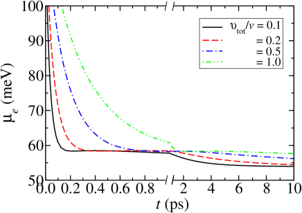
Figure 6 shows the minimum electron quasi-Fermi level at ps as a function of gate voltage with different half-period lengths and different gate lengths , together with . As can be seen in Figs. 4(c) and 5, we have more or less uniform quasi-Fermi level at the time ps for , so that it makes sense to discuss about a single quasi-Fermi level (we took the minimum quasi-Fermi level to ensure that population inversion at a certain energy takes place all over the graphene layer). It is clear from Fig. 6 that the quasi-Fermi level increases monotonically as the voltage increases. Also, it increases as the gate length increases. The condition of population inversion, , for m is fulfilled at voltage V depending on the gate length and the half-period length . Since we have neglected the nonradiative recombination, the quasi-Fermi level is solely determined by the initial concentration and, thus, by the electrostatics through the gate voltages and geometrical parameters in a non-trivial way. In particular, threshold voltages for the same value of the quasi-Fermi level are lower for m than those for m. This lowering is associated with the larger ratio of in the former case, where the cancellation of the electric field in the graphene layer discussed in the previous section is largely relaxed and thereby the induced charge densities as well as the total charges become larger.

From the aspect of the breakdown field, detailed numerical analysis showed that the maximum field at the gate edges to obtain the same value of quasi-Fermi level (say, meV) varies a little by the value of for a fixed value of , although there exists an optimal value of ; for example, for m, the maximum field ranges from to MV/cm when m, having the minimum value at m. In conjunction with the fringing effect mentioned above, the maximum field becomes several times smaller as changes from to m (reduced to around MV/cm). Note that for too long , the time scale of the drift process becomes longer, so that the nonradiative recombination effectively takes place before the drift process completes, and the condition of population inversion might not be fulfilled. It is worth mentioning that the results obtained in this section depend only weakly on the temperature through the temperature dependence of the quasi-Fermi level for fixed charge densities. In particular, the quasi-Fermi level becomes slightly larger as the temperature becomes lower. However, this is not the case for gain of the waveguide since values of distribution functions around the quasi-Fermi level mainly determine the gain and depend much on the temperature.
IV Transient Gain of MSG Structures
Finally, we turn to estimate gain in the MSG structure. We determine the electric field of TE mode propagating along the waveguide from the wave equation
| (4) |
Here we take into account the dielectric loss by introducing the complex dielectric constant, , while we assume . We use the boundary conditions at multi-splitted and bottom gates . We set to the boundary condition at the multi-splitted gates because the gate period is shorter than the wavelength.
At the graphene layer we use a continuity requirement and a boundary condition
| (5) |
which is written through the high-frequency conductivity of graphene, . Using the solution of Eqs. (4) and (5), with , one obtains the dispersion relation between the wavenumber and the frequency :
| (6) |
Since the Drude-like conductivity is negligibly small at the designed frequencies of the waveguide, the conductivity can be written as
| (7) |
where and is the quasi-Fermi distributions of electrons and holes with temperature and quasi-Fermi levels . Here we take the minima of the quasi-Fermi levels to avoid the complication by their position dependence in the transient behavior discussed in the previous section. In case of multi-layer graphene, the conductivity roughly becomes -fold larger, where is the number of graphene layers.
Taking into account the smallness of , we derive the explicit expression of the complex wavenumber from Eq. (6):
| (8) |
Away from the condition , the following approximate expressions for the gain defined as and the real wavenumber can be obtained from Eq. (8):
| (9) |
for . This case corresponds to a propagating mode with relatively small gain. In the opposite case, we have a quasi-standing-wave mode with high gain, which is not of our interest. Considering the nonnegligible absorption by SiO2, it turns out that the waveguide under consideration has a rather narrow bandwidth for the propagating mode around the central frequency when the thickness is fixed. Writing the imaginary part of the dielectric constant through the absorption index (), the condition of positive gain can be readily obtained from Eq. (9) for multi-layer graphene:
| (10) |
where is the fine structure constant. Since the left-hand side in Eq. (10) is smaller than , we have a rather universal expression for the maximum allowed value of the dielectric loss for positive gain, .
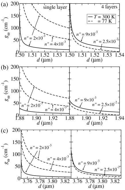
Figure 7 shows the dependence of gain on the thickness with operating wavelengths , , and m, quasi-Fermi levels , , and meV, respectively, different absorption indices, different temperatures, and different numbers of graphene layers, using Eq. (8). Note that for each wavelength under consideration the condition of population inversion is satisfied with corresponding quasi-Fermi level. We plotted Fig. (7) for the thickness larger than (, , and m for , , and m, respectively), which correspond to the propagating mode. At the condition the values of the gain and real wavenumber coincide. It is seen from Fig. (7) that the gain above cm-2 is achieved and that the gain decreases as the thickness increases; the real wavenumber increases as understood from Eq. (9). Thus, one needs to choose carefully a proper value of the thickness (slightly larger than ) to have sufficiently large real wavenumber while keeping the gain larger than losses. Conversely, once the thickness is determined, the operating wavelength is limited in a rather narrow-band range.
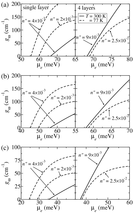
Figure 8 shows the dependence of gain on the quasi-Fermi level with a fixed thickness for each operating wavelength. The real wavenumber does not noticeably change by the quasi-Fermi level. It is seen in Fig. 8 that the gain increases almost linearly to the quasi-Fermi level, starting from the onset of positive gain described by Eq. (10), and it saturates after the increase in the quasi-Fermi level by temperature. Owning to the factor in the expression of , the gain increases as the operating wavelength decreases.
Figures 7 and 8 exhibits a relatively strong temperature-dependence of the gain. This reflects the fact that the interband negative conductivity is linearly dependent on values of distribution functions as seen in Eq. (7), resulting in the increase in its absolute value for the frequency below the quasi-Fermi level as the temperature decreases. Thus, at low temperature the positive gain appears for the higher absorption index. It in turn means that for a fixed absorption index the threshold quasi-Fermi level for the positive gain becomes lower at lower temperature, although above the threshold the positive gain quickly saturates and the magnitude remains more or less the same below K. Also, the introduction of multi-layer graphene greatly enhances the gain. The absorption index experimentally measured for fused silica glasses in Ref. Kitamura-AO-2007, is above , although a smaller value is expected by a thermally grown crystalline SiO2 on a Si substrate. As seen in right panels of Fig. 7, the dielectric loss in such a case can be overcome by introducing multi-layer graphene and by operating at low temperature. One can alternatively use nonpolar materials with no large absorption in the mid-IR wavelength as a part of the MSG structure, e.g., in the substrate region, where materials with relatively low breakdown field are permissible.
V Conclusions
With the main goal to find conditions for an effective stimulated emission regime without the optical-phonon emission, we have examined a new pumping scheme for a graphene layer modulated by spatio-temporally varied voltages which are applied through the multi-splitted top gates. We found that a transient lasing regime in the mid-IR spectral region is realized in the MSG structure with micrometer width and period. Gain above hundred(s) cm-1 for operating wavelengths , , and m was obtained if the gate voltage is around 100-300 V. This is comparable to gain in typical quantum cascade lasers Jovanovic-APL-2004 and the transient stimulated emission takes place if waveguide losses are comparable to losses in quantum cascade lasers.
Let us discuss the assumptions we used in the presented calculations. Because a luck of data on graphene structures with multi-splitted gates, the above consideration was separated into description of the different stages of evolution (i.e., diffusion from the separated electron and hole distributions at initial moment to the homogeneous electron-hole plasma) and estimates of the gain at a time when the recombination is negligible (see numerical data for recombination rate in Ref. Rana-PRB-2009, ). We considered the simplified periodical geometry (the edge effects require a special consideration) placed into a media with homogeneous dielectric constant. A more complicate spatio-temporal simulation does not change the numerical estimates presented here and it should be performed for a specific structure. In calculating the waveguide mode of the MSG structures we assumed the zero field at the plane where the multi-splitted gate is placed. Other assumptions are rather standard. We used the semi-phenomenological model of elastic scattering under description of the diffusion process in Appendix, assumed the rate of long-range disorder scattering is proportional to carrier momentum (see discussion and conditions in Ref. Vasko-PRB-2007, ), and restricted ourselves by the single-particle approach. In addition, we do not consider a nonlinear regime of lasing, so that a pulse duration is not determined here. An estimate of the recovery time requires a special consideration.
To conclude, we believe that the results obtained open a way for a further experimental investigation of the transient stimulated emission in the mid-IR spectral region. Note that attempts for realization of the graphene-based laser in the THz and near-IR spectral region were performed during last years Ryzhii-JAP-2007 ; Vasko-PRB-2010 ; Boubanga-PRB-2012 ; Prechtel-NC-2012 ; Li-PRL-2012 . Similar investigations in the mid-IR spectral region should be useful for realization of devices in that region.
Acknowledgements.
This work was supported by JSPS Grant-in-Aid for Specially Promoted Research (#23000008), by JSPS Grant-in-Aid for Young Scientists (B) (#23760300), and by NSF TERANO award 0968405. Also, FTV and VVM are grateful to RIEC as the major amount of this work was done during their visit to Tohoku University on invitation of RIEC.*
Appendix A Hydrodynamic Approach
The electron and hole contributions ( and ) to the charge and current densities, and , are determined by the standard quasi-classical relations:
| (11) |
where stands for electron or hole distributions and and . The spatio-temporal evolution of the quantities (11) is governed by the quasi-classical kinetic equation for , see Ref. Vasko, . In this paper, we consider the case of effective momentum relaxation due to the elastic scattering on structural disorders, under the conditions (here is a characteristic momentum) and , when the distribution is given by with a weak anisotropic part, . The linearized equation for gives the anisotropic distribution in the form:
| (12) |
where we used the elastic collision integral written through the momentum relaxation frequency . The isotropic part of distribution is governed by the equation:
| (13) | |||
where overline means the averaging over -plane angle and summation over includes the non-elastic scattering mechanisms ( for relaxation via acoustic and optical phonons or carrier-carrier scattering).
A general solution for Eqs. (12) and (13) is determined both by external field and by relative contributions of the nonelastic scattering mechanisms. Below we consider the case an effective intercarrier scattering, under the condition
| (14) |
where means the scattering rate for th channel. The solution is given by the quasiequilibrium distribution:
| (15) |
written without a negligible correction of the order of . Note that and the main term of Eq. (13) vanishes by the solution (15) with any effective quasi-Fermi levels, , and an arbitrary effective temperature, .
In order to obtain and , we take into account that
| (16) |
i.e., the intercarrier scattering does not change the electron and hole concentrations and the energy of carriers, as it follows from the explicit expression for .Thus, the functions and are determined from the balance equations for the charge and energy densities, while is determined through and according to Eqs. (11), (12), and (15). Integrating Eq. (13) over -plane, one obtains the balance equations for electron and hole charge densities:
| (17) |
where we take into account that and the right-hand side describes the recombination processes note1 .
We consider the momentum relaxation caused by Gaussian and short-range disorder potentials, Vasko-PRB-2007 with the total rate . The Gaussian disorder is described by the correlation function , where is the averaged energy and is the correlation length. Within the Born approximation, the correspondent relaxation rate reads where we have introduced the dimensionless function with the first-order Bessel function of an imaginary argument, and the characteristic velocity . The relaxation rate due to the short-range disorder potential has a similar (if ) dependence , with an explicit expression for the characteristic velocity given in Ref. Vasko-PRB-2007, . Assuming that the carrier temperatures are equal to the lattice temperature, , the current density can be written in the following expression:
| (18) |
where the local conductivity is given by . We assumed here that the total scattering rate is proportional to the momentum, i.e., with the characteristic velocity of the total scattering rate. The value of can be estimated as , which correspond to the value of the total scattering rate s-1 at meV.
References
- (1) W. Koechner, Solid-State Laser Engineering (Springer, New York, 2006); W. T. Silfvast, Laser Fundamentals (Cambrige University Press, New York, 2003).
- (2) C. Gmachl, F. Capasso, D. L. Sivco, and A. Y. Cho, Rep. on Progr. in Phys. 64, 1533 (2001).
- (3) S. Komiyama, Advances in Physics 31, 255-297 (1982).
- (4) A. H. Castro Neto, F. Guinea, N. M. R. Peres, K. S. Novoselov, and A. K. Geim, Rev. Mod. Phys. 81, 109 (2009); K. S. Novoselov, Rev. Mod. Phys. 81, 109 (2011).
- (5) V. Ryzhii, M. Ryzhii, and T. Otsuji, J. Appl. Phys. 101, 083114 (2007).
- (6) F. T. Vasko, Phys. Rev. B 82, 245422 (2010); A. Satou, T. Otsuji, and V. Ryzhii, Jpn. J. Appl. Phys. 50, 070116 (2011).
- (7) S. Boubanga-Tombet, S. Chan, T. Watanabe, A. Satou, V. Ryzhii, and T. Otsuji, Phys. Rev. B 85, 035443 (2012).
- (8) L. Prechtel, L. Song, D. Schuh, P. Ajayan, W. Wegscheider, and A. W. Holleitner, Nature Comm. 3, 646 (2012).
- (9) T. Li, L. Luo, M. Hupalo, J. Zhang, M. C. Tringides, J. Schmalian, and J. Wang, Phys. Rev. Lett. 108, 167401 (2012).
- (10) R. Kitamura, L. Pilon, and M. Jonasz, Appl. Opt. 46, 8118 (2007).
- (11) S. M. Sze and K. K. Ng, Physics of Semiconductor Devices (Wiley-interscience, New Jersey, 2007).
- (12) A. Satou, V. Ryzhii, Y. Kurita, and T. Otsuji, J. Appl. Phys. 113, 143108 (2013).
- (13) V. D. Jovanović, D. Indjin, Z. Ikonić, and P. Harrison, Appl. Phys. Lett. 84, 2995 (2004); Y. Yao, W. O. Charles, T. Tsai, J. Chen, G. Wysocki, and C. F. Gmachl, Appl. Phys. Lett. 96, 211106 (2010); E. Mujagić, C. Schwarzer, Y. Yao, J. Chen, C. Gmachl, and G. Strasser, Appl. Phys. Lett. 98, 141101 (2011);
- (14) F. Rana, P. A. George, J. H. Strait, J. Dawlaty, S. Shivaraman, Mvs Chandrashekhar, and M. G. Spencer, Phys. Rev. B 79, 115447 (2009); F. Rana, J. H. Strait, H. Wang, and C. Manolatou, arXiv:1009.2626; V. Ryzhii, M. Ryzhii, V. Mitin, A. Satou, and T. Otsuji, Jpn. J. Appl. Phys. 50, 094001 (2011).
- (15) F. Vasko and V. Ryzhii, Phys. Rev. B 76, 233404 (2007); P. Romanets and F. Vasko, Phys. Rev. B 83, 205427 (2011).
- (16) F. T. Vasko and O. E. Raichev, Quantum Kinetic Theory and Applications (Springer, New York, 2005).
- (17) The sheet charge and the total current densities, and , are connected by the continuity equation: . Note, that a total number of electrons (or holes) are not conserved due to generation-recombination processes in the gapless material.