Electronic transport in ferromagnetic barriers on the surface of a topological insulator with doping
Abstract
Abstract: We investigate electron transporting through a two-dimensional ferromagnetic/normal/ferromagnetic tunnel junction on the surface of a three-dimensional topological insulator with taking into doping account. It is found that the conductance oscillates with the Fermi energy, the position and the aptitude of the doping. Also the conductance depends sensitively on the direction of the magnetization of the two ferromagnets, which originate from the control of the spin flow due to spin-momentum locked. It is found that the conductance is the maximum at the parallel configuration while it is minimum at the antiparallel configuration and vice versa, which may stem from the half wave loss due to the electron wave entering through the antiparallel configuration. These characters are very helpful for making new types of magnetoresistance devices due to the practical applications.
pacs:
73.43.Nq, 72.25.Dc, 85.75.-dI Introduction
The concept of a topological insulator (TI) dates back to the work of Kane and Mele, who focused on the two-dimensional (2D) systems [1]. Its discovery in theoretical [2] and experimental [3] has accordingly generated a great deal of excitement in the condensed matter physics community. Recent theoretical and experimental discovery of the 2D quantum spin Hall system [4-13] and its generalization to the topological insulator in three dimensions [14-16] have established the state of matter in the time-reversal symmetric systems. Surface sensitive experiments such as angle-resolved photoemission spectroscopy (ARPES) and scanning tunneling microscopy (STM) [1,2] have confirmed the existence of this exotic surface metal, in its simplest form, which takes a single Dirac dispersion.
Topological insulator is a new state of matter, distinguished from a regular band insulator by a nontrivial topological invariant, which characterizes its band structure protected by time-reversal invariant[1,2,13,17,18]. There has been much recent interest in topological insulators (TIs), three-dimensional insulators with metallic surface states. In particular, the surface of a three-dimensional (3D) TI, such as Bi2Se3 or Bi2Te3 [17], is a 2D metal, whose band structure consists of an odd number of Dirac cones, centered at time reversal invariant momenta in the surface Brillouin zone [18]. This corresponds to the infinite mass Rashba model [19], where only one of the spin-split bands exists. This has been beautifully demonstrated by the spin- and angle-resolved photoemission spectroscopy [20,21]. On the one hand, the 3D TIs are expected to show several unique properties when the time reversal symmetry is broken [22-24]. This can be realized directly by a ferromagnetic insulating (FI) layer attached to the 3D TI surface with taking into the proximity effect account. On the other hand, The topological surface states may be applied to the spin field-effect transistors in spintronics due to strong spin-orbit coupling [25,26], such as giant magnetoresistance[27] and tunneling magnetoresistance[28,29,30] in the metallic spin valves. Wang et al[27] investigated room temperature giant and linear magnetoresistance in topological insulator, which is useful for practical applications in magnetoelectronic sensors such as disk reading heads, mechatronics, and other multifunctional electromagnetic applications. In Ref.28 Xia et al studied anisotropic magnetoresistance in topological insulator, which can be explained as a giant magnetoresistance effect. Kong et al[29] predicted a giant magnetoresistance as large as 800% at room temperature with the proximate exchange energy of 40 meV at the barrier interface. Yokoyama et al[30] investigated charge transport in two-dimensional ferromagnet/ferromagnet junction on a topological insulator. Their results are given in the limit of thin barrier, which can be view as potential barrier due to the mismatch effect and built-in electric field of junction interface. In the meantime, the transport property of the topological metal (TM) have been attracted a lot of attention[31-34]. References 31, 32, 33 and 34 investigated electron transport through a ferromagnetic barrier on the surface of a topological insulator, such as electron tunneling, tunneling magnetoresistance and spin valve. In these papers, a remarkable feature of the Dirac fermions is that the Zeeman field acts like a vector potential, which is in contrast to the Schrdinger electrons in conventional semiconductor heterostructures modulated by nanomagnets. However, there is a few papers to investigate the doping effect on the electronic transport on the surface of a TI.
In this work, we study the transport properties in a 2D ferromagnet/normal/ferromagnet junction on the surface of a strong topological insulator where a doping potential is exerted on the normal segment. As shown in Fig.1, for the ferromagnetic barrier, a ferromagnetic insulator is put on the top of the TI to induce an exchange field via the magnetic proximity effect. So far such a system has not been well studied. We find that the conductance oscillates with the Fermi energy, the position and the aptitude of the doping. Also the conductance depends sensitively on the direction of the magnetization of the two ferromagnets, which originate from the control of the spin flow due to spin-momentum locked. It is found that the conductance is the maximum at the parallel configuration while it is minimum at the antiparallel configuration and vice versa, which shows a control of giant magnetoresistance (MR) effect. In order to interprets this phenomena, we propose a hypothesis that the half wave loss in the case of the electron wave entering through the antiparallel configuration. These characters are very helpful for making new types of magnetoresistance devices due to the practical applications. This paper is organized as follows. In Sec. II , we introduce the model and method for our calculation. In Sec. III, the numerical analysis to our important analytical issues are reported. Finally, a brief summary is given in sec. IV.
II model and method
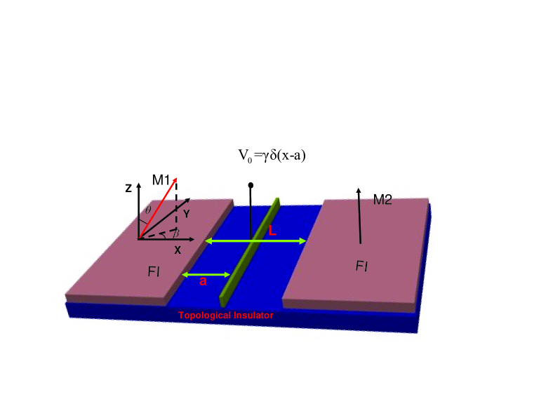
Now, let us consider a ferromagnetic/normal/ferromagnetic tunnel junction which is deposited on the top of a topological surface where a doping potential is exerted on the normal segment. The ferromagnetism is induced due to the proximity effect by the ferromagnetic insulators deposited on the top as shown in Fig. 1. The bulk FI interacts with the electron in the surface of TI by the proximity effect, which is induced a ferromagnetism in the surface of TI. Thus we focus on charge transport at the Fermi level of the surface of TIs, which is described by the 2D Dirac Hamiltonian
| (1) |
where is Pauli matrices , the potential is exerted on the normal segment with where is the position of the potential. In our model, we choose the effective exchange field in the left region with =. We assume that the initial magnetization of FI stripes in the right region is aligned with the +z axis, =. In an actual experiment, one can use a magnet with very strong (soft) easy axis anisotropy to control the ferromagnetic. Because of the translational invariance of the system along direction, the equation admits solutions of the form . We set in the following where is the distance between the two bulk FI as a unit of the length, so the unit of the energy is given with the form . To simplify the notation, we introduce the dimensionless units: , . Due to the presence of the ferromagnet, time-reversal symmetry is broken which can lead to the robustness against disorder. Here, we assume that is shorter than the mean-free path as well as the spin coherence length, so we can ignore the disorder. In order to investigate the doping, we describe the length of the barrier with the potential while keeping =const to replace the potential.
With the above Hamiltonian, wave function in whole system is given by
| (8) |
| (15) |
where , , , , and , , wave vectors in left region and in the right region, respectively. , in the the normal segment. The momentum conservation should be satisfied everywhere. Continuities of the wave function at and , wave functions are connected by the boundary conditions:
| (16) |
which determine the coefficients A,B, and F in the wave functions.
In the liner transport regime and for low temperature, we can obtain the conductance by introducing it as the electron flow averaged over half the Fermi surface from the well-known Landauer-Buttiker formula25,29,30,34, it is straightforward to obtain the ballistic conductance G at zero temperature
| (17) |
where is the width of interface along the y direction, which is much larger than L(), and we take E as , because in our case the electron transport happens around the Fermi level.
III Results and Discussions

In what follows, we use as the unit of the conductance. It is worth noting that we set where is the distance between the two bulk FI as a unit of the length, so the unit of the energy is given with the form .
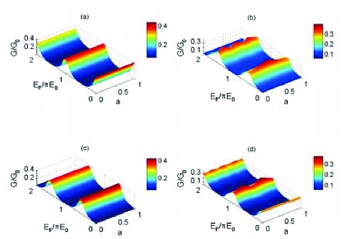
In Fig.2, we show the normalized conductance as a function of the Fermi energy and the doping potential parameter for and . The left panels (a), (c) and (e) correspond to the parallel configuration and the right panels (b), (d) and (f) correspond to the antiparallel configuration. It is easily seen that the conductance oscillates with Fermi energy and the doping potential parameter . The difference of the conductance is very obvious between the negative doping potential parameter and the positive doping potential parameter . It is easily seen that the oscillation period of the conductance against the Fermi energy corresponding to a negative doping potential parameter is smaller than that corresponding to the same value but positive doping potential parameter . It is found that the conductance is the maximum at the parallel configuration while it is minimum at the antiparallel configuration and vice versa, which shows a control of giant magnetoresistance effect [see Fig 2(a) and (b)] as the similar report by Ref. [27,30]. In order to further investigate these effect, we fix the barrier potential parameter to discuss the electronic conductance against the Fermi energy as shown in Fig 2(c) and (d), where the panels (c) and (d) correspond to the parallel configuration and the antiparallel configuration, respectively. We can see that the conductance oscillates with increasing the Fermi energy due to the phase factor and () from Eq. (3), where is the function as the the Fermi energy . These oscillate states may originate from the electron confined in the region between the ferromagnetic segment and doping segment. Also we can easily see that doping change dramatically the conductance. The conductance changes with the Fermi energy in the same way both in Fig. 2(c) and (d). The difference is that the conductance is maximum in Fig. 2(c) while it is minimum in Fig. 2(d), and vice versa. It is more interesting to us, the conductance as the function of the Fermi energy is compressed totally in the antiparallel configuration compared with the parallel configuration, which shows a quantum switch on-off property. In Fig.2 (e) and (f), we discuss the change of the electronic conductance against the doping potential parameter , where the panels (e) and (f) correspond to the parallel configuration and the antiparallel configuration, respectively. The transmission coefficient is rather complicated but we note that it contains the doping parameter only in the form of and , and the transmission probability in a certain Fermi energy can write a general formula as , where all of is the function of the Fermi energy and . We note the fact that , thus we easily understand the fact that the conductance for is not the same to that for unless the Fermi energy where is a integer [see in Fig.2 (c) and (d)]. However, we can note that the transmission probability and hence the conductance are periodic with respect to . It is easily seen that the change of conductance between maximum and minimum by the doping is similar to the spin field-effect transistor, where the modulation of the conductance arises from the spin precession due to spin-orbit coupling [25]. The reason is that the spin direction of wave function rotates through the different regions due to spin-momentum locked. Furthermore, we also note that the conductance is maximum in Fig. 2(e) while it is minimum in Fig. 2(f), and vice versa. It is give us a chance to obtain a large maximum/minimum ratio of the conductance, which is important for a transistor.
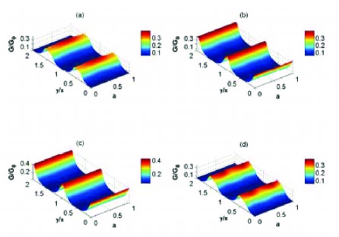
In order to investigate the effect of the position of the doping on the conductance, we show the normalized conductance in Fig.3 as a function of the Fermi energy and the doping position parameter for for the different doping potential parameters [(a) and (c)] and [(b) and (d)] . The panels (a) and (b) correspond to the parallel configuration and the panels (c) and (d) correspond to the antiparallel configuration. It is easily seen that for the fixed doping potential parameters the conductance is maximum in parallel configuration [ see in Fig. 3(a) and (b)] while it is minimum in antiparallel configuration [see in Fig. 3(c) and (d)], and vice versa. For doping potential parameters , there is no doping in the normal segment. Thus the conductance is not change by changing the doping position parameter . It is more interesting to us that the conductance is periodic with respect to the Fermi energy . The reason is that there are some electron state in the normal segment where the electron is confined into it. When the incident wave length in the normal segment satisfies where is integer, quantum interference in the normal segment can enhance the transmitted wave. That is to say, there are some confined state, . When this condition above is satisfied, a peak of conductance can appear. For the antiparallel configuration, we can assume that there is a half wave loss when the incident wave length in the normal segment reflect many times between the two different ferromagnetic layer, which is analogy to the optics reflected in different medius. That is to say, there are some confined state, . When this condition above is satisfied, a peak of conductance will appear. Thus there is energy difference between the Fermi energy corresponding to the peak of the conductance in parallel configuration and that in antiparallel configuration. When the doping appears, the quantum interference condition is change, . So we can easily understand that the conductance is maximum in Fig. 3(a) and (c) where conductance is minimum in Fig. 3(b) and (d) and vice versa. For antiparallel configuration, there is also a half wave loss. Furthermore, we can find that the position of doping in the normal segment can affect the electronic conductance because of the position of doping also induced quantum phase interference in a certain Fermi energy. It is worth noting that a large the Fermi energy mean to a large of the number of confined electron state. Thus, the number of peaks for the large Fermi energy is more than that for the small Fermi energy . The similar results are seen in Fig.4. It is reasonable to us that periodic of the conductance appears as the above analysis. Compared with the parallel configuration, there is also a half-wave loss when the electron wave enter through the antiparallel configuration.
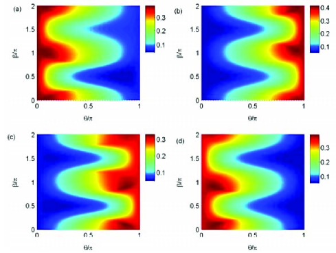
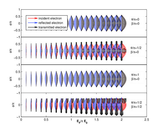
In Fig.5, we show schematic diagram of the normalized conductance with and for (a) and , (b) and , (c) and , and (d) and . The conductance depends sensitively on the direction of the magnetization of the two ferromagnets. It is easily seen that for the fixed doping potential parameters and Fermi energy , in Fig.5 (a) and (c) the conductance is maximum in parallel configuration ( ) while it is minimum in antiparallel configuration (), which similar to the conventional magnetoresistance effect. In Fig. 2 (b) and (d), the conductance takes minimum at the parallel configuration ( )while it takes maximum near antiparallel configuration ( ), which is in stark contrast to the conventional magnetoresistance effect. From these figure, we can see that the half-wave loss also exists when the electron wave enter through the antiparallel configuration according to the analysis above. To understand these results intuitively, we describe the underlying physics in Fig. 6 where the spin orientation of incident( red arrows), transmitted (black arrows) and reflected (blue arrows) are shown. It is well known [1,4,6] that the electron spin is locked in the surface plane in the case of 2D. The spin polarization averaged in the spin space can be shown , . where the normalized wave functions are chosen using the Eq. (2) and (3). It is easily seen that the spin polarization obviously depend on the direction of the magnetization. Thus the conductance depends sensitively on the direction of the magnetization of the two ferromagnets, which originate from the control of the spin flow due to spin-momentum locked.
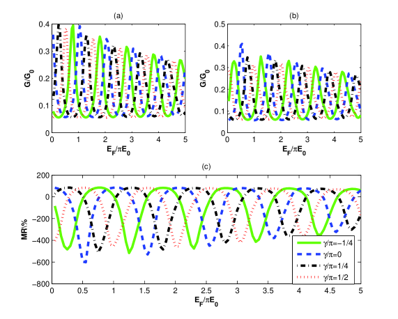
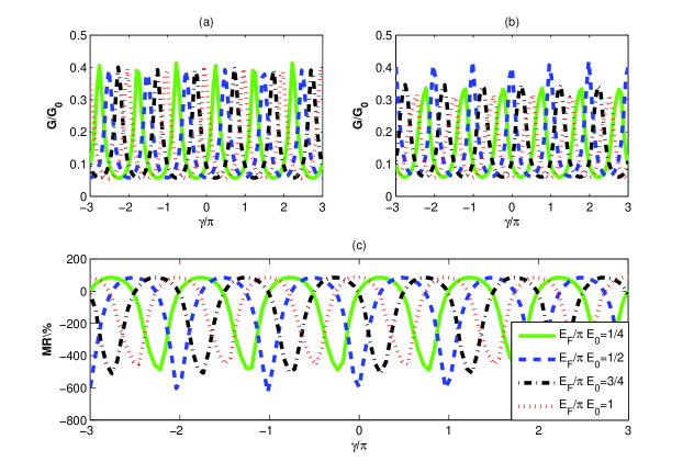
In Fig.7, we show schematic diagram of the normalized conductance [(a) and (b)] and (c) MR as a function of the Fermi energy with and for the different doping potential parameters . The panel (a) corresponds to the parallel configuration, but the panel (b) corresponds to the antiparallel configuration. After obtaining the conductance in the parallel configuration () and the conductance in the antiparallel configuration (),we can define MR as the form: . Both the conductance and MR oscillate with a period as the Fermi energy increases. It is easily seen that the MR could be negative as large as 600% and the maximum of MR can approach 100%. That is to say, the electron conductance obviously change between the parallel configuration and the antiparallel configuration. It is the reason that the giant magnetic resistance effect will produce. From this figure, we can easily see that when the doping potential parameters , the peak of MR increases and the resonant peaks of the MR obviously shift to the higher Fermi energy with increasing of the doping potential parameters . We also can find that by increasing the Fermi energy, the MR oscillatorily decreases and it has the smaller oscillatory magnitude. When the doping potential parameters , the peak of MR increases , then decreases with increasing of the Fermi energy. In Fig.8, the variation of the conductance and the MR are similar to the Fig.7. It is easily seen that the oscillatory magnitude is not change in the negative and the positive , respective. It is because that both the two region the conductance changes with a period. It is also seen that the MR could be negative as big as 600% and the maximum of MR can approach 100%. These characters are very helpful for making new types of MR devices according to the practical applications.
IV Conclusion
In this paper, We have studied the electronic transport properties of the two-dimensional ferromagnetic/normal/ferromagnetic tunnel junction on the surface of a three-dimensional topological insulator with taking into doping account. It is found that the conductance oscillates with the Fermi energy, the position and the aptitude of the doping. Also the conductance depends sensitively on the direction of the magnetization of the two ferromagnets, which originate from the control of the spin flow due to spin-momentum locked. It is found that the conductance is the maximum at the parallel configuration while it is minimum at the antiparallel configuration and vice versa, which may originate from the half wave loss due to the electron wave entering through the antiparallel configuration. Furthermore, we report anomalous magnetoresistance based on the surface of a three-dimensional topological insulator. The MR could be negative as large as 600% and the maximum of MR can approach 100%. That is to say, the electron conductance obviously change between the parallel configuration and the antiparallel configuration. These characters are very helpful for making new types of magnetoresistance devices due to the practical applications.
Acknowledgments: One of authors(J. H. Y) acknowledges discussions with Shi Yu (Guangxi medical university, Nanning, Guangxi, 530021, China ).
References
- (1) M. Z. Hasan and C. L. Kane, Rev. Mod. Phys. 82, 3045 (2010)
- (2) J. E. Moore, Nature (London) 464, 194 (2010)
- (3) L. Fu, C. L. Kane, and E. J. Mele, Phys. Rev. Lett. 98, 106803 (2007)
- (4) D. Hsieh et al.,Nature (London) 452, 970 (2008)
- (5) A. A. Burkov and D. G. Hawthorn, Phys. Rev. Lett. 105, 066802 (2010)
- (6) C. L. Kane and E. J. Mele, Phys. Rev. Lett. 95, 146802 2005
- (7) B. A. Bernevig and S. C. Zhang, Phys. Rev. Lett. 96, 106802 2006
- (8) C. Wu, B. A. Bernevig, and S. C. Zhang, Phys. Rev. Lett. 96, 106401 2006
- (9) C. Xu and J. E. Moore, Phys. Rev. B 73, 045322 2006
- (10) L. Fu and C. L. Kane, Phys. Rev. B 76, 045302 (2007)
- (11) X.-L. Qi, T. L. Hughes, and S.-C. Zhang, Phys. Rev. B 78, 195424 (2008)
- (12) B. A. Bernevig, T. L. Hughes, and S. C. Zhang, Science 314, 1757 (2006)
- (13) M. König, S. Wiedmann, C. Br ne, A. Roth, H. Buhmann, L. Molenkamp, X.-L. Qi, and S.-C. Zhang, Science 318, 766 (2007)
- (14) J. E. Moore and L. Balents, Phys. Rev. B 75, 121306(R) (2007)
- (15) L. Fu, C. L. Kane, and E. J. Mele, Phys. Rev. Lett. 98, 106803 (2007)
- (16) J. C. Y. Teo, L. Fu, and C. L. Kane, Phys. Rev. B 78, 045426 (2008)
- (17) H. Zhang et al., Nature Phys. 5, 438 (2009)
- (18) T. Eguchi, P. Gilkey, and A. Hansen, Phys. Rep. 66, 213 (1980)
- (19) E. I. Rashba, Sov. Phys. Solid State 2, 1109 (1960); Yu. A. Bychkov and E. I. Rashba, J. Phys. C 17, 6039 (1984)
- (20) D. Hsieh, Y. Xia, L. Wray, D. Qian et al, Science 323, 919 (2009)
- (21) A. Nishide, A. Taskin, Y. Takeichi, T. Okuda, A. Kakizaki, T. Hirahara, K. Nakatsuji, F. Komori, Y. Ando, and I. Matsuda, Phys. Rev. B 81, 041309 (2010)
- (22) Q. Liu, C. X. Liu, C. Xu, X. L. Qi, and S. C. Zhang, Phys. Rev. Lett. 102, 156603 (2009)
- (23) X. L. Qi, R. D. Li, J. D. Zang, and S. C. Zhang, Science 323, 1184 (2009)
- (24) X. L. Qi, T. L. Hughes, and S. C. Zhang, Phys. Rev. B 78, 195424 (2008)
- (25) S. Datta and B. Das, Appl. Phys. Lett. 56, 665 (1990)
- (26) A. Fert, Rev. Mod. Phys. 80, 1517 (2008)
- (27) Xiaolin Wang, Yi Du, Shixue Dou, and Chao Zhang, Phys. Rev. Lett. 108, 266806 (2012)
- (28) B. Xia, P. Ren, Azat Sulaev, Z. P. Li, P. Liu, Z. L. Dong, and L. Wang, Advances 2, 042171 (2012)
- (29) B. D. Kong, Y. G. Semenov, C. M. Krowne, and K. W. Kim, Appl. Phys. Lett. 98, 243112 (2011)
- (30) T. Yokoyama, Y. Tanaka, and N. Nagaosa, Phys. Rev. B 81, 121401(R) (2010);KH Zhang, ZC Wang, QR Zheng, G Su, Phys. Rev. B 86, 174416 (2012)
- (31) S. Mondal, D. Sen, K. Sengupta, and R. Shankar, Phys. Rev. Lett. 104, 046403 (2010); Phys. Rev. B 82, 045120 (2010)
- (32) Z. Wu, F. M. Peeters, and K. Chang, Phys. Rev. B 82, 115211 (2010)
- (33) Y. Zhang and F. Zhai, Appl. Phys. Lett. 96, 172109 (2010)
- (34) Jianhui Yuan, Yan Zhang, Jianjun Zhang and Ze Cheng Eur. Phys. J. B 86, 36 (2013); J. P. Zhang and J. H. Yuan, Eur. Phys. J. B 85, 100 (2012)
- (35) A. Matulis, F. M. Peeters, and P. Vasilopoulos, Phys. Rev. Lett. 72, 1518 (1994)
- (36) S. J. Lee, S. Souma, G. Ihm, and K. J. Chang, Phys. Rep. 394, 1 (2004)
- (37) M. Cerchez, S. Hugger, T. Heinzel, and N. Schulz, Phys. Rev. B 75, 035341 (2007)