Effect of spin-orbit interaction on the excitonic effects in single-layer, double-layer, and bulk MoS2
Abstract
We present converged ab-initio calculations of the optical absorption spectra of single-layer, bi-layer, and bulk MoS2. Both the quasiparticle-energy calculations (on the level of the GW approximation ) and the calculation of the absorption spectra (on the level of the Bethe-Salpeter equation) explicitly include spin-orbit coupling, using the full spinorial Kohn-Sham wave-functions as input. Without excitonic effects, the absorption spectra would have the form of a step-function, corresponding to the joint-density of states of a parabolic band-dispersion in 2D. This profile is deformed by a pronounced bound excitonic peak below the continuum onset. The peak is split by spin-orbit interaction in the case of single-layer and (mostly) by inter-layer interaction in the case of double-layer and bulk MoS2. The resulting absorption spectra are thus very similar in the three cases but the interpretation of the spectra is different. Differences in the spectra can be seen around 3 eV where the spectra of single and double-layer are dominated by a strongly bound exciton.
pacs:
73.22.-f, 78.20.Bh, 78.67.WjI Introduction
The promising and interesting physical properties of graphenenovoselov have recently stimulated active research in other atomically thin materials, alternative and/or complementary to graphene.coleman Molybdenum disulfide (MoS2), fabricated in its single-layer by means of mechanical exfoliation, exhibits a direct bandgap of 1.8-1.9 eV, contrary to the indirect band gap of its bulk counterpart.splendiani2010 ; mak2010 Moreover, single-layer MoS2 has also shown a mobility of 200 cmVs which makes it appealing for the design of a new generation of more efficient transistors.kis2011 In the field of spintronics, the absence of inversion symmetry in the crystal structure of single-layer MoS2 allows valley polarization by optical pumping with circularly polarized light.yao2008 ; xiao2012 This makes possible the design of devices based on spin and valley control.zeng2012 ; mak2012 More recently, a remarkable Seebeck coefficient has been measured in single-layer MoS2, opening a new field of application for those materials.castellanos2013 Concerning the optical properties, the photoluminescence in single-layers has shown higher efficiency than in multi-layers or bulk which is attributed to the direct/ indirect band-gaps, respectively. The absorption spectra however are very similar in all the cases,splendiani2010 ; mak2010 ; castellanos2011 an issue not yet explained. The observed double-peak structure in the absorption spectra can be connected to the splitting of the valence band maximum around the high-symmetry point . For single-layer MoS2, this splitting was explained as a consequence of spin-orbit coupling which is a result of the missing inversion symmetry.zhu11 For bilayer and bulk, this splitting is mainly due to inter-layer interaction.lambrecht2012
In this context, reliable ab initio calculations of the absorption spectra are necessary for providing the correct interpretation of the reported experimental results. However, the inherent complexity of the Bethe-Salpeter equationonida2002 that is usually used to describe the excitonic effects in the optical spectra seems to be the reason for recent inadequately converged calculations. In Ref. rama, the excitonic binding energy is strongly overestimated due to a low k-point sampling and in Refs. singh, and feng12, spin-orbit interaction was entirely neglected and the splitting of the excitonic peak is merely due to an unconverged k-point sampling. The aim of our work is to provide well-converged optical spectra, in the framework of the Bethe-Salpeter equation including the effects of spin-orbit coupling. This gives a reliable basis for the interpretation of previous experimental works on single-, double-layer and bulk MoS2. We show that the the optical spectrum corresponds essentially to a step-function that is the result of the joint-density of states for parabolic dispersion in two-dimensional systems. Excitonic effects shift part of the oscillator strength into a discrete excitonic peak below the continuum onset. The splitting of this excitonic peak can be directly related to the splitting of the valence band maximum around and is thus entirely due to spin-orbit coupling in the case of the single-layer and mostly (but not entirely) due to inter-layer interaction for double, and multi-layer MoS2.
II Calculation Methods
Starting point of the calculation of optical spectra are the Kohn-Sham wave functions and energies calculated with density-functional theory (DFT) in the local-density approximation (LDA). We use the code ABINITgonze2002 where wave-functions are expanded in plane-waves and core electrons are simulated by norm-conserving relativistic pseudopotentials.hgh The plane-wave energy cutoff is 30 a.u. For Molybdenum, the 4s and 4p semi-core electrons are explicitly calculated (in addition to the 4d and 5s valence electrons). This turns out to be crucial for the proper calculation of the exchange-contribution to the self-energy term in the GW calculations. As noted earlier,zhu11 ; lambrecht2012 spin-orbit interaction is important for MoS2 and we calculate the spinor-wavefunctions as input for the following calculations on the level of many-body perturbation theory.
The inherent underestimation of the bandgap given by DFT is corrected with the GW method.hedin1970 ; onida2002 We use the non-self consistent version (denoted as G0W0) without updating the dielectric function in the screened Coulomb potential (W) or the wave-functions and energies in the Green’s function (G). These calculations are done with the Yambo code.yambo The dielectric function is calculated using the plasmon-pole approximationppa_note . 50 G-vectors are used (for a vacuum distance of 40 a.u. between the periodic images of the single-layer/double-layer calculations). 200 unoccupied bands are used in the integration of the self-energy term, yielding converged band-gap corrections for single-layer, double-layer, and bulk. The -point sampling is for single and double-layer and for bulk. The value of the GW-correction to the band-gap depends on the inter-layer distance in the periodic supercells approach. It increases with increasing distance and converges roughly as (where is the supercell dimension perpendicular to the layer). This was shown for single layers of hexagonal boron nitride (hBN)wirtz2006 and for single-layers of MoS2.komsa At the same time, the excitonic binding energy was also shown to increase roughly as such that the two effects cancel and the resulting optical spectra hardly depend on the inter-layer distance. In our calculations, we use a.u. for the single layer calculations and of a.u. for the double-layer.
Starting from the Kohm-Sham wave-functions and the quasi-particle energies, the optical-spectra are calculated on the level of the Bethe-Salpeter equation (BSE):strinati82 ; strinati84 ; rohlfing2000 ; palummo2004
| (1) |
Here, the electronic excitations are expressed in the basis of electron-hole pairs (i.e., vertical excitations at a given -point from a state in the valence band with quasi-particle energy to a conduction-band state with energy . The are the expansion coefficients of the excitons in the electron-hole basis and the are the eigenenergies (corresponding to the possible excitation energies of the system). If the interaction kernel is absent, Eq. (1) simply yields , i.e., the excitations of the system correspond to independent electron-hole pairs. The interaction kernel describes the screened Coulomb interaction between electrons and holes, and the exchange interaction, which includes the so called local fields effect. “mixes” different single-particle excitations, from valence band states to conduction band states , giving rise to modified transition energies and (possibly) also to discrete excitonic states below the onset of the continuum.
The optical absorption spectrum is given by the imaginary part of the dielectric function, , and can be calculated as
| (2) |
where are the dipole matrix elements for electronic transitions from valence to conduction states. We consider only light absorption with polarization, and thus the direction of the dipole operator , in the plane identified by the layer. The out-of-plane polarization gives negligible contribution to absorption at low energies, because the local fields, which are strongly inhomogeneous in that direction, shift the oscillator strength to high energies. Excluding phonon-assisted transitions, the momentum is conserved in the absorption process. We use an energy broadening eV in all the calculations to mimic the experimental resolution. The BSE calculations have been performed with the code Yambo.yambo Since a much higher -point sampling than for the GW-calculations is needed, we use LDA wave-functions and energies, corrected by a “scissor”-operator obtained from the GW-calculations. While this approach does not take into account changes in the valence and conduction band dispersions, we have checked for the excitonic spectrum at a sampling of (single-layer) that the difference to a BSE-calculation based on GW-energies is negligible.
III Quasi-particle band-structure
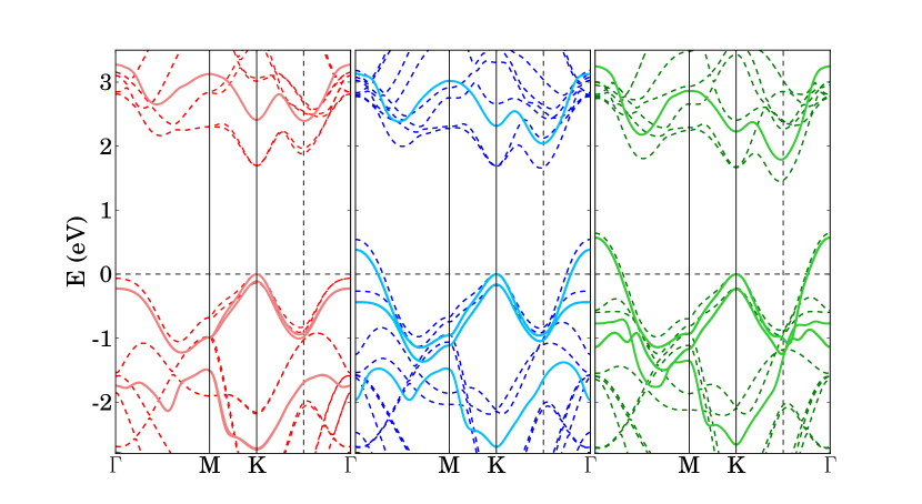
First we study the electronic structure of single-layer, double-layer and bulk MoS2. It is worth to mention that an accurate calculation of the exchange interaction in both the GW approximation and the BSE requires the use of semi-core (4s and 4p) orbitals for the molybdenum atoms. The omission of semi-core states can lead to an erroneous wave-vector dependence of the GW-correction. Furthermore, the spin-orbit interaction has to be taken into account because it removes the degeneracy of the valence band maximum. Single-layer MoS2 (and, in general, odd number of layers) belongs to the group of symmetry ,alex which lacks inversion symmetry. This absence of symmetry, together with the strong spin-orbit coupling of molybdenum orbitals, splits the valence band edge at .xiao2012 MoS2 with even number of layers, such as the double-layer, and the bulk, instead, belong to the symmetry group , which does have inversion symmetry. Nevertheless, also in this case a valence band splitting exists but it is caused (predominantly) by the interlayer interaction.
Figure 1 shows the band structure, calculated with LDA and GW, for single-, double-layer and bulk MoS2. The only case where a direct bandgap is observed is the single-layer, either in LDA or in GW, while for double-layer and bulk the bandgap is clearly indirect. The origin of this difference is the interlayer interaction. A second minimum in the conduction band lies on the high-symmetry line between and (see vertical dashed lines). For the single-layer, this minimum is higher in energy than the one at but in the double-layer and bulk, the inter-layer interaction leads to a splitting which shifts the minimum to a lower energy than the minimum at . Moreover, in the double-layer and in the bulk, the valence band edge at rises higher than the valence band maximum at . As a consequence the system moves from a direct band-gap to an indirect gap semi-conductor. The GW corrections are generally larger for single-layer MoS2 then for the double-layer and the bulk, due to the smaller dielectric screening in the single-layer case.
Our band-structures and their interpretation agree very well with the ones of the recent self-consistent GW calculations,lambrecht2012 even though details in the approximations are different: in our study, we do not use self-consistency in the GW-calculations which seems to add only a minor energy-shift to the G0W0 calculation. In turn, we perform the GW calculations with the full spinor wave-functions while in Ref.lambrecht2012, spin-orbit coupling is introduced after the GW-calculations by rediagonalizing the Hamiltonian matrices. The values of the direct band gaps at are summarized in Table 1, combined with the valence band splitting. The values are in reasonable agreement with the ones of Ref. lambrecht2012, . Small differences may be due to the differences in the approximations and from the different values of the cell dimensions.
We remark in this context the importance of the lattice constant. Small variations of the latter can shift the position of the conduction and valence band edges. Commonly to other GW calculations, we thus use experimental lattice parameters (in-plane lattice constant a=3.15 Å and c=12.3 Å for bulknicklow ) in order to avoid artificial strain effects.rinke2007 A similar conclusion is drawn in a recent theoretical study about the influence of strain in the bandgap of MoS2, where strain tends to transform the single-layer MoS2 into an indirect band-gap semiconductor.mattheis1973 ; yun2012
| Material parameters | |||
|---|---|---|---|
| 1-layer | 2-layer | Bulk | |
| (LDA) | 1.69 | 1.68 | 1.67 |
| (GW) | 2.41 | 2.32 | 2.23 |
| (LDA) | 134.3 | 173.8 | 220.1 |
| (GW) | 112.0 | 160.0 | 230.6 |
IV Optical absorption spectra
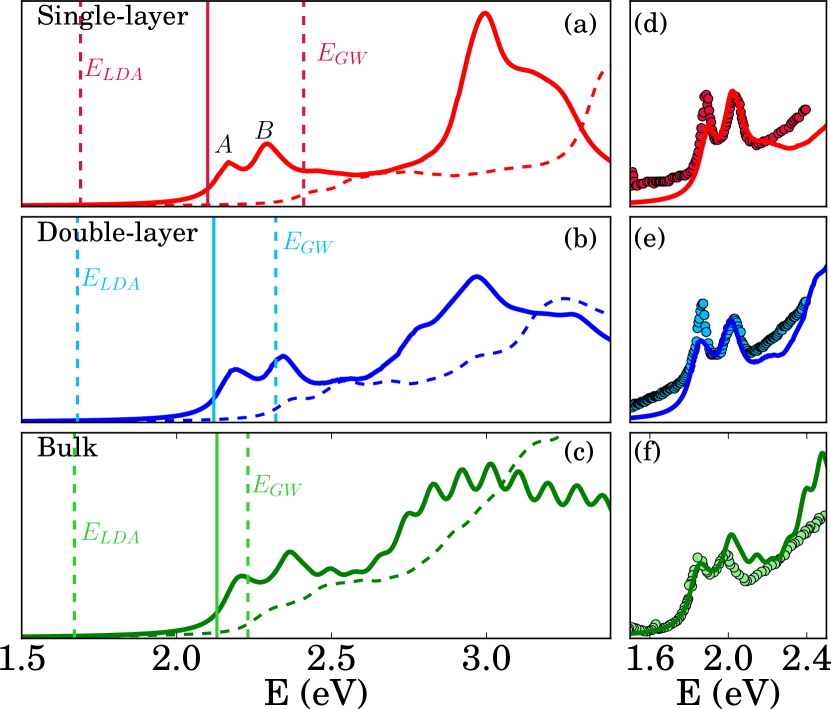
In the calculation of the optical absorption spectra of MoS2, the convergence with respect to -sampling is of crucial importance in order to obtain reliable spectra (see Appendix). We used a k-point in the case of the single-layer and double-layer and in the case of bulk. Local fields are included in all the calculations.speedup We show in Fig. 2, the calculated optical spectra for single-, double-layer and bulk MoS2. The results of the BSE are compared with the optical spectra without the excitonic effects, calculated in the random-phase approximation (RPA, independent-particle picture) using the GW-energies (Panels a-c). The LDA and GW band-gap energies are marked with vertical. Finally (Panels d-f) the BSE results are compared with the experimental datasplendiani2010 ; mak2010 . In panels d-f the theoretical results are down-shifted by approximately 0.2 eV in order to compare with the experiments. This discrepancy is in the margin error of common GW and Bethe-Salpeter calculations. Our results give a clear interpretation of the measured absorption spectra, in the low energy range, and provide reliable predictions within the given accuracy of 0.2 eV, for the higher energy range, for which no experimental data are available.
The general features of the three optical spectra are very similar, with a double peak structure (denoted as and ) at the energy threshold, accompanied by a plateau, and afterwards an abrupt increase of the optical absorption. The RPA spectrum below 2.8 eV resembles in all three cases the sum of two Heaviside step functions. The difference in the two step positions is given by the splitting of the valence band maximum at . This step function profile is the fingerprint of the joint density of states of a 2D-system, with parabolic band structure. “Switching on” excitonic effects, preserves the plateau, but, in addition, a split excitonic peak below the onset of the continuum transition occurs. The exciton binding energy is different in the three cases. It is largest for the single-layer, where the electron-hole interaction is less screened. The differences in quasi-particle band gap and excitonic binding energy almost cancel each otherwirtz2006 ; komsa and the resulting excitonic peak positions are almost the same in the three cases. The peaks can be directly assigned to the peaks denoted and in the experiments.mak2010 ; splendiani2010 At higher energies, the relevant peak placed at 3.0 eV (close to the blue color in the visible spectrum) in the single-layer has larger relative intensity with respect to the peaks and . Such intense peak has not yet been reported, as the maximum detection energy in absorption experiments is around 2.4 eV.plechinger2011
A further inspection of the excitonic eigenvectors allows to assign to each excitonic peak the contributing electron-hole transitions and their location at the Brillouin zone. In all the cases, excitons and come from the energy transition at the point, even when the band gap is indirect. This explains the similarity of the experimental optical absorption. The other relevant peak, at 3.0 eV, comes from the part of the Brillouin zone between and (marked with a dashed line in Fig. 1), where we observe a high density of states due to the parallel conduction and valence bands.cardona
To gain further insight of the optical spectra, we represent the excitonic wavefunctions related to the main peaks of the Bethe-Salpeter spectra. The excitonic wave-function can be written as:
| (3) |
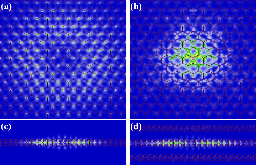
where and are the real-space electron and hole coordinate and the LDA wave functions. The coefficients are obtained by diagonalizing the Hamiltonian of the Bethe-Salpeter equation (with energy ). In order to represent the six-coordinate function, we fix the hole position 1.0 Å above a molybdenum atom and we project onto the function onto the x-y plane. Figure 3(a) shows the exciton wave function of the exciton of the MoS2 single-layer (for double-layer and bulk the wave function is essentially identical). This exciton is largely spread, extended over 65 Å, in concordance with the small binding energy and with the small effect on the absorption threshold, as reported in the experiments.mak2010 ; splendiani2010 This also explains the large -point grid needed to converge the results in the Bethe-Salpeter equation (see Appendix). The exciton (not shown here) shows similar trends.
On the opposite, in Fig. 3(b) we observe that the brightest exciton, at 3.0 eV, is remarkably localized, being confined to less than 30 Å, with a trigonal shape. Among the properties of such exciton we point out the potentially high efficiency of recombination.
Another interesting point (for multi-layer and bulk) is to explore if the excitons are confined in one layer or if their wavefunctions extend over several layers. With this aim we show in Fig. 3(d) the exciton of the MoS2 bulk. The wave function spreads largely within the plane but it is undoubtedly constricted to one layer. The density in neighboring layers is negligible and the wave-function is very similar to the one of the exciton in the single layer (Fig. 3(c)). The large interlayer distance, due to the weak van der Waals interaction, prevents the wave function from spreading to other layers, analogously to what happens in bulk boron nitride.arnaud ; wirtz2011
V Conclusions
We have performed calculations of the quasi-particle band-structure and of the optical absorption spectra of single, double-layer, and bulk MoS2 including excitonic effects and spin-orbit coupling at the same time. In agreement with previous calculations and with experimental evidence from photoluminescence intensities,mak2010 ; splendiani2010 ; sallem2012 our GW-calculations demonstrate that only single-layer MoS2 has a direct band gap at . The inter-layer interaction makes the band gap indirect for multi-layer and bulk Mo. However, this does not particularly influence the optical absorption spectra in the visible range. These display in all cases a strong excitonic peak (composed of electron-hole pairs around ) below the onset of continuum transitions which has the step function shape, corresponds to the quasi-2D joint-density of states. The layered-structure of the material confines the first exciton mostly in a single-layer which causes the similarity of the optical spectrum in all the cases. The position of the split excitonic peak is remarkably stable with respect to the number of layers (and with respect to the inter-layer spacing in the calculation for single-layer MoS2). This has been previously explained as a cancellation effect between the band-gap correction due to electron-electron interaction and the excitonic binding energy due to electron-hole interactionwirtz2006 ; komsa . The splitting of the excitonic peak is directly related to the splitting of the valence band maximum around and is entirely due to spin-orbit coupling for the single-layer and (mostly) due to inter-layer interaction for the double-layer and bulk. At higher energy (around 3 eV), the optical spectrum is dominated by electron-hole pairs from transitions around the center of the line where both valence and conduction bands have a minimum and the parallel shape of the bands causes a maximum in the joint density-of-states. For the single-layer a strongly-bound exciton causes an additional peak in the spectrum at 3.0 eV. For double-layer and bulk, the shape of the spectrum changes and may allow for a spectroscopic distinction between layer numbers.
VI Acknowledgments
The authors acknowledges financial support from the ANR (French National Research Agency) through project ANR-09-BLAN-0421-01. Calculations were done at the IDRIS supercomputing center, Orsay (Proj. No. 091827), and at the Tirant Supercomputer of the University of Valencia (group vlc44).
Appendix A
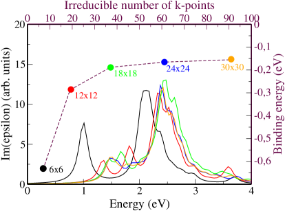
The convergence of the optical spectra is a mandatory issue to obtain reliable spectra, comparable with the experimental data. We have performed calculations to check the convergence of the spectra, and in particular of the position of the first excitonic peak with respect to the -point sampling. A fine sampling can be quite costly in terms of computation time and in some Bethe-Salpeter calculations may reach unexpectedly large values. Figure 4 shows the Bethe-Salpeter spectra of MoS2 single-layer for several -grids (for simplicity we have omitted the spin-orbit coupling). Additionally, we have represented the exciton binding energy, , as a function of the number of irreducible -points, marking in each case the corresponding grid. We observe the slow convergence of the first excitonic peak, not reached before a sampling. Moreover, for small grids some secondary and artificial peaks appear in the spectrum and the underlying Heaviside function of the optical absorption is not reached unless dense grids are used (). This value is considerably larger than the one used in Ref rama, where only a grid was used, leading to isolated peaks in the absorption spectra where the density of states predicts a plateau following the excitonic peak. Our test calculations also explain why in Refs. singh, and feng12, split excitonic peaks were observed even though spin-orbit coupling was not included.
The exciton binding energy also needs at least an grid to be converged within 0.1 eV. It is worth to note that the second excitonic peak (the most intense), located at 2.5 eV converges much faster, approximately for a grid. The difference behavior of those excitons can be better understood by inspection of their wave functions, shown in Fig. 3(a) and (b). In the case of the first peak, the wave function is very spread, more than 18 unit cells in each direction on the plane. We remind that a grid in the reciprocal space allows only to map the exciton wave function in the real space the unit cell, therefore, inadequately small grids lead to an artificial confinement of the exciton which increases its binding energy. This arguments also clarifies why the second exciton converge much faster, its wave function being confined within a few unit cells.
References
- (1) K. Novoselov, D. Jiang, F. Schedin, T. Booth, V. Khotkevich, S. Morozov, and A. Geim, Proc. Natl. Acad. Sci U. S. A. 30, 10451 (2005).
- (2) J. N. Coleman et. al., Science 331, 568 (2011).
- (3) A. Splendiani, L. Sun, Y. Zhang, T. Li, J. Kim, C. Y. Chim, G. Galli, and F. Wang, Nano Lett. 10, 1271 (2010). ngel
- (4) K. F. Mak, C. Lee, J. Hone, J. Shan, and T. F. Heinz, Phys. Rev. Lett. 105, 136805 (2010).
- (5) B. Radisavljevic, A. Radenovic, J. Brivio, V. Giacometti, and A. Kis. Nat. Nanotech. 6, 147 (2011).
- (6) W. Yao, D. Xiao, and Q. Niu, Phys. Rev. B 77, 235406 (2008).
- (7) D. Xiao, G. B. Liu, W. Feng, X. Xu, and W. Yao, Phys. Rev. Lett. 108, 196802 (2012).
- (8) H. Zeng, J. Dai, W. Yao, D. Xiao, X. Cui, Nat. Nanotech. 7, 490 (2012).
- (9) K. F. Mak, K. He, J. Shan, and T. F. Heinz, Nat. Nanotech. 7, 494 (2012).
- (10) M. Buscema, M. Barkelid, V. Zwiller, H. S. J. van der Zant, G. A. Steele, and A. Castellanos-Gomez, Nano Lett. (2013)
- (11) A. Castellanos-Gomez, M. Barkelid, A. M. Goossens, V. E. Calado, H. S. J. van der Zant, and G. A. Steele, Nano Lett. 12, 3187 (2012).
- (12) Z. Y. Zhu, Y. C. Cheng, and U. Schwingenschlögl, Phys. Rev. B 84, 153402 (2011).
- (13) T. Cheiwchanchamnangij and W. R. L. Lambrecht, Phys. Rev. B 85, 205302 (2012);
- (14) T. Korn, S. Heydrich, M. Hirmer, J. Schmurtzler, and C. Schüller, Appl. Phys. Lett. 99, 102109 (2011).
- (15) G. Onida, L. Reining, and A. Rubio, Rev. Mod. Phys. 74, 601 (2002).
- (16) A. Ramasubramaniam, Phys. Rev. B 86, 115409 (2012).
- (17) N. Singh, G. Jabbour, and U. Schwingenschlögl, Eur. Phys. J. B 85, 392 (2012).
- (18) J. Feng, X. Qian, C.-W. Huang, and J. Li, Nat. Phot. 6, 866 (2012).
- (19) X. Gonze et al., Comp. Mat. Sci. 25, 478 (2002).
- (20) C. Hartwigsen, S. Goedecker, and J. Hutter, Phys. Rev. B 58, 3641 (1998).
- (21) L. Hedin and S. Lundqvist, Solid State Phys. 23, 1 (1970).
- (22) The exact position of the pole in this model is not important. Moving the pole leads to differences of less than 5 meV.
- (23) A. Marini, C. Hogan, M. Grüning, and D. Varsano, Comp. Phys. Comm. 180, 1392 (2009); http://www.yambo-code.org.
- (24) L. Wirtz, A. Marini, and A. Rubio, Phys. Rev. Lett. 96, 126104 (2006).
- (25) H.P. Komsa and A. V. Krasheninnikov, Phys. Rev. B 86, 241201(R), 2012.
- (26) G. Strinati, Phys. Rev. Lett. 49, 1519 (1982).
- (27) G. Strinati, Phys. Rev. B 29, 5718 (1984).
- (28) M. Rohlfing and S. G. Louie, Phys. Rev. B 62, 4927 (2000).
- (29) M. Palummo, O. Pulci, R. Del Sole, A. Marini, P. Hahn, W. G. Schmidt, and F. Bechstedt, J. Phys.: Condens. Matter 16, S4313 (2004).
- (30) A. Molina-Sánchez and L. Wirtz, Phys. Rev. B 84, 155413 (2011).
- (31) N. Wakabayashi, H. G. Smith, and R. M. Nicklow, Phys. Rev. B 12, 659 (1975).
- (32) P. Rinke, M. Winkelnkemper, A. Qteish, D. Bimberg, J. Neugebauer, and M. Scheffler, Phys. Rev. B 77, 075202 (2008).
- (33) L. F. Mattheiss, Phys. Rev. B 8, 3719 (1973).
- (34) W. S. Yun, S. W. Han, S. C. Hong, I. G. Kim, and J. D. Lee, Phys. Rev. B 85, 033305 (2012).
- (35) In order to speed up the calculation to obtain smooth spectra, we have also tested the double-grid method proposed in Ref. kammer, . In this case a basic grid of for single-layer and double-layer yields almost the same results as the grid.
- (36) D. Kammerlander, S. Botti, M. A. L. Marques, A. Marini, and C. Attaccalite, Phys. Rev. B 86, 125203 (2012).
- (37) G. Plechinger, F.-X. Schrettenbrunner, J. Eroms, D. Weiss, C. Schüller, and T. Korn, Phys. Status Solid RRL 6, 128 (2012).
- (38) M. Cardona and P. Y. Yu, Fundamentals of Semiconductors (Springer-Verlag, Berlin, 1996).
- (39) B. Arnaud, S. Lebègue, P. Rabiller, and M. Alouani, Phys. Rev. Lett. 96, 026402 (2006).
- (40) S. Galambosi, L. Wirtz, J. A. Soininen, J. Serrano, A. Marini, K. Watanabe, T. Taniguchi, S. Huotari, A. Rubio, and K. Hämäläinen, Phys. Rev. B 83, 081413(R) (2011).
- (41) A. Kokalj, Comp. Mater. Sci. 28, 155 (2003), http://www.xcrysden.org/.
- (42) G. Sallen, L. Bouet, X. Marie, G. Wang, C. R. Zhu, W. P. Han, Y. Lu, P. H. Tan, T. Amand, B. L. Liu, and B. Urbaszek, Phys. Rev. B 86, 081301R (2012).