Effect of a built-in electric field in asymmetric ferroelectric tunnel junctions
Abstract
The contribution of a built-in electric field to ferroelectric phase transition in asymmetric ferroelectric tunnel junctions is studied using a multiscale thermodynamic model. It is demonstrated in details that there exists a critical thickness at which an unusual ferroelectric-“polar non-ferroelectric”phase transition occurs in asymmetric ferroelectric tunnel junctions. In the “polar non-ferroelectric”phase, there is only one non-switchable polarization which is caused by the competition between the depolarizing field and the built-in field, and closure-like domains are proposed to form to minimize the system energy. The transition temperature is found to decrease monotonically as the ferroelectric barrier thickness is decreased and the reduction becomes more significant for the thinner ferroelectric layers. As a matter of fact, the built-in electric field does not only result in smearing of phase transition but also forces the transition to take place at a reduced temperature. Such findings may impose a fundamental limit on the work temperature and thus should be further taken into account in the future ferroelectric tunnel junction-type or ferroelectric capacitor-type devices.
I INTRODUCTION
Ferroelectric (FE) tunnel junctions (FTJs) that are composed of FE thin films of a few unit cells sandwiched between two electrodes (in most cases the top and bottom electrodes are different) have attracted much more attention during the last decade. Tsymbal ; KOHLSTEDT ; Zhuravlev It is generally believed that the interplay between ferroelectricity and quantum-mechanical tunneling plays a key role in determining tunnel electroresistance (TER) or tunneling current and TER effect usually takes place upon polarization reversal. Due to the strong coupling of FE polarization and the applied field, the electric-field control of TER or tunneling current, Tsymbal ; KOHLSTEDT ; Zhuravlev ; Garcia0 ; Garcia1 ; Garcia2 ; VELEV ; Bilc ; PANTEL ; Gruverman ; Chanthbouala spin polarization, Zhuravlev1 ; Duan ; Sahoo ; Duan1 ; Niranjan ; Burton ; VELEV1 ; Zhuravlev2 ; Garcia3 ; Hambe ; Valencia ; Meyerheim ; Bocher ; Lu1 ; PANTEL1 and electrocaloric effect Liu can be achieved, which makes FEs promising candidates for nondestructive FE storage, Tsymbal ; KOHLSTEDT ; Zhuravlev ; Garcia0 ; Garcia1 ; Garcia2 ; VELEV ; Bilc ; PANTEL ; Gruverman FE memristor, Chanthbouala spintronics (magnetization), Zhuravlev1 ; Duan ; Sahoo ; Duan1 ; Niranjan ; Burton ; VELEV1 ; Zhuravlev2 ; Garcia3 ; Hambe ; Valencia ; Meyerheim ; Bocher ; Lu1 ; PANTEL1 or electrocaloric Liu devices. Meanwhile, another mechanically (including strain or strain gradient) induced TER is found recently, which also shows their potential applications in mechanical sensors, transducers and low-energy archive data storage decices. Luo Note that having different electrodes for the FTJs (some experiments use conductive atomic force microscope tips instead of the top electrodes) is usually required for a large effect at low bias voltage though the FTJs with same electrodes may also display interesting performances. KOHLSTEDT ; VELEV ; VELEV1 ; Bilc Also note that all the functionalities in these devices are strongly related to the thermodynamic stability and switching ability of FTJs. Tsymbal ; KOHLSTEDT ; Zhuravlev ; Garcia0 ; Garcia1 ; Garcia2 ; VELEV ; VELEV1 ; Bilc ; PANTEL ; Gruverman ; Garcia3 ; Hambe ; PANTEL1 ; Luo ; Chanthbouala ; Zhuravlev1 ; Duan ; Sahoo ; Duan1 ; Niranjan ; Burton ; VELEV1 ; Zhuravlev2 ; Garcia3 ; Hambe ; Valencia ; Meyerheim ; Bocher ; Lu1 ; PANTEL1 ; Liu Therefore, a fundamental understanding of ferroelectricity of FTJs, especially their size effects, is crucial at the current stage of research.
Unfortunately, no consensus has been achieved on whether there exists a critical thickness below which the ferroelectricity disappears in FTJs, especially for those with different top/bottom electrodes. It is believed that an electrostatic depolarizing field caused by dipoles at the FE-metal interfaces is responsible for the size effect. Mehta ; Junquera ; Kim ; Pertsev ; Gerra0 ; Tagantsev However, recent theoretical studies suggest that the choice of electrode material may lead to smearing of size effect or even vanishing of . Stengel ; Zheng0 ; Zheng1 ; Cai0 ; Cai1 For example, it was reported that choosing Pt as electrodes would induce a strong interfacial enhancement of the ferroelectricity in Pt/BaTiO3(BTO)/Pt FTJs, where is only 0.08 BTO unit cell. Stengel In addition, the results of a modified thermodynamic model Zheng0 ; Zheng1 and first-principles calculations Cai0 ; Cai1 both indicate that BTO barrier with dissimilar electrodes, i.e. Pt and SrRuO3 (SRO) electrodes, might be free of deleterious size effects. In contrast, it has been reported that asymmetric combination of the electrodes (including the same electrodes with different terminations) will result in the destabilization of one polarization state making the asymmetric FTJs non-FE. Gerra0 ; UMENO And the up-to-date studies reported that the fixed interface dipoles near the FE/electrode interface is considered the main reason for that detrimental effect. LIU ; LU Considering the importance of the physics in FTJs with dissimilar top and bottom electrodes, we are strongly motivated to investigate the size effect in such asymmetric FTJs.
It was pointed out as early as 1963 that the contribution of different electronic and chemical environments of the asymmetric electrode/FE interfaces would induce a large long-range electrostatic built-in electric field in FE thin films. Simmons becomes more significant in asymmetric FTJs and should be taken in to account. Gerra0 ; Tagantsev In this study, we use a multiscale thermodynamic model Liu ; Gerra0 ; Tagantsev to investigate the effect of such built-in electric field on the phase transition of asymmetric FTJs by neglecting the short-range interface dipoles. As a result, we discover an unusual FE-“polar non-FE”phase transition in asymmetric FTJs. Then, we make detailed analysis of the contribution of the built-in electric field to FE phase transition, i.e. , what happens below , transition temperature , and temperature dependence of dielectric response of the asymmetric FTJs.
II MULTISCALE THERMODYNAMIC MODEL FOR THE FTJS
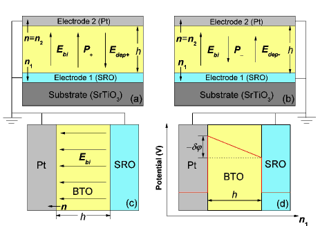
We concentrate on a short-circuited (001) single-domain FE plate of thickness sandwiched between different electrodes. The FE films are fully strained and grown on thick (001) substrate with the polar axis lying normal to the FE-electrode interfaces. Pertsev ; Gerra0 ; Tagantsev We denote the two interfaces as 1 and 2, with surface normals and pointing into the electrodes. The configurations are schematically shown in Fig. 1. The exact value and direction of can be determined as Gerra0 ; Tagantsev
| (1) |
where which is the work function steps for FE-electrode interface at zero polarization is simply defined as the potential difference between the FE and the electrode . Gerra0 ; Tagantsev With the help of first-principles calculations, one could easily obtain through the analysis of the electrostatic potential of FTJs where FE films are in the paraelectric (PE) state. Gerra0 ; Tagantsev
Then, the free energy per unit surface of the FE layer is presented as Gerra0 ; Tagantsev
| (2) | |||||
where are Landau coefficients. Liu is the epitaxial strain and are the elastic compliances coefficients. and are the first order and second order coefficients of the surface energy expansion for the two FE-electrode interfaces. Gerra0 ; Tagantsev is the applied electric field along the polar axis. is the depolarizing field which can be determined from the short-circuit condition such that: Gerra0 ; Tagantsev
| (3) |
where is the permittivity of vacuum space, and indicates the background (i.e. without contribution of the spontaneous polarization) dielectric constant. are the effective screening lengths of the two interfaces and are dependent on the polarization direction if the electronic and chemical environments of FE/electrode interfaces are different. Gerra0 ; Tagantsev For the two opposite polarization orientations, the direction dependence of will induce the asymmetry in potential energy and hence will produce the TER effect, besides the depolarizing field effect due to the polarization difference between two opposite orientations. Tsymbal ; KOHLSTEDT ; Zhuravlev However, we ignore such an effect due to the lack of information about the direction dependence of and we mainly focus on the role of the built-in field in this study. Note that and are thickness and polarization independent and is indeed a long-range internal-bias field which has the effect of poling the FE film. Gerra0 ; Tagantsev ; Simmons In asymmetric FTJs, such asymmetry parameters and can introduce a potential energy profile difference and therefore induce the TER effect. Tsymbal ; KOHLSTEDT ; Zhuravlev
The equilibrium polarization can be derived from the condition of thermodynamic equilibrium:
| (4) |
The dielectric constant under an applied field whose direction is along the polar axis can be determined as: Zheng1
| (5) |
The multiscale thermodynamic model used in this study combines first-principles calculations and phenomenological theory and its detailed description can be found elsewhere. Gerra0 ; Tagantsev In the previous study, it is reported that could result in a smearing of the phase transition and an internal-bias-induced piezoelectric response above in asymmetric FTJs. Gerra0 However, adding to the forgoing controversy on the size effects, further analysis of the effect of built-in field on the FE transition in asymmetric FTJs is still absent. Inserting Eq. (1) into Eq. (2) results in a term that encompasses an odd power of the polarization: , which leads to asymmetric thermodynamic potentials. We shall show that this term which behaves mathematically as identically as the phenomenological term suggested by Bratkovsky and Levanyuk Bratkovsky will result in an unusual FE-“polar non-FE”phase transition in asymmetric FTJs.
III RESULTS AND DISCUSSION
III.1 Size effects
For a quantitative analysis, we consider a fully strained BTO film sandwiched between Pt (electrode 2) and SRO (electrode 1) epitaxially grown on (001) SrTiO3 substrates. We neglect the energy difference of the asymmetric surfaces, i.e. by setting , , to insure that the effect of is clearly observable from the calculations since it is reported that surface effects are generally much smaller than that of . Zheng0 ; Zheng1 All the parameters we used are listed in Ref. 65. We first examine the effect of on the ferroelectricity of asymmetric FTJs. Previous studies indicate that the direction of in asymmetric Pt/BTO/SRO FTJs points to Pt electrode with higher work function. Zheng0 ; Zheng1 ; Cai0 All recent results show indeed that a strong preference for one polarization state namely while disappears at “”. Zheng0 ; Zheng1 ; Cai0 ; Cai1 ; UMENO ; LIU ; LU According to the definition of ferroelectricity, the spontaneous polarization of the FE materials is switchable under an ac electric field. Scott However, knowing that the spontaneous polarization of FE materials is switchable under an ac electric field, Scott recent reports Zheng0 ; Zheng1 ; Cai0 ; Cai1 are rather confusing and remain incomplete on this point. Indeed, in addition to the forementioned divergence in the size effects, two different transition temperatures at which the two polarization states reach zero are obtained (see Ref. 37), which may be confusing since there should be only one finite phase transition temperature for disappearance of ferroelectricity. In order to avoid such confusions, we used the classical definition of ferroelectricicity Scott in the following parts.
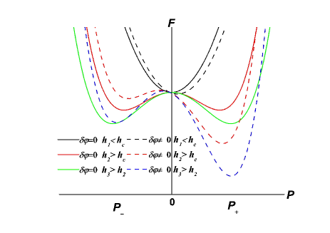
We make further analysis of the physical formulation of in asymmetric FTJs. Note that Eq. (4) is a nonlinear equation and yields “at most”three solutions , two of them corresponding to minima and the other one to a saddle point (unstable state). Whether the solution is a minimum, a maximum or a saddle point can be revealed through inspecting the eigenvalues of the Hessian matrix of the total free energy . Because the asymmetric FTJ is internally biased, i.e., the energy degeneracy between positive and negative is lifted, one of the minima corresponds to the equilibrium state (the global minimum) of the system (the direction of which is along ) and the other minima corresponds to a metastable state (a local minimum) of the system. It means that the presence of two different electrodes in asymmetric FTJs results in a preferred polarization orientation of the FE plate. Having found all solutions as a function of , one can clearly see that metastable state and unstable state solutions become closer to each other and coincide at finite , henceforth the number of solutions drops from three to one. According to the bistable property of FE materials, this finite is just . Scott As long as there are three solutions: two of these three solutions correspond to stable/metastable polarizations so that two orientations of polarization are possible in the BTO layer and thus it is FE. Switching the asymmetric FTJ into its unfavoured high energy polarization may be difficult. If there is the only solution corresponding to the unstable state, although it attains a finite value, it is not FE anymore and may be called “PE”. Indeed it would be more appropriate to consider it as “polar non-FE”since has a unique finite value. Liu1 ; Liu2 ; Okatan FTJs with no built-in field will exhibit two energetically equivalent stable polarization states ( and ) along with an unstable polarization state at below . All the forgoing discussions can be clearly and easily understood in the schematic representation of curves with different BTO thicknesses as shown in Fig. 2 which is quite similar with the results of FE thin films with/without consideration of the fixed interface dipoles near the asymmetric FE/electrode interface UMENO ; LIU ; LU or FE superlattices with/without interfacial space charges. Okatan Together with previous results, LIU ; LU we conclude that no matter the is considered as a long-range field or a short-range surface one, it cannot induce the vanishing of in asymmetric FTJs, which is in contrast with other works. Zheng0 ; Zheng1 ; Cai0 ; Cai1
Note that “polar non-FE”phase is actually a pyroelectric phase because there is a non-switchable polarization in this phase. This kind of phase transition has once been reported in FE thin films with asymmetric electrodes Gerra0 ; UMENO ; LIU ; LU or FE superlattices with interfacial space charge. Liu1 ; Liu2 ; Okatan As we discussed in the formation of , “polar non-FE”phase indeed always corresponds to the unstable state (see Fig. 2) and this kind of non-switchable polarization may not be stable at all. However, breaking up the system into 1800 domain stripes is unambiguously ruled out due to the long-range pinned field . In plane vortex formation NAUMOV1 ; NAUMOV2 is also inhibited because the large compressive strain favors more 1800 domain stripes. NAUMOV2 The ferromagneticlike closure domains are predicted to form in ultrathin FE films or FE capacitors even below Kornev ; PUENTE ; Shimada and are experimentally confirmed well above recently. Nelson ; Jia However, typical FE closure domains Kornev ; PUENTE ; Shimada ; Nelson ; Jia are also not expected in “polar non-FE”phase where 1800 domains in the closure domain structure should be suppressed. But local rotations of non-switchable polarization (900) are still likely to occur and result in a closure-like domain structure since the local change of the direction of the non-switchable polarization especially near the FE/electrode interface is helpful to minimize the system energy. Kornev ; PUENTE ; Shimada Although such closure-like domains can be favored below (3 nm at least), it is clear that the FE barrier as a whole is not FE according to our forgoing analysis that shows the polarization is not switchable under external electric fields. While a detailed analysis of the built-in field effect on domain formation is beyond the scope of this study, we suggest that more rigorous simulations should be made in the future. It can be seen that the asymmetric FTJs below cannot be used for FE memory applications in which two thermodynamic stable polarization states are needed to encode “0”and “1”in Boolean algebra. Mehta ; Junquera ; Kim ; Pertsev ; Gerra0 ; Tagantsev ; Scott However based on our calculation, one should expect a resistance change below between the non-switchable polarization state and the other one being ferroelectrically dead. This result agrees well with recent works on Pt/BTO/Pt FTJs that even below , the resistance of the FTJ would change by a factor of three due to the interface bonding and barrier decay rate effects. VELEV We argue that the TER effect below suggested in our work may be essentially attributed to the asymmetric modification of the potential barrier by the nonzero barrier height () (see Eqs. (1)-(4)) which even exists at zero polarization as shown in Fig. 1(d). Further theoretical and experimental efforts should be made to confirm these predictions.
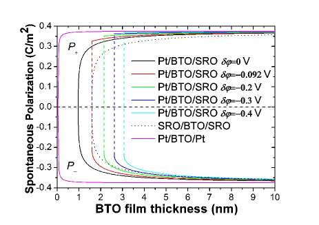
The quantitative results of the forgoing analysis are directly given in Fig. 3. It can be seen that exists regardless of symmetric or asymmetric structures. As expected, the curves of and are symmetric with respect to at where is about 1 nm which is smaller than that of SRO/BTO/SRO, i.e. 1.6 nm. Liu ; Stengel When , the supposed degeneracy between and occurs, i.e. is enhanced while is reduced so the coordinate of the center of the hysteresis loop along the polarization axis [1/2(+ )] is shifted along the direction of . It is shown that such a displacement of the hysteresis loop along the polarization axis becomes more significant as the strength of increases. It may be attributed to the imprint caused by such that the whole shape of the hysteresis loop will shift along the direction of the field axis which is antiparallel to the direction of . Scott Besides, it is found that as increases, increases, which indicates that can enhance the size of . Thus, whether of Pt/BTO/SRO junction is larger or smaller than that in the SRO/BTO/SRO counterpart strongly depends on exact value of as shown in Fig. 3.
For the symmetric structures (SRO/BTO/SRO and Pt/BTO/Pt FTJs), one can easily see in Fig. 3 that single domain in the FE layer destabilizes as the film thickness is decreased due to the depolarizing field effect. Liu ; Mehta ; Junquera ; Kim ; Pertsev ; Gerra0 ; Tagantsev And it is shown in Fig. 3 that Pt/BTO/Pt FTJ whose is merely 0.08 BTO unit cell is nearly free of deleterious size effects, Liu which agrees well with the result of first-principles calculations. Stengel of SRO/BTO/SRO FTJ is about four BTO unit cells, which is consistent well with our previous results. Liu The qualitative result that of Pt/BTO/Pt FTJ is smaller than that of SRO/BTO/SRO FTJ in this work is consistent well with those of first-principles calculations Stengel and lattice model. Wang However, our results are in contrast with previous works Kim ; Zheng0 ; Zheng1 predicting of SRO/BTO/SRO FTJ to be smaller than that of Pt/BTO/Pt FTJ. In these previous works, Zheng0 ; Zheng1 Mehta et al’ electrostatic theory about the depolarizing field ( where and are Thomas-Fermi screening lengths and and are dielectric constants of electrode 1 and 2) is used Mehta while in our work we used the “effective screening length”model to describe the depolarizing field (see Eq. (3)). Note that we used the same parameters as Refs. 36 and 37 except for the model of depolarizing field. parameters The distinct results are understandable since it is generally accepted that imperfect screening should be characterized by effective screening length (See Eq. (3)) rather than Thomas-Fermi one in Mehta et al’ model. Junquera1 In fact, the effective screening length at Pt/BTO interface is only 0.03 Å Stengel much smaller than that of Thomas-Fermi one 0.4 Å, Kim so a significantly reduced depolarizing field is expected and it would result in nearly no in Pt/BTO/Pt FTJs. Previous study attributes this freedom of size effects in the Pt/BTO/Pt structure to the “negative dead layer”near the Pt/BTO interface, Stengel while we argue that it may result directly from the fact that the effective screening length of Pt electrode is extremely small since Bratkovsky and Levanyuk suggested the “dead layer”model is totally equivalent as to consider an electrode with a finite screening length. Bratkovsky1 Here we ignore the effect of the extrinsic “dead layer”formed between metal electrode (i.e. Au or Pt) and a perovskite FE (i.e. Pb(ZrTi)O3 or BTO). Indeed, Lou and Wang found that the “dead layer”between Pt and Pb(ZrTi)O3 is extrinsic and could be removed almost completely by doping 2% Mn. Lou Experimentally, many researchers found that SRO/BTO/SRO capacitors (as well as other perovskite FE structures with conductive oxide electrodes) are free from passive layers. Kim ; Kim1 ; Jin Recently, a very interesting experimental result demonstrates that the RuO2/BaO terminations at BTO/SRO interface, which is assumed as many pinned interface dipoles and plays a detrimental role in stabilizing a switchable FE polarization, can be overcome by depositing a very thin layer of SrTiO3 between BTO layer and SRO electrode. LIU ; LU Nonetheless, it is still unclear whether such pinned interface dipoles are intrinsic and can be found in other FE/electrode interfaces (i.e. SRO/PbTiO3 and Pt/BTO).
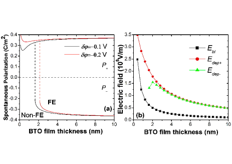
In the asymmetric structures in Fig. 3, it is shown that in comparison with in asymmetric Pt/BTO/SRO FTJs, is significantly enhanced, as increases, which is in good agreement with the recent results regarding as short-range interface field, LIU and is similar with the previous results. Zheng1 Note that is intrinsic and determined strictly by the electronic and chemical environments of FE/electrode interfaces but not by any potential drop through the FTJ which “creates”an applied field. Gerra0 ; Tagantsev ; Bratkovsky ; Simmons Changing is simply due to the lack of its exact value and for the purpose of studying the effect of in asymmetric FTJs, which is similar to the previous method. Zheng0 ; Zheng1 This method Zheng0 ; Zheng1 indeed does not mean that any asymmetric electrodes are considered here, since the electrode is replaced, the electrode/FE interface parameters in Eqs. (1)-(3) such as and other interface parameters will also change. The variation of in Pt/BTO/SRO FTJs as a function of the whole BTO layer thickness with =-0.1 V and -0.2 V at 0 K is shown in Fig. 4(a). It is found that below the critical thickness state shows an interesting recovery of a polar non-FE polarization, in contrast to state (see Fig. 4(a)), becoming less significant when -0.2 V. Note that such recovery has been reported in FE superlattices with asymmetric electrodes and demonstrated to be independent of the interfacial space charge. Liu1 Although such a recovery of polar non-FE polarization in BTO layer does not mean the recovery of ferroelectricity as it is not switchable, it is necessary to realize its origin. We plot the build-in field and depolarizing field for different directions, and , as a function of the BTO film thickness considering =-0.1 V as an example in Fig. 4(b). For the condition of state as schematically illustrated in Fig. 1(b), shows the typical behavior as the FTJ with the same electrodes, Junquera ; Kim ; Pertsev ; Wang which means that plays a key role forcing the single domain in the FE layer to destabilize as the film thickness is decreased. with the same direction of helps then to speed up such destabilization, therefore enhancing the critical thickness. For the state, and are in the opposite directions, as depicted in Fig. 1(a), and both the strengths of and increase as the BTO layer thickness is decreased (Fig. 4(b)), which means that is partially cancelled by . The strength of this partial compensation becomes stronger with the film thickness decreasing (see the slopes of and curves)(Fig. 4(b)). Therefore, is fighting against allowing the polarization to recover into a polar non-FE polarization. This recovery of polar non-FE polarization forces the system to a higher energy state which strongly supports our forgoing predictions of local rotations of non-switchable polarization (900) and the formation of closure-like domain structure to minimize the system energy.
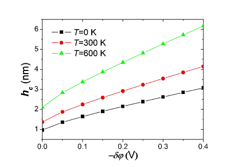
The critical thickness under different ambient temperatures as a function of () in asymmetric Pt/BTO/SRO FTJs is shown in Fig. 5. It can be seen that decreases with increasing. And it is found that for other , the asymmetric Pt/BTO/SRO FTJs show a similar behavior of enhancement of by increasing the strength of as shown in Fig. 3 at 0 K.
III.2 Transition temperature and dielectric response
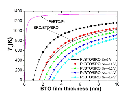
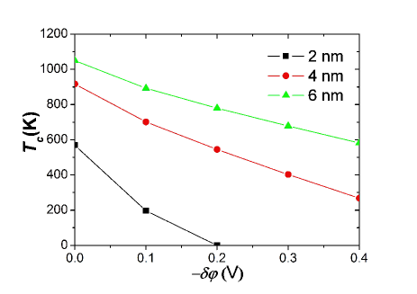
The transition temperature of the asymmetric FTJs is extremely important, especially for the device applications. Fig. 6 summarizes as a function of BTO thickness in epitaxial asymmetric Pt/BTO/SRO FTJs at various values of . It is shown that in asymmetric Pt/BTO/SRO FTJs monotonically decreases with the BTO layer thickness decreasing, which is similar to the behavior of symmetric SRO/BTO/SRO or Pt/BTO/Pt FTJs. Liu Moreover, decreases more significantly for thinner BTO barrier layer thickness (see the slope of curves in Fig. 6). At a given BTO layer thickness, it is found in Fig. 7 that decreases as becomes more negative, which means a larger built-in field can force the phase transition to occur at lower temperatures. The transition temperature is strongly sensitive to the change especially for the thinner BTO barrier (see the slope of curves in Fig. 7). It can be clearly seen that the FE transition temperature is suppressed as the built-in field is increased for different BTO thicknesses. Usually, the TER effect is always significantly larger for thicker barrier with larger polarization. Garcia0 ; Zhuravlev Here we find that a fundamental limit (which is more drastic for thinner FE barrier thickness) on the work temperature of FTJ-type or capacitor-type devices should also be simultaneously taken into account together with the FE barrier thickness or polarization value. In addition and interestingly, since the electrocaloric effect is always the strongest close to the FE-PE transition, Scott2 such tuning of by should be also considered in potential asymmetric FTJs for the room temperature solid-state refrigeration. Liu Moreover, the fact that large tunneling current in asymmetric FTJs Gruverman results in significant Joule heating should also be included in the design of future devices.
| (V) | (K) | |||
|---|---|---|---|---|
| 0 | 1086 | 1001.4 | 24.8 | 513.1 |
| -0.1 | 1223 | 428.5 | 23.0 | 225.7 |
| -0.2 | 1345 | 285.8 | 21.4 | 153.6 |
| -0.3 | 1465 | 218.3 | 20.1 | 119.2 |
| -0.4 | 1574 | 178.1 | 18.9 | 98.5 |
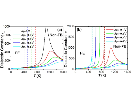
The dielectric response ( is parallel to ) and ( is antiparallel to ) of Pt/BTO/SRO FTJs (consider the 5-nm-thick BTO film as an example) as a function of at different is shown in Figs. 8(a) and (b). Several key parameters with different in Fig. 8(a) are extracted in Table. 1: corresponds to the temperature where reaches its maximum, ; simply means the minimal value of ; is in somehow the diffuseness of the transition. It can be seen that when , shows a sharp peak near . However, a gradual decrease in and is seen upon increasing which is well consistent with the results of smearing of by increasing in Fig. 6 (see the slope of curves in Fig. 6). The diffusive transition response in clearly shows smearing of the phase transition as a result of , which verifies the predictions of Tagantsev et al Gerra0 ; Tagantsev and Bratkovsky et al. Bratkovsky In addition, it is shown is shifted to higher temperatures due to . As the strength of increases, the smearing of phase transition and the shift of becomes more significant. On the other hand, the applied field cannot fully compensate the built-in field, resulting in a discountinuous phase transition from FE phase to polar non-FE phase with temperature increasing as depicted in dielectric response in Fig. 8(b), which is distinct from the countinuous counterpart of as shown in Fig. 8(a). abruptly changes its sign near the transition point resulting a dielectric peak and a similiar smearing of by increasing the strength of is found. Furthermore, it is found that though the transition temperatures for two directions are different, they both decrease as the built-in field increases which is consistent with the results without any external field (See Fig. 6), which indicates that the built-in field forces the transition to take place at a reduced temperature.
III.3 Comments on the built-in field effect
We make further comments on the built-in field effect in asymmetric FTJs. The main assumption in this study is that does not change during the polarization reversal. Gerra0 ; Tagantsev The presence of which results in an asymmetric potential energy and barrier height differences by switching the polarization will induce the TER effect. Tsymbal ; KOHLSTEDT ; Zhuravlev Note that the switching of the polarization in the asymmetric FTJs may change the value of . VELEV ; VELEV1 ; UMENO ; Stengel2 ; Chen However, according to our analysis, the variation in (even changing its sign occurs during the polarization reversal) does not alter the main results of this study due to its induced broken spatial inversion symmetry of FTJs. In addition to the built-in field, if the surface term is nonzero, the main conclusions of this paper will not change as well.
IV CONCLUSIONS
In summary, on the basis of a multiscale thermodynamic model, a detailed analysis of the changes brought by the built-in electric field in asymmetric FTJs is made. It is demonstrated that the critical thickness does exist in asymmetric FTJs. Below the critical thickness, it is found that there is a recovery of polar non-FE polarization due to strong cancelling of the depolarizing field by the built-in field, and closure-like domains are proposed to form to minimize the system energy. It is found that the built-in electric field could not only induce imprint and a behavior of smearing of the FE phase transition but also forces the phase transition to take place at a reduced temperature. A fundamental limit of transition temperature dependence of the barrier layer thickness on the work temperature of FTJ-type or FE capacitor-type devices is proposed and should be simultaneously taken into account in the further experiments. Hopefully, our results will be helpful to the fundamental understandings of phase transitions in asymmetric FTJs.
Acknowledgements.
This work is supported by the Ministry of Science and Technology of China through a 973-Project under Grant No. 2012CB619401. The authors gratefully thank Dr. X. Y. Wang, Dr. M. B. Okatan, and Prof. S. P. Alpay for their fruitful suggestions. Y. Liu is thankful to the Multidisciplinary Materials Research Center (MMRC) at Xi’an Jiaotong University for hospitality during his visit. Y. Liu and B. Dkhil wish to thank the China Scholarship Council (CSC) for funding YL’s stay in France. Y. Liu, M. Bibes and B. Dkhil also acknowledge the Agence Nationale pour la Recherche for financial support through NOMILOPS (ANR-11-BS10-016-02) project. X. J. Lou would like to thank the “One Thousand Youth Talents”program for support.References
- (1) E. Y. Tsymbal, A. Gruverman, V. Garcia, M. Bibes, and A. Barthélémy, MRS Bulletin 37, 138 (2012).
- (2) H. Kohlstedt, N. A. Pertsev, J. Rodíguez Contreras, and R. Waser, Phys. Rev. B 72, 125341 (2005).
- (3) M. Y. Zhuravlev, R. F. Sabirianov, S. S. Jaswal, and E. Y. Tsymbal, Phys. Rev. Lett. 94, 246802 (2005).
- (4) J. P. Velev, C.-G. Duan, K. D. Belashchenko, S. S. Jaswal, and E. Y. Tsymbal, Phys. Rev. Lett. 98, 137201 (2007).
- (5) V. Garcia, S. Fusil, K. Bouzehouane, S. Enouz-Vedrenne, N. D. Mathur, A. Barthélémy, and M. Bibes, Nature (London) 460, 81 (2009).
- (6) A. Gruverman, D. Wu, H. Lu, Y. Wang, H. W. Jang, C. M. Folkman, M. Y. Zhuravlev, D. Felker, M. Rzchowski, C. B. Eom, and E. Y. Tsymbal, Nano Lett. 9, 3539 (2009).
- (7) A. Crassous, V. Garcia, K. Bouzehouane, S. Fusil, A. H. G. Vlooswijk, G. Rispens, B. Noheda, M. Bibes, and A. Barthélémy, Appl. Phys. Lett. 96, 042901 (2010).
- (8) A. Chanthbouala, A. Crassous, V. Garcia, K. Bouzehouane, S. Fusil, X. Moya, J. Allibe, B. Dlubak, J. Grollier, S. Xavier, C. Deranlot, A. Moshar, R. Proksch, N. D. Mathur, M. Bibes, and A. Barthélémy, Nat. Nanotechnol. 7, 101 (2011).
- (9) D. I. Bilc, F. D. Novaes, J. Íñiguez, P. Ordejón, and P. Ghosez, ACS Nano 6(2), 1473 (2012).
- (10) D. Pantel, H. D. Lu, S. Goetze, P. Werner, D. J. Kim, A. Gruverman, D. Hesse, and M. Alexe, Appl. Phys. Lett. 100, 232902 (2012).
- (11) A. Chanthbouala, V. Garcia, R. O. Cherifi, K. Bouzehouane, S. Fusil, X. Moya, S. Xavier, H. Yamada, C. Deranlot, N. D. Mathur, M. Bibes, A. Barthélémy, and J. Grollier, Nat. Mater. 11, 860 (2012).
- (12) M. Y. Zhuravlev, S. S. Jaswal, E. Y. Tsymbal, and R. F. Sabirianov, Appl. Phys. Lett. 87, 222114 (2005).
- (13) C.-G. Duan, S. S. Jaswal, and E. Y. Tsymbal, Phys. Rev. Lett. 97, 047201 (2006).
- (14) S. Sahoo, S. Polisetty, C.-G. Duan, S. S. Jaswal, E. Y. Tsymbal, and C. Binek, Phys. Rev. B 76, 092108 (2007).
- (15) C.-G. Duan, Julian P. Velev, R. F. Sabirianov, W. N. Mei, S. S. Jaswal, and E. Y. Tsymbal, Appl. Phys. Lett. 92, 122905 (2008).
- (16) M. K. Niranjan, J. D. Burton, J. P. Velev, S. S. Jaswal, and E. Y. Tsymbal, Appl. Phys. Lett. 95, 052501 (2009).
- (17) J. D. Burton and E. Y. Tsymbal, Phys. Rev. B 80, 174406 (2009).
- (18) J. P. Velev, C.-G. Duan, J. D. Burton, A. Smogunov, M. K. Niranjan, E. Tosatti, S. S. Jaswal, and E. Y. Tsymbal, Nano Lett. 9, 427 (2009).
- (19) M. Y. Zhuravlev, S. Maekawa, and E. Y. Tsymbal, Phys. Rev. B 81, 104419 (2010).
- (20) V. Garcia, M. Bibes, L. Bocher, S. Valencia, F. Kronast, A. Crassous, X. Moya, S. Enouz-Vedrenne, A. Gloter, D. Imhoff, C. Deranlot, N. D. Mathur, S. Fusil, K. Bouzehouane, and A. Barthélémy, Science 327, 1106 (2010).
- (21) M. Hambe, A. Petraru, N. A. Pertsev, P. Munroe, V. Nagarajan, and H. Kohlstedt, Adv. Funct. Mater. 20, 2436 (2010).
- (22) S. Valencia, A. Crassous, L. Bocher, V. Garcia, X. Moya, R. O. Cherifi, C. Deranlot, K. Bouzehouane, S. Fusil, A. Zobelli, A. Gloter, N. D. Mathur, A. Gaupp, R. Abrudan, F. Radu, A. Barthélémy, and M. Bibes, Nat. Mater. 10, 753 (2011).
- (23) H. L. Meyerheim, F. Klimenta, A. Ernst, K. Mohseni, S. Ostanin, M. Fechner, S. Parihar, I. V. Maznichenko, I. Mertig, and J. Kirschner, Phys. Rev. Lett. 106, 087203 (2011).
- (24) L. Bocher, A. Gloter, A. Crassous, V. Garcia, K. March, A. Zobelli, S. Valencia, S. Enouz-Vedrenne, X. Moya, N. D. Marthur, C. Deranlot, S. Fusil, K. Bouzehouane, M. Bibes, A. Barthélémy, C. Colliex, and O. Stáphan, Nano Lett. 12, 376 (2012).
- (25) J. M. López-Encarnación, J. D. Burton, Evgeny Y. Tsymbal, and J. P. Velev, Nano Lett. 11, 599 (2011).
- (26) D. Pantel, S. Goetze, D. Hesse, and M. Alexe, Nat. Mater. 11, 289 (2012).
- (27) Y. Liu, X.-P. Peng, X. J. Lou, and H. Zhou, Appl. Phys. Lett. 100, 192902 (2012).
- (28) X. Luo, B. Wang, and Y Zheng, ACS Nano 5(3), 1649 (2011); H. Lu, D. J. Kim, C.-W. Bark, S. Ryu, C. B. Eom. E. Y. Tsymbal, and A. Gruverman, Nano Lett. 12, 6289 (2012).
- (29) R. R. Mehta, B. D. Silverman, and J. T. Jacobs, J. Appl. Phys. 44, 3379 (1973).
- (30) J. Junquera and P. Ghosez, Nature (London) 422, 506 (2003).
- (31) D. J. Kim, J. Y. Jo, Y. S. Kim, Y. J. Chang, J. S. Lee, J.-G. Yoon, T. K. Song, and T. W. Noh, Phys. Rev. Lett. 95, 237602 (2005).
- (32) N. A. Pertsev and H. Kohlstedt, Phys. Rev. Lett. 98, 257603 (2007).
- (33) G. Gerra, A. K. Tagantsev, and N. Setter, Phys. Rev. Lett. 98, 207601 (2007).
- (34) A. K. Tagantsev, G. Gerra, and N. Setter, Phys. Rev. B 77, 174111 (2008).
- (35) M. Stengel, D. Vanderbilt, and N. A. Spaldin, Nature Mater. 8, 392 (2009).
- (36) Y. Zheng, W. J. Chen, C. H. Woo, and B. Wang, J. Phys. D: Appl. Phys. 44, 139501 (2011).
- (37) Y. Zheng, W. J. Chen, X. Luo, B. Wang, and C. H. Woo, Acta Materialia 44, 139501 (2012).
- (38) M.-Q. Cai, Y. Zheng, P.-W. Ma, and C. H. Woo, J. Appl. Phys. 109, 024103 (2011).
- (39) M.-Q. Cai, Y. Du, and B.-Y. Huang, Appl. Phys. Lett. 98, 102907 (2011).
- (40) Y. Umeno, J. M. Albina, B. Meyer, and C. Elsässer, Phys. Rev. B 80, 205122 (2009).
- (41) X. H. Liu, Y. Wang, P. V. Lukashev, J. D. Burton, and E. Y. Tsymbal, Phys. Rev. B 85, 125407 (2012).
- (42) H. Lu, X. Liu, J. D. Burton, C.-W. Bark, Y. Wang, Y. Zhang, D. J. Kim, A. Stamm, P. Lukashev, D. A. Felker, C. M. Folkman, P. Gao, M. S. Rzchowski, X. Q. Pan, C.-B. Eom, E. Y. Tsymbal, and A. Gruverman, Adv. Mater. 24, 1209 (2012).
- (43) J. G. Simmons, Phys. Rev. Lett. 10, 10 (1963).
- (44) A. M. Bratkovsky and A. P. Levanyuk, Phys. Rev. Lett. 94, 107601 (2005).
- (45) J. F. Scott, Ferroelectric Memories (Springer, Berlin, 2000).
- (46) Y. Liu and X.-P. Peng, Applied Physics Express 5, 011501 (2012).
- (47) Y. Liu and X.-P. Peng, Chinese Physics Letters 29, 057701 (2012).
- (48) M. B. Okatan, I. B. Misirlioglu, and S. P. Alpay, Phys. Rev. B 82, 094115 (2010).
- (49) J. Junquera and P. Ghosez, J. Comput. Theor. Nanosci. 5, 2071 (2008).
- (50) I. I. Naumov, L. Bellaiche, and H. X. Fu, Nature (London) 432, 737 (2004).
- (51) I. Naumov and A. M. Bratkovsky, Phys. Rev. Lett. 101, 107601 (2008).
- (52) I. Kornev, H. X. Fu, and L. Bellaiche, Phys. Rev. Lett. 93, 196104 (2004).
- (53) P. Aguado-Puente and J. Junquera, Phys. Rev. Lett. 100, 177601 (2008).
- (54) T. Shimada, S. Tomoda, and T. Kitamura, Phys. Rev. B 81, 144116 (2010).
- (55) C. T. Nelson, B. Winchester, Y. Zhang, S.-J. Kim, A. Melville, C. Adamo, C. M. Folkman, S.-H. Baek, C.-B. Eom, D. G. Schlom, L.-Q. Chen, and X. Q. Pan, Nano Lett. 11, 828 (2011).
- (56) C.-L. Jia, K. W. Urban, M. Alexe, D. Hesse, and I. Vrejoiu, Science 331, 1420 (2011).
- (57) X. Y. Wang, Y. L. Wang, and R. J. Yang, Appl. Phys. Lett. 95, 142910 (2009); Y. L. Wang, X. Y. Wang, Y. Liu, B. T. Liu, and G. S. Fu, Physics Letters A, 374, 4915 (2010).
- (58) A. M. Bratkovsky and A. P. Levanyuk, J. Comp. Theor. Nanosci. 6, 465 (2005).
- (59) X. J. Lou and J. Wang, Journal of Physics: Condensed Matter 22, 055901 (2010).
- (60) Y. S. Kim, J. Y. Jo, D. J. Kim, Y. J. Chang, J. H. Lee, T. W. Noh, T. K. Songa, J.-G. Yoon, J.-S. Chung, S. I. Baik, Y.-W. Kim, and C. U. Jung, Appl. Phys. Lett. 88, 072909 (2006).
- (61) H. Z. Jin and J. Zhu, J. Appl. Phys. 92, 4594 (2002).
- (62) J. F. Scott, Annu. Rev. Mater. Res. 41, 229 (2011).
- (63) M. Stengel, P. Aguado-Puente, N. A. Spaldin, and J. Junquera, Phys. Rev. B 83, 235112 (2011).
- (64) F. Chen and A. Klein, Phys. Rev. B 86, 094105 (2012).
- (65) We used the following set of parameters (in SI units): , , , , , , , , . Landau coefficients (the expressions can be origianlly found in N. A. Pertsev, A. K. Tagantsev, and N. Setter, Phys. Rev. B 61, R825 (2000)), electrostrictive coefficients, and elastic compliances of BTO at room temperature we used are the same as those in Refs. 27, 36 and 37. The effective screening length and the coefficients of the surface energy expansion are taken from Refs. 33, 34 and 35, respecticely. The background dielectric constant is taken from Refs. 36 and 37 which is distinct from 7 used in Refs. 33 and 34. In fact, there is no consensus on its exact value, especially by the theoretical researchers. In this study, we have made some comparisons with the previous studies in Refs. 36 and 37, so selecting 50 is reasonable and does not change the main results of this work. The approximated parameters in this work need more rigorous treatment by the first-principles calculations or experimental confirmation in the future.