Thin films thickness Measurement by the conductivity theory in the framework of born approximation
Abstract
When the thickness of the layer is smaller than the electrons mean free path, the morphology affects the conductivity directly based on the layer thickness. This issue provides basis in order to estimate the thickness of the layer by understanding the morphology and the value of the conductivity. This method is an inverse approach on thickness estimation and is applied to various samples. The comparison of the results with other thickness estimations shows good consistency. The benefits of this approach is that the only parameter that needs to be measured is the conductivity, which is quite trivial. Despite the simplicity of this approach, its results would prove adequate to study both the material properties and the morphology of the layer. In addition, the possibility of repeating the measurements on thickness for AC currents with various frequencies enables averaging the measurements in order to obtain the most precise results.
keywords:
Electrical conductivity , Ultra thin film Rough surfaces1 Introduction
A wide range of studies have been carried out on the conductivity properties of thin films in the past. A very popular aspect of studying electric conductivity of thin films is its dependence on the surface Thompson (1990). The first classical formulation in this context was proposed by Fuchs (1990) and generalized considering the presence of a magnetic field by Sondheimer et al. (1949). The logic behind considering the magnetic field Kao (1965) is that the thickness of the thin film (e.g. Indium) would affect the critical magnetic field, consequently affecting the transition from the super-conducting state to the normal state Toxen (1961). A lot of effort has been invested on surfaces in the presence of magnetic fields in the context of e.g. surface quantum states and impedance oscillations Nee et al. (1968); Khaikin (1969), electron scattering Koch (1969); Cheng (1973) and transport (conductivity) Gold (1987); Fishman et al. (1989); Palasantzas et al. (1997); Palasantzas (2005); Meyeroyich et al. (1999), etc, which where all based on the quantum mechanical formulation Prange et al. (1968). Quantum size effects and surface roughness influences the conductivity of ultra-thin magnetic layers Barnas et al. (1995, 1995); Jalochowski et al. (1992, 1996) and wave scattering Zamani et al. (2012); Jafari et al. (2005).
A general expression was suggested for the dependence of the conductivity on the thin film thickness Fishman et al. (1989), where the surface roughness was characterized by the autocorrelation function that described all the electrical properties of the system. This enabled discussion on the interplay of the correlation length of the surface and the Fermi wave vector with regards to the conductivity Fishman et al. (1991). Note that in this model the thin films thicknesses is smaller than the bulk electrons’ mean free path. It was deduced that the conductivity only depends on the thickness of the film provided that , where and are the correlation length of the surface and the Fermi wave vector, respectively. But on the other hand, for the case , the autocorrelation function would act effectively on the conductivity of the thin film Fishman et al. (1989, 1991).
In a series of studies, Palasantzas extended the previous models by pointing out that the film surface ought to be considered fractal. In a sense that the local fractal dimensions would also affect the characteristics of the self-affine fractal model (e.g. electric conductivity) for one rough layer Palasantzas et al. (1997) or two rough layers Palasantzas et al. (2000). Here we take an inverse approach based on the two layer self-affine fractal model of Palasantzas Palasantzas et al. (2000), where we measure the electric conductivity in order to obtain details on the thickness of the layer. In this article we implement a model to determine the thickness of metallic films with two rough boundaries that is based on their conductivity in the framework of Born approximation. In section II, the theory and formulation for the conductivity based on Born approximation in presence of two rough boundaries is illustrated. In section III, effects of conductivity on the thickness of the layer is discussed in addition to the by product effects of the alternate and direct currents applied to the layer its resistance. In section IV the summary is stated.
2 Inverse method for measuring the thin-films thickness
Consider a thin film of two rough surfaces with thickness , which its thickness is smaller than the mean free path of the electron. The thin film crosses the z-axis at and , with and , where and are the random roughness fluctuations of surface and respectively with Palasantzas et al. (2000). Note that the choice of the quantum mechanical formulation in this limitation is due to the fact that the thickness layer is smaller than the mean free path of the electron. In this case the electrons would scatter from the surface before being scattered by the bulk electrons Palasantzas et al. (1997, 2000). The conductivity relation for the case where the surface roughness is considered much smaller than the film thickness ) is Palasantzas et al. (2000)
| (1) |
where is the number of occupied mini-bands, is the Fermi energy, is the scattering matrix which contains two terms: incoherent term , (incoherent scattering by two rough interfaces) and cross-correlation term , (coherent scattering by two interfaces). The elements of and describe intra- and inter-subband transitions, which is expressed by Palasantzas et al. (2000)
| (2) |
and
| (3) |
In Eq. (2), is the Fourier transform of the auto-correlation function expressed as . In Eq. (3) is the Fourier transform of the cross correlation function with . The wave vectors of and miniband edges in Eqs (2) and (3) are expressed as and , with being the angle between and . In the case where the potential tends to infinity, the parameters and are defined as and and respectively, for details of the model see Palasantzas et al. (2000).
Consider a fractal surface Barabasi et al. (1995); Ebrahiminejad et al. (2012); Zamani et al. (2012) with roughness , correlation length , and roughness exponent . In order to obtain the conductivity (Eq. (1)) of the system, it is essential to have the power spectrum for each surface in addition to the power spectrum for their cross correlation Palasantzas et al. (1997); Zhao et al. (2001)
| (6) | |||
| (9) |
It is worth mentioning that the power spectrum defined by Eq. (6) only works for fractal surfaces Zhao et al. (2001).
The aim of this work is to estimate the thickness by the measured conductivity making use of Eq. (1). This is an inverse method to previous methods where the conductivity was obtained by the measured thickness of the layer, see Palasantzas et al. (1997, 2000). Due to the fact that for any typical rough surface where the roughness is of the same order as the thickness, the surface parameters (e.g. surface roughness) would be effective on the determination of the layers thickness. Note that distinguishing the roughness of the surface from the thickness of the layer is not a simple task, this complicates the correct estimation of the thickness. Hence, experimental measurements of the conductivity would be more trivial compared to measuring the thickness.
The inverse method illustrated in this work is based on the following procedure;
- The AFM images of the interface between the substrate and the layer together with the AFM images of the layer and air needs to be produced in order to find the fluctuations of the surface .
- From the logarithmic plot of the height-height correlation function Zhao et al. (2001) the surface parameters for each interface is obtained.
- Having in hand the surface parameters, the power spectrum could be obtained by Eq. (4). Hence, the scattering matrix of Eqs. (2) and (3) could be obtained. - In the final stage, comparing the experimental measurements for the conductivity with the analytical results obtained from Eq. (1) the thickness is obtained.
3 Discussion and conclusions
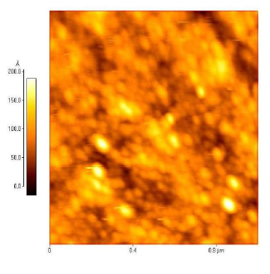
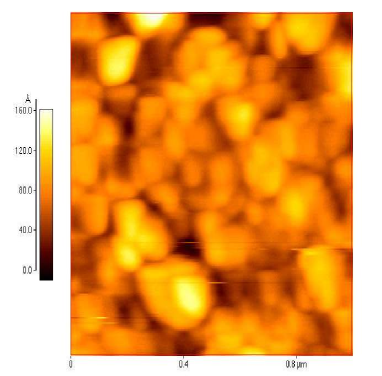
The sample that we considered was a copper thin film that had been coated with a coating rate of , where after seconds, the thickness of was achieved. The topography of the samples were investigated using Atomic force microscopy (AFM) with Park Scientific Instruments (model Autoprobe CP). The images were scanned into pixels in a constant force mode and digitised with the scanning frequency of . The AFM images (Fig. 1) are shown for both the film interface with air and the film interface with the substrate. For this sample the thickness of the thin film is calculated by using Eq. (1).
In order to obtain the surface parameters, the height-height correlation function in addition to the height fluctuations of the surface needs to be obtained. In Fig. 2 the logarithmic height-height correlation function corresponding to the interface between the layer and substrate (bottom curve) and the interfaces between the layer and air (top curve) is plotted making use of equation for .
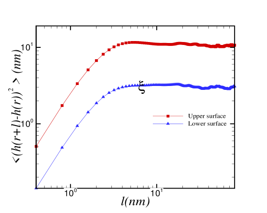
The surface parameters for the copper sample under consideration is extracted from Fig. 2 as
| (10) |
The power spectrums and which could readily be seen in Eq. (2) could be obtained by substituting the parameters of Eq. (3) in Eq. (6). This results in obtaining the incoherent scattering matrix . To calculate the coherent scattering matrix (Eq. (3)) the cross power spectrum needs to be obtained. This obliges us to plot the height-height cross correlation function which shows to be approximately just a straight line.
Having the values for and , the conductivity (Eq. (1)) could be plotted as a function of thickness, see Fig. 3. For the copper sample under study, the measured conductivity was reported as , thus according to Fig. 3, the thickness could be estimated about which is in good agreement with values obtained by direct experimental measurements for conductivity.
Since, for our sample is of the order of , and the average power spectrum of each rough boundary is of the order of , the scattering due to the cross-correlation of the two interfaces is smaller than the scattering due to each of the rough surfaces. This issue motivates finding the effect of the cross-correlation term on conductivity by removing this term from the conductivity equation (Eq. (1)). In Fig. 3 graphs of electrical conductivity of Cu thin film with and without the coherent term is illustrated. It is evident that the cross correlation term causes a small shift in conductivity. It could be understood that the cross correlation effects on conductivity is inversely proportional to the surface thickness. However, this issue could be shown by plotting the relative difference of the conductivity against the thickness, see right panel of Fig. 3.
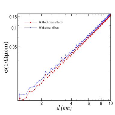
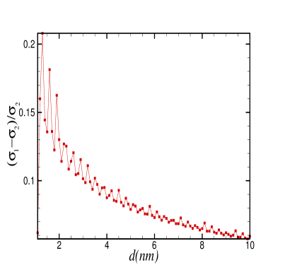
It could be deduced form Fig. 3 that for a layer with thickness , the consideration of the cross correlation effects would cause an increase of about percent in the conductivity. Whereas, for a layer with , this effect would cause an increase of about percent.
It is well known that the accumulation of electrons at sharp points of a surface is more efficient than other places. Based on this concept the height fluctuations of a rough surface would prove adequate for accumulation of charges. This leads to the appearance of local capacities on the rough surface. If a DC current is applied to the surface due to the fact that the frequency is infinity, this issue does not affect the electric conductivity. But if an AC current is applied to the surface, additional resistance is seen in the system. This resistance is obtained from , where is the frequency of the incident wave and is the capacitance. The capacitance is obtained by Palasantzas (2005)
| (11) |
where is the capacitance of two smooth electrode surfaces . Note that Eq. (11) works for a capacitor with one rough surface. In our case of study the capacitor consists of two rough surfaces, this issue obliges further consideration for obtaining the capacitance. In order to overcome this issue, due to the assumption that the reciprocal correlation is weak, we may consider the system as two capacitors in series. Where each capacitor has one rough surface. This enables (having in hand the morphology parameters of the surface) measuring the capacitance effects of the thin Cu layer under an AC current. Equation (11) would give the capacitance for the Cu sample by knowing the roughness parameters. Consequently the capacitance resistance could be obtained from the capacitance.
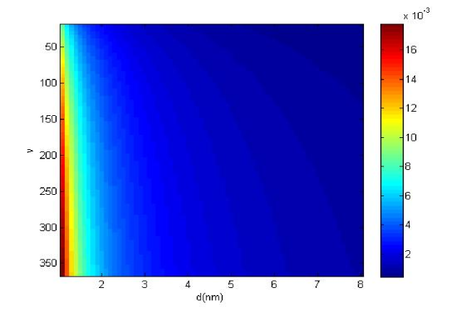
Fig. 4 illustrates dependence of the resistivity of the thin Cu layer on the layer thickness and the frequency of the AC current applied to the layer. It could readily be noticed that for a typical layer with specific morphological parameters, by keeping the frequency constant, the capacitance resistance would be proportional to the thickness of the layer. This could be explained by the fact that capacitance is inversely proportional to the thickness of the layer inside a capacitor. Hence, for thicker layers and lower AC frequencies, in addition to the Ohmic resistivity, capacitance resistivity would also come in to play, this is due to the creation of local capacitors.
4 Summary
- An inverse method was proposed to estimate the thin layer thickness by means of the electric conductivity and the surface morphology parameters of the layer.
- This method enables to obtain an ensemble average over the various measurements of the layer thickness by repeating them for different AC and DC currents. This could reduce the estimation errors of the layer thickness.
- The reciprocal (cross) correlation of the two rough surfaces of the thin films increases or decreases the conductivity depending on its sign (positive sign gives an increase and negative sign gives a decrease) in comparison to the case where the surfaces where considered solitary to each other.
- The efficiency of the reciprocal correlation between two rough surfaces is inversely proportional to the thickness of the layer. This means that as the thickness of the layer increases the effects of the reciprocal correlation on the conductivity of the layer is less efficient.
- An additional resistance to the local resistance of the capacitor due to the alternate current comes in to play. This resistance which is named as the capacitance resistance does not exist for the case of direct current. This is due to the fact that the height fluctuations create local capacitors on the substrate, and as an alternate current passes through it an RC circuit is performed.
Acknowledgments: G.R. Jafari would like to thank the research council of Shahid Beheshti University for financial support. In addition the authors would like to thank Fatemeh Iranmanesh for her helpful comments and Sharmin Kharazi for helping to edit the manuscript.
References
- Thompson (1990) J. Thompson, Proc. Camb. Pholos. Soc. 11, 1120 (1901).
- Fuchs (1990) K. Fuchs, Proc. Philos. 34, 100 (1938).
- Sondheimer et al. (1949) E. H. Sondheimer, Nature 164, 920 (1949).
- Kao (1965) yi-Han Kao, Phys. Rev. 138, 1412 (1965).
- Toxen (1961) A. M. Toxen, Phys. Rev. 123, 442 (1961).
- Nee et al. (1968) T. W. Nee, J. F. Koch, R. E. Prange, Phys. Rev. 174, 758 (1968).
- Khaikin (1969) M. S. Khaikin, Adv. Phys. 18, 1 (1969).
- Koch (1969) J. F. Koch, T. E. Murray, Phys. Rev. 186, 722 (1969).
- Cheng (1973) Y. C. Cheng, E. A. Sullivan, Surf. Sci. 34, 717 (1973).
- Gold (1987) A. Gold, Phys. Rev. B 35, 723 (1987).
- Fishman et al. (1989) G. Fishman and D. Calecki, Phys. Rev. Lett 62, 1302 (1989).
- Palasantzas et al. (1997) G. Palasantzas, J. Barnas, Phys. Rev. B 56, 7726 (1997).
- Palasantzas (2005) G. Palasantzas, Phys. Rev. B 71, 205320 (2005).
- Meyeroyich et al. (1999) A.E. Meyeroyich and A. Stepanians, Phys. Rev. B 60, 9129 (1999).
- Prange et al. (1968) E. Prange and T. W. Nee, Phys. Rev. 168, 779 (1968).
- Barnas et al. (1995) J. Barnas and Y. Bruynseraede, Europhys. Lett. 32, 167 (1995).
- Barnas et al. (1995) J. Barnas and Y. Bruynseraede, Phys. Rev. B 53, 5449 (1996).
- Jalochowski et al. (1992) M. Jalochowski, E. Bauer, H. Kanoppe and G. LIlienkamp, Phys. Rev. B 45, 13607 (1992).
- Jalochowski et al. (1996) M. Jalochowski, H. Hoffman and H. Bouer, Phys. Rev. Lett 76, 4227 (1996).
- Zamani et al. (2012) M. Zamani, M. Salami. S. M. Fazeli, S. Vasheghani Farahani, G.R. Jafari, Appl. Phys. Lett. 101, 141601 (2012); http://dx.doi.org/10.1063/1.4756695; M. Zamani, M. Salami, S. M. Fazeli, G.R. Jafari, Journal of modern optics (2012) DOI: 10.1080/09500340.2012.723756.
- Jafari et al. (2005) G.R. Jafari, P. Kaghazchi, R.S. Dariani, A. Iraji zad, S.M. Mahdavi, M. Reza Rahimi Tabar, and N. Taghavinia, J. Stat. Mech. (2005) P04013; G. R. Jafari, S. M. Mahdavi, A. Iraji zad and P. Kaghazchi, Surface and Interface Analysis, 37 (2005) 641 645.
- Fishman et al. (1991) G. Fishman and D. Calecki, Phys. Rev. B 43, 11 581 (1991).
- Palasantzas et al. (2000) G. Palasantzas, Y.P. Zhao, G.C. Wang, T.-M. Lu, J. Barnas, J.T.M. De Hosson, Phys. Rev. B 61, 11, 109 (2000).
- Barabasi et al. (1995) A.L. Barabasi, H.E. Stanley, Fractal concepts in surface growth (Cambridge University Press, Cambridge, England, 1995).
- Ebrahiminejad et al. (2012) ZH. Ebrahiminejad, S.F. Masoudi, G.R. Jafari, R.S. Dariani, Thin solid films 522 (2012) 233 237.
- Zamani et al. (2012) M. Zamani, M. Salami, S. M. Fazeli, G.R. Jafari, Journal of modern optics 59 (16) (2012) 1448-1452.
- Zhao et al. (2001) Y.P. Zhao, G.C. Wang and T. M. Lu, Characterization Amorphous Crystalline Rough Surface, Press, New York (2001).
- Palasantzas (2005) G. Palasantzas, Phys. Rev. B 71, 075309 (2005).