Three-terminal semiconductor junction thermoelectric devices:
improving performance
Abstract
A three-terminal thermoelectric device based on a -- semiconductor junction is proposed, where the intrinsic region is mounted onto a, typically bosonic, thermal terminal. Remarkably, the figure of merit of the device is governed also by the energy distribution of the bosons participating in the transport processes, in addition to the electronic one. An enhanced figure of merit can be obtained when the relevant distribution is narrow and the electron-boson coupling is strong (such as for optical phonons). We study the conditions for which the figure of merit of the three-terminal junction can be greater than those of the usual thermoelectric devices made of the same material. A possible setup with a high figure of merit, based on Bi2Te3/Si superlattices, is proposed.
pacs:
84.60.Rb,85.80.Fi,72.20.Pa∗ patent application pending.
I Introduction
Thermoelectric energy conversionHonig ; nonlinear has stimulated for decades considerable research on fundamentals and applications. For a long time, people strove to find good thermoelectric materials with high thermal to electric energy conversion efficiency. It has been found that the optimal efficiency of a thermoelectric device in the linear-response regime isHonig ; nonlinear
| (1) |
with being the Carnot efficiency. The optimal efficiency is an increasing function of the figure of merit . However, is limited by several competing transport coefficients, the conductivity , the Seebeck coefficient , and the electronic (phononic) thermal conductivity (), making high values of hard to achieve.nat.mat ; dress Mahan and Sofo (henceforth “M-S”) mahan proposed to analyze and achieve high values of by separating it into two factors: (A) and (B) . By recognizing that the electronic transport quantities, and , are related to the mean and the variance of (i.e., the heat transferred by an electron at energy with being the equlibrium value of the chemical potentialziman ), over the transport distribution function, namely the energy-dependent conductivity , they were able to obtainmahan
| (2) |
For a quantity (which is a function of ) , with being the equilibrium Fermi distribution function. According to M-S,mahan high values can be achieved (i) by increasing the factor (A) through decreasing the variance of via a sharp structure in , away from the chemical potential , and (ii) by reducing the ratio . Following this, there were many proposals to achieve effectively narrow electronic bands, especially in nanostructures with transmission resonances and where the enhanced scattering of phonons at interfaces also reduces the phononic heat conductivity .Dresselhaus ; interface ; models ; Linke However, narrow electronic bands do not necessarily lead to high values. Specifically, when , does not increase via reducing the variance of when it is already limited by , or if is concurrently decreased, it has been argueda-mahan to even harm and reduce the power factor . The best figure of merit can only be obtained by considering the competition of all these factors.a-mahan
One should be aware that the energy-dependent conductivity is well-defined only for elastic processes. In the direct generalization of the M-S results to include the inelastic processes, in Eq. (2) effectively becomes the average, of the initial and final energies ( and , respectively) of the transferred electron.ZO Nontrivial aspects of the inelastic processes are revealed in the “three-terminal thermoelectric devices” proposed very recently.3t0 ; 3t1 ; 3t2 ; 3t ; 3t3 ; pre By “three-terminal” we mean a set-up with an additional thermal terminal supplying bosons (e.g., phonons, electron-hole excitations) involved in the inelastic processes, besides the two electronic terminals. In such devices, in addition to the normal thermoelectric effect in the two electronic terminals, there can be a thermoelectric effect due to the energy transfer between the thermal terminal and the electronic ones. Physically, this is because the energy exchange between the electronic and bosonic systems induces an electric current, or vice versa. The optimal efficiency of such a three-terminal thermoelectric device in the linear-response regime was found in Ref. 3t, to be the same as given by Eq. (1) but with replaced by the three-terminal figure of merit . By optimizing the efficiency of, say, a refrigerator working at equal temperatures of the two electronic reservoirs it is found that the three-terminal figure of merit is
| (3) |
The average in Eq. (3) is taken with respect to the conductance of each inelastic transport channel. Specifically for a quantity as a function of the initial and final energies
| (4) |
with being the conductance of the inelastic channel with given initial and final energies, and is the energy of the boson (also equal to the energy change of the carrier) in each inelastic process . This generalizes the results of Ref. 3t, where only a single inelastic transport channel has been considered. In Eq. (3) () is the total elastic (inelastic) conductance, is the purely boson-mediated thermal conductance between the thermal terminal and the other two terminals, and is the thermal conductance characterizing the heat transfer between the bosons and the electrons. This is the generalization of the theory of M-S to the three-terminal case where the principal quantity is now the energy change . A direct consequence is that there is no cancelation of the electron and hole contributions to the three-terminal thermopower. We find that a high three-terminal figure of merit requires: (i) the dominance of the inelastic transport , (ii) a small variance of the energy change , (iii) a large ratio of which can be realized when and are large or is small. Small values should be achievable by, e.g., engineering the interfaces between the central system and the two electronic terminals. Remarkably, the purely electronic heat conductance, does not appear and does not need to be small!
In addition to the pursuit of a narrow distribution of in the M-S proposal, the three-terminal figure of merit may also benefit from a “selection” of the energy change either via the electronic structure or via the bosonic spectrum so that the variance of can be small. This can be achieved also by a small bandwidth of the bosons involved in the inelastic transport. The merits of the three-terminal configuration are several. (i) There may be no restriction on the effective electronic bandwidth [or other parameters required for a small variance of ] as the electronic thermal conductivity does not appear in the three-terminal figure of merit; (ii) Smaller effective boson bandwidths usually make the bosonic thermal conductance smaller, which improves ; (iii) In general, if, e.g., due to momentum or energy conservation (a “selection”), only the bosons in a small energy range are involved in the transitions, the effective bandwidth can also be small. As a possible candidate, optical phonons have small bandwidths (see Ref. LB, ) and their coupling with carriers is relatively strong. For the p-n configurations discussed here, this necessitates an electronic band gap smaller or of the order of the phonon frequencies. This can happen e.g. in solid solutions of the HgCdTe family. LB Further examples, such as superlattices, are mentioned below. For acoustic phonons the coupling to the carriers is usually stronger at large wavevectors/frequenciesLA (e.g., around the Debye frequency) where the density of states of phonons is also large. In Refs. 3t2, ; 3t3, , the Coulomb interaction between the quantum-dot system and the lead(s) plays the same role as bosons to induce the inelastic transport.
The choice of the thermal terminal is very important. It should provide bosonic excitations with an energy matching the required electronic one, . When , and for upgoing transitions the product of the effective and the exponentially small boson population has to be optimized (as done for example in Ref. mahan, ). In addition, the Debye energy is often not high enough, and multiple phonon processes are quite weak. This can be remedied by using optical phonons or by using a material with with being the Debye energy (e.g., diamond, whose meV) for the thermal terminal. An electronic thermal bath where its electron-hole pair excitations or plasmons interact with the electrons in the intrinsic region, is another possibility.3t2 The direct tunneling thermal conductance between the thermal terminal and the other two terminals can be made exponentially small via controlling the geometry of the contact. Here we suggest and advocate optical phonons. We will mainly consider the optical phonon bath without implying that it is the only possibility.
We thus propose a three-terminal device based on the -- junction where the intrinsic region is contacted with, e.g., a phonon source or a thermal terminal, as above. In Sec. II, we present the device structure and show how the proposal works for semiconductors and some of their superlattices where the band gap may be smaller than the phonon energy. We estimate the figure of merit and find that such a device can have a better performance than the usual two-terminal device made of the same material. We conclude this study in Sec. III. The discussions throughout this paper are focused on the linear-response regime. Nevertheless, if the system is not far away from that regime, such treatment may still offer useful information.nonlinear
II Three-terminal -- junction thermoelectric device
II.1 The device concept and structure
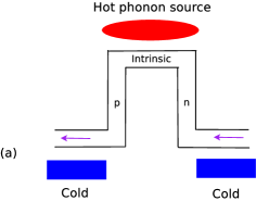
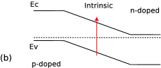
In the following discussions we specifically consider a -- junction made of “extremely narrow-gap semiconductors”. The structure is depicted in Fig. 1a, for the case of converting thermal to electrical energy. It can be viewed as an analog of the -- photodiode, where photons are replaced by phonons, i.e., the phonon-assisted inter-band transitions lead to current generation in the junction. The device can also be used to e.g. cool the thermal terminal via the electric current between the electronic terminals. We focus on the situation where single-phonon assisted inter-band transitions are allowed. (The electronic band gap is hence required to be smaller than the phonon energy). Such processes may play a significant role in the transport across the junction whereas the transition rates of multi-phonon processes are much smaller. In semiconductors, the optical phonon energy is usually in the range of meV. There are several candidates with such small band gaps: (i) Gapless semiconductors resulting from accidental band degeneracy in solid solutions, such as Pb1-xSnxTe and Pb1-xSnxSe.gaplesssemi At a certain mole fraction the band gap closes, around which it can be very small. (ii) Gapless semiconductors originating from band inversion, such as HgTe and HgSe.gaplesssemi The band gap can be tuned via the quantum-well effect in the superlattices composed of a gapless semiconductor and a normal semiconductor without band inversion.bhz An example is the HgTe/CdTe superlattices with a tunable band gap.balents (iii) Multilayers (superlattices) of “topological” insulators with ordinary insulator layers sandwiched between the topological ones.burkov For example, in Bi2Te3/Si superlattices the energy gap can be tuned by varying the thickness of the topological and ordinary layers.burkov A significant merit of superlattices is that the lattice thermal conductivity along the growth direction can be much smaller than both of the two bulk constituents. For example, the Si/Ge superlattices have a thermal conductivity about two orders of magnitude smaller than the bulk values.lowkl We also point out that the same idea can be applied to devices where the role of optical phonons is played by other bosons. If the energy of such bosons is higher the requirement for small band gap can be softened.
For simplicity we consider a linear junction where the conduction band edge varies linearly in the intrinsic region with the coordinate along the junction from to as
| (5) |
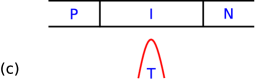
with being the band gap.Sze We set so that the -doped (-doped) region is at the left (right) side of the junction [see Fig. 1b]. These electronic terminals can have temperatures different from that of the thermal terminal. It is favorable to bend the two electronic terminals away from the thermal one so that they will be better thermally isolated from the thermal terminal and from each other [see Fig. 1a]. Another possibility is a “thermal finger” for the boson bath [Fig. 1c], which can be well isolated from the electronic leads.
II.2 “Ideal” figure of merit
We start by considering only the phonon-assisted transport, ignoring the phononic thermal conduction and the normal diode transport. The phonon-assisted inter-band transitions generate current flow in the junction. In the linear-response regime, the thermoelectric transport equations are written as3t
| (6) |
Here and are the electronic charge and heat currents flowing between the two electronic terminals, is the electronic charge, is the heat current from the thermal terminal to the two electronic ones, is the conductance in the inelastic channels, is related to the electronic heat conductance between the electronic terminals, and is that between the thermal terminal and the electronic ones. The transport coefficients , , and are related to the currents induced by the temperature differences (thermopower effect) and the current-induced temperature differences (refrigerator and heater effects). () is the chemical potential (temperature) difference between the two electronic terminals, and is the difference between the temperature of the thermal terminal and the average temperature of the two electric ones, with , , and being the temperatures of the left, right electronic terminals, and the phonon terminal, respectively. With these definitions of , , and , the Onsager reciprocal relationships are satisfied. In such a setup, as found in Ref. 3t, , the three-terminal Seebeck coefficient and figure of merit are, when and are neglected,
| (7) |
respectively. To obtain the transport coefficients and the figure of merit, we need to calculate the phonon-assisted currents through the system.
The Hamiltonian of the inter-band electron-phonon coupling ismore
| (8) |
where is the volume of the system, is the phonon branch index, () runs through the valence (conduction) band indices, is the matrix element of the electron-phonon coupling, and () is the electron (phonon) creation operator. Due to momentum (when valid) and energy conservations, phonons involved in such processes will be in a small energy range. For indirect-band semiconductors and with momentum conservation, these phonons can be acoustic as well as optical ones. For simplicity and definiteness, we consider a direct-band semiconductor system and assume that the contribution from the optical phonons is the dominant one. From Eq. (8), the net electron-hole generation rate per unit volume, , is given for single-phonon transitions by the Fermi golden rule as
| (9) | |||||
where
| (10) | |||||
Here, , , and are the electron and phonon energies when the two systems are uncoupled, and are the nonequilibrium distributions of electrons and phonons in the intrinsic region, with due to energy conservation. According to Ref. shockley, , when the length of the intrinsic region is sufficiently smaller than the carrier diffusion length, the electronic distribution in the conduction (valence) band in the intrinsic region can be well approximated as the distribution in the -doped (-doped) electronic terminal.shockley Similarly the phonon distribution is almost the same as that in the thermal terminal when the contact between the intrinsic region and the thermal terminal is good. Finally, a small amount of disorder which always exists in real systems and relaxes the momentum conservation can enhance the phonon-assisted inter-band transitions.
The transport coefficients are determined by studying the currents at a given bias and/or a temperature difference. The key relation is the continuity equation,shockley ; closed
| (11) |
where () are the electron and the hole densities in the conduction and valence bands, and are the equilibrium values of those densities. are the charge currents, are the charges of the electron and the hole, are the carrier lifetimes limited by the recombination processes other than the phonon-assisted ones that have already been taken into account in , and is the net carrier density generation rate given in Eq. (9). The currents , which consist of diffusion and drift parts, are
| (12) |
where and are the mobilities and the diffusion constants, respectively. They are related by the Einstein relation, . is the built-in electric field in the intrinsic region.
If Boltzmann statistics for the electrons can be assumed everywhere, the net generation rate will depend on very weakly such that its spatial dependence can be ignored. In this situation, the total carrier densities can be divided into two parts, where are the spatially-independent carrier densities generated by the phonon-assisted inter-band transitions and are the “normal” densities in the junction, determined by the continuity equation with . Similarly, the current is divided into two parts, . The current in the normal diode channel can be obtained from Eqs. (11) and (12) with proper boundary conditions, yielding the celebrated rectification current-voltage relation,
| (13) |
with being the saturated currents. Here is the density of the minority carrier and is its diffusion length.shockley
Inserting into Eq. (12), one obtains the currents in the phonon-assisted channelnote11
| (14) |
In the linear-response regime,
| (15) | |||||
where and are the equilibrium distribution functions of the electrons and the phonons, respectively, and . Consequently
| (16) |
where is the equilibrium transition rate [defined in Eq. (15)] and the average is defined in Eq. (4) with
| (17) | |||||
The above results are very similar to those obtained in Ref. 3t, : due to the inelastic nature of the transport, the carrier energies at the and terminals are different; the heat transferred between the two terminals is the average one , whereas the energy difference is transferred from the thermal terminal to the two electronic ones. This is also manifested in the way the temperature differences are coupled to the heat flows3t in Eq. (15), ensuring the Onsager relations. An important feature is that the three-terminal Seebeck coefficient, , is negative definite since . In contrast, the two-terminal Seebeck coefficient, , does not possess this property. It can be positive or negative due to the partial cancelation of the contributions from electrons and holes, whereas there is no such cancelation for [see Eq. (16)]. Equation (16) is a generalization of the results in Ref. 3t, where there was only a single microscopic energy channel. When many inelastic processes coexist, the contribution of each process is weighed by its conductance. From Eqs. (7) and (16), we find that the “ideal” three-terminal figure of merit is
| (18) |
For a single microscopic energy channel system where is fixed, this figure of merit goes to infinity.3t When there are many many such energy channels, it becomes finite due to the nonzero variance of . We estimate the figure of merit when and . Here is the average phonon energy and is the effective bandwidth (i.e., the variance of due to spectral dispersion) of the involved phonons. From Eqs. (16) and (17) one finds that the variance of is limited by or whichever is smaller. For example, when the effective phonon bandwidth is much smaller than , the variance is rather limited by . In the situations where , the numerator in Eq.(18) is much larger than the denominator. The “ideal” figure of merit can be very high thanks to the electronic band gap when or the narrow bandwidth of the optical phonons . However, in realistic situations, as often happens, the parasitic heat conduction is another major obstacle to a high figure of merit. This will be analyzed in the next subsection.
II.3 Realistic figure of merit
Besides the phonon-assisted transport channel, there is the normal diode channel which is dominated by the (elastic) barrier transmission and the diffusion of minority carriers. It contributes to , , and as well. In addition there are the “parasitic” heat currents carried by phonons flowing between the two electronic terminals and those from the thermal terminal to the electronic ones. Taking into account all these, the thermoelectric transport equations are written as
| (19) |
Here, is the total heat current between the two electronic terminals which consists of the electronic and the phononic contributions; is the total heat current flowing out of the thermal terminal to the two electronic ones with being the purely phononic part. Finally, , , and are the contributions to the transport coefficients from the normal diode (elastic) channel, and and are the heat conductances of phonons flowing between the two electronic terminals and those flowing from the thermal terminal to the two electronic ones, respectively. Note that the elastic channel does not contribute to and which are solely related to the inelastic processes. The three-terminal figure of merit can be obtained by optimizing the efficiency of a refrigerator working at but with finite and . This figure of merit is3t
| (20) |
which is equivalent to Eq. (3). The diode conductance is . A high figure of merit requires which is not difficult to achieve according to the analysis in the next subsection (II.4). In such a situation and when or , i.e., when the energy width due to or gives a much weaker limitation to than , one finds from Eq. (20)fotno1
| (21) |
Estimations carried out in Sec. II.4 indicate that there are parameter regimes where the figure of merit Eq. (20) can be greater than the usual two-terminal ones in the same material. We repeat that, unlike the two-terminal case, the thermal conductance between the electronic terminals, does not affect the three-terminal figure of merit.
Often and are of the same order of magnitude. We note that and are small in several gapless semiconductors such as PbSnTe, PbSnSe, BiSb, HgTe, and HgCdTe. In addition, superlattice structures (and other planar composite structures) usually have much lower and along the growth direction than the bulk materials.spMahan The geometry where the electric current flows along that direction is promising for high figures of merit.
II.4 Estimation of the figure of merit
We defined () as the carrier lifetimes due to recombination processes other than the phonon-assisted ones that have already been taken into account in [see Eq. (9)]. The carrier lifetimes due to the phonon-assisted processes, for the electrons and for the holes, satisfy the detailed balance relations in the intrinsic region. Here is the electron (hole) density in that region and is the equilibrium transition rate per unit volume defined in Eq. (15). The transition between minibands in semiconductor superlattices is usually dominated by the phonon-assisted processes in the dark limit when the miniband gap is smaller than the phonon energy.ridley We introduce the parameter to write . This parameter is governed by the electron-phonon interaction strength, being of order unity when such a coupling is strong as is the case for some III-V (and other) semiconductors, or smaller (it will be taken as below).ridley Inserting this into Eq. (16) one finds
| (22) |
where stands for the length of the intrinsic region which will be taken to be much smaller than the diffusion length . shockley In Eq. (22) we have chosen [defined in Eq.(5)] to be close to 1 which amounts to high doping density in the and doped regions. The elastic conductance is the slope of the - rectification characteristics, Eq. (13), at ,
| (23) |
with denoting the carrier diffusion length. The majority carrier densities (doping densities) in both the and regions are taken to be . It follows then that
| (24) |
A small ratio can be easily achieved since and . Therefore the contribution of is not the main obstacle for a high figure of merit in this device.
For with (the effective width of the relevant energy band) and being much smaller than (the typical phonon energy), the figure of merit is given by Eq. (21). The phononic heat conductance is, as usual, the least known and an extremely important obstacle for increasing . can be reduced, in principle, by engineering the interfaces. Even without such improvement, according to the geometry where is the bulk phonon thermal conductance across the junction. In the relevant regime . From Eq. (22) we then obtain
| (25) |
We shall introduce yet another parameter to characterize the ratio with being the electron thermal conductance in a doped sample of the same geometry and size as the junction, with doping density . The temperature dependence of the ratio varies with the doping, structure, and temperature. The temperature dependence is assumed to be of the form with being a constant. A temperature-independent prefactor parameter is then introduced. We further assume that the transport properties in the and regions are similar (up to signs). The Wiedemann-Franz law implies that where denotes the electrical conductance in the doped sample and for Boltzmann statistics. According to Ref. shockley, , when and is small. Using Eq. (23) one can write . The figure of merit is then estimated as
| (26) | |||||
If the temperature dependence comes mainly from the first two factors then a high figure of merit can be obtained for . For large the three-terminal figure of merit can be larger than the two-terminal one. The power factor of the device, , can be estimated similarly.
An especially appealing setup exploiting the topological-insulator–ordinary-insulator–superlattices, can be built as follows (taking the superlattice Bi2Te3/Si as an example): On the front and back surfaces of each thin Bi2Te3 layer there are protected surface states with a gapless Dirac-cone like spectrum.TIreview Tunneling between the two surfaces opens a gap in the spectrum of each surface band.burkov In superlattices these states form a pair of conduction and valence minibands where the band gap can be controlled via the thickness of the two types of layers [for details see Ref. burkov, and footnote fotnot1, ]. As the energy of the optical phonon in Si is much larger than that in Bi2Te3, the optical phonons in Si layers are well localized in these layers. So do the optical phonons in the Bi2Te3 layers. Similarly, due to the significant mismatch of the mechanical properties of the two types of layers, the acoustic phonons also have difficulty in being transmitted across the interfaces. The phononic thermal conductivity along the growth direction is then considerably reduced. It should be smaller than the values for both materials in the bulk.lowkl On the other hand, the phononic heat conductivity within each thin layer of Si is large. At T=300 K, the former is 1.5 Wm-1K-1,bitekl whereas the latter is about Wm-1K-1.sikl When the electric current is along the growth direction, the small phononic heat conductance along this direction greatly reduces the parasitic heat conduction and benefits the figure of merit. On the other hand within each Si layer phonons are transferred efficiently from the thermal terminal to the system, which is good for enhancing the output power of the device.
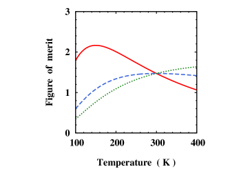
We now estimate the figure of merit of the device using the example of the semiconductor made of the Bi2Te3/Si superlattice. We shall use the transport parameters of bulk Bi2Te3 to do the estimation although the superlattice should have better thermoelectric performance.bitesl First tune the superlattice structure to make with being the energy of the optical phonon in Si which is about 60 meV [see Ref. LB, ] (equivalent to about 700 K). We will choose . In Bi2Te3 with cm-3, one finds from Ref. bitekl, that at 300 K. This determines the parameter to be . Using these parameters we calculate and plot the figure of merit as a function of temperature in Fig. 2 for a practically achievable value and a modest value of . In the calculation we ignored the temperature dependence of and . The results are computed for three situations with , and . It is seen that the figure of merit with the several underestimations made, can be larger than 1 around room temperature for all the three situations, indicating potential usefulness. Finally we note that the same strategy and analysis can also be applied to the superlattice made of an inverted-band gapless semiconductor and a normal semiconductor, where the band gap can be tuned via the quantum well effectbhz and the normal semiconductor can be chosen to have the proper optical phonon frequency and the high thermal conductivity to enable better thermoelectric performance.
III Conclusions and discussions
We proposed and studied a thermoelectric device using the phonon bath as an example. The scheme is based on the “three-terminal” geometry of thermoelectric applications,3t0 ; 3t1 ; 3t2 ; 3t ; 3t3 where inelastic processes play a crucial role. It has been shown that a high thermoelectric figure of merit can be achieved in this geometry in several nanosystems,3t where only one microscopic energy channel in which the relevant electronic energy is fixed, is available. In this paper we derived the figure of merit for the multiple energy channel case. We find that, when only the inelastic processes are considered, the figure of merit is the ratio of the square of the mean value of energy difference between final and initial states to its variance with the average weighed by the conductance of each microscopic process. A small variance in the energy change is then favorable for a high figure of merit. To achieve such a good energy selection, one can use either the electronic band gap, , for electrons or the narrowness of the phonon band, , for phonons. The realistic figure of merit including other processes, Eq. (3), is also discussed. It is found that a strong carrier-boson coupling as well as the dominance of the inelastic transport and a small purely phononic thermal conductivity between the phonon terminal and the electronic ones, are necessary for a high figure of merit. The suppression of the elastic transport can be achieved with a semiconductor junction,shockley while the coupling is strong when the bosons are, e.g., phonons, electron-hole pair excitations, etc.. Thanks to those, the proposed three-terminal device can have a figure of merit higher than that of the usual two-terminal device made of the same material.
In comparison with the existing literature, M-S suggested a narrow electronic band for elastic two-terminal transport to achieve high values of . When this scheme is generalized to inelastic processes where the initial and final energies are different, high values of are possible when the distribution of the average energy (measured from the common chemical potential) is narrow in the two-terminal geometry. In the three-terminal situation a narrow distribution of plays a crucial role. The latter can also be achieved by controlling the initial and final electronic states by a barrier higher enough than , or in a small system with a few initial and final states with fixed , as in Refs. 3t, ; 3t2, ; 3t3, , or, for example, via the narrow bandwidth of optical phonons. Finally, we note the analogy of the suggested configuration, which may convert thermal to electrical energy, and a photovoltaic device.
Acknowledgments
OEW acknowledges the support of the Albert Einstein Minerva Center for Theoretical Physics, Weizmann Institute of Science. This work was supported by the BMBF within the DIP program, BSF, by ISF, and by its Converging Technologies Program.
References
- (1) T. C. Harman and J. M. Honig, Thermoelectric and Thermomagnetic Effects and Applications, (McGraw-Hill, New-York, 1967); H. J. Goldsmid, Introduction to Thermoelectricity (Springer, Heidelberg, 2009).
- (2) G. S. Nolas, J. Sharp, and H. J. Goldsmid, Thermoelectrics: Basic Principles and New Materials Development (Springer, Berlin, 2001).
- (3) G. J. Snyder and E. S. Toberer, Nat. Mater. 7, 105 (2008).
- (4) M. S. Dresselhaus, G. Chen, M. Y. Tang, R. Yang, H. Lee, D. Wang, Z. Ren, J.-P. Fleurial, and P. Gogna, Adv. Mater. 19, 1043 (2007); A. Shakouri, Ann. Rev. of Mater. Res. 41, 399 (2011).
- (5) G. D. Mahan and J. O. Sofo, Proc. Natl. Acad. Sci. 93, 7436 (1996).
- (6) J. M. Ziman, Principles of The Theory of Solids, 2nd ed. (Cambridge University Press, Cambridge, 1995), Secs. 7.7-7.9.
- (7) L. D. Hicks and M. S. Dresselhaus, Phys. Rev. B 47, 12727 (1993); ibid., 16631 (1993); R. Venkatasubramanian, Phys. Rev. B 61, 3091 (2000).
- (8) R. Venkatasubramanian, Phys. Rev. B 61, 3091 (2000); J.-K. Yu, S. Mitrovic, D. Tham, J. Varghese, and J. R. Heath, Nat. Nanotechnol. 5, 718 (2010).
- (9) See, e.g., J. Cai and G. D. Mahan, Phys. Rev. B 78, 035115 (2008); J. Zhou and R. Yang, Phys. Rev. B 82, 075324 (2010); P. Kratzer, V. M. Fomin, B. Hülsen, and M. Scheffler, arXiv:1011.0324.
- (10) T. E. Humphrey and H. Linke, Phys. Rev. Lett. 94, 096601 (2005).
- (11) J. Zhou, R. Yang, G. Chen, and M. S. Dresselhaus, Phys. Rev. Lett. 107, 226601 (2011); C. Jeong, R. Kim, and M. Lundstrom, J. Appl. Phys. 111, 113707 (2012).
- (12) I. P. Zvyagin, Phys. Stat. Sol. (b) 58, 443 (1973).
- (13) B. Rutten, M. Esposito, and B. Cleuren, Phys. Rev. B 80, 235122 (2009); B. Cleuren, B. Rutten, and C. Van den Broeck, Phys. Rev. Lett. 108, 120603 (2012).
- (14) O. Entin-Wohlman, Y. Imry, and A. Aharony, Phys. Rev. B 82, 115314 (2010).
- (15) R. Sánchez and M. Büttiker, Phys. Rev. B 83, 085428 (2011).
- (16) J. H. Jiang, O. Entin-Wohlman, and Y. Imry, Phys. Rev. B 85, 075412 (2012).
- (17) B. Sothmann, R. Sánchez, A. N. Jordan, and M. Büttiker, Phys. Rev. B 85, 205301 (2012).
- (18) There are some similar ideas and experimental works in the literature, e.g., H. L. Edwards, Q. Niu, and A. L. de Lozanne, Appl. Phys. Lett. 63, 1815 (1993); H. L. Edwards, Q. Niu, G. A. Georgakis, and A. L. de Lozanne, Phys. Rev. B 52, 5714 (1995); V. S. Khrapai, S. Ludwig, J. P. Kotthaus, H. P. Tranitz, and W. Wegscheider, Phys. Rev. Lett. 97, 176803 (2006); S. Zippilli, G. Morigi, and A. Bachtold, Phys. Rev. Lett. 102, 096804 (2009); J. R. Prance, C. G. Smith, J. P. Griffiths, S. J. Chorley, D. Anderson, G. A. C. Jones, I. Farrer, and D. A. Ritchie, Phys. Rev. Lett. 102, 146602 (2009); A. N. Jordan, B. Sothmann, R. Sánchez, and M. Büttiker, Phys. Rev. B 87, 075312 (2013).
- (19) Semiconductors, Landolt-Börnstein, New Series, Vol. 22a, ed. by O. Madelung (Springer-Verlag, Berlin, 1987).
- (20) See, e.g., R. Mickevičius and A. Reklaitis, J. Phys.: Condens. Matter 2, 7883 (1990).
- (21) I. M. Tsidilkovski, Electron sepctrum of gapless semiconductors (Springer-Verlag, Berlin, 1997).
- (22) B. A. Bernevig, T. A. Hughes, and S.-C. Zhang, Science 314, 1757 (2006).
- (23) G. B. Halász and L. Balents, Phys. Rev. B 85, 035103 (2012).
- (24) A. A. Burkov and L. Balents, Phys. Rev. Lett. 107, 127205 (2011).
- (25) D. G. Cahill, W. K. Ford, K. E. Goodson, G. D. Mahan, A. Majumdar, H. J. Maris, R. Merlin, and S. R. Phillpot, J. Appl. Phys. 93, 793 (2003).
- (26) S. M. Sze and K. K. Ng, Physics of Semiconductor Devices (John Wiley and Sons, 2007).
- (27) There are other possible inter-band transition processes, such as the defect trap states mediated inter-band transitions (the Shockley-Read-Hall processes). Those are higher-order processes of which the rate should be smaller. There are also the Auger processes due to the inter-band Coulomb interaction. The Auger processes are important for narrow-band semiconductors such as InSb. As far as we know there is no theoretical work devoted to the comparison of the Auger processes and optical-phonon-induced inter-band transitions when the band gap is smaller than the optical-phonon energy. However, for the superlattice structures studied in this work, the transition should be very much like the inter-subband transitions in semiconductor quantum wells. In the latter, experimental and theoretical investigations [see M. Woerner and T. Elsaesser, Ultrafast Nonequilibrium Dynamics of Intersubband Excitations, in Ultrafast Phenomena in Semiconductors, ed. K.-T. Tsen (Springer-Verlag, New York, 2001), p.127] revealed that the optical-phonon interaction (especially confined and interface phonons) dominates the inter-subband scattering. This supports our assumption that the inter-miniband transitions in the superlattice-based device are dominated by the optical-phonon processes. Moreover, as the Auger processes conserve the total energy of the electronic system, they will not affect the transfer of energy between the electronic system and the thermal bath. Hence, although we do not include the Auger processes in the theoretical treatment, they will not spoil the functionality and performance of the device.
- (28) W. Shockley, Electrons and Holes in Semiconductors (D. Van Nostrand Company, Inc., New York, 1950).
- (29) K. Tarettou, U. Rau, and J. H. Werner, Appl. Phys. A 77, 865 (2003).
- (30) Here we have used certain simplifications. The consideration only holds for the central part of the intrinsic region, while the situation near the boundaries is more complicated. However, this is not supposed to change the results considerably.closed
- (31) Generally one can estimate the figure of merit as when . We mostly assume that is the smallest among the three.
- (32) J. O. Sofo and G. D. Mahan, Appl. Phys. Lett. 65, 2690 (1994); D. A. Broido and T. L. Reinecke, Phys. Rev. B 51, 13797 (1995); P. Hyldgaard and G. D. Mahan, Phys. Rev. B 56, 10754 (1997).
- (33) B. K. Ridley, Quantum Processes in Semiconductors (Oxford, 1993).
- (34) M. Z. Hasan and C. L. Kane, Rev. Mod. Phys. 82, 3045 (2010); X.-L. Qi and S.-C. Zhang, Rev. Mod. Phys. 83, 1057 (2011).
- (35) In Ref. burkov, it is shown that the gap is where and are the tunneling rates through the topological and the ordinary insulator layer, respectively. They (and the band gap) can be tuned in a large range via the thickness of these layers.
- (36) C. B. Satterthwaite and R. W. Ure, Jr., Phys. Rev. 108, 1164 (1957).
- (37) G. A. Slack, J. Appl. Phys. 35, 3460 (1964).
- (38) R. Venkatasubramanian, Phys. Rev. B 61, 3091 (2000); M. N. Touzelbaev, P. Zhou, R. Venkatasubramanian, and K. E. Goodson, J. Appl. Phys. 90, 763 (2001).