Structural ordering driven anisotropic magnetoresistance, anomalous Hall resistance and its topological overtones in full-Heusler Co2MnSi thin films
Abstract
We report the evolution of crystallographic structure, magnetic ordering and electronic transport in thin films of full-Heusler alloy Co2MnSi deposited on (001) MgO with annealing temperatures (). By increasing the from 300∘C to 600∘C, the film goes from a disordered nanocrystalline phase to ordered and finally to the ordered alloy. The saturation magnetic moment improves with structural ordering and approaches the Slater-Pauling value of per formula unit for = 600∘C. At this stage the films are soft magnets with coercive and saturation fields as low as 7 mT and 350 mT, respectively. Remarkable effects of improved structural order are also seen in longitudinal resistivity () and residual resistivity ratio. A model based upon electronic transparency of grain boundaries illucidates the transition from a state of negative to positive with improved structural order. The Hall resistivity () derives contribution from the normal scattering of charge carriers in external magnetic field, the anomalous effect originating from built-in magnetization and a small but distinct topological Hall effect in the disordered phase. The carrier concentration () and mobility () have been extracted from the high field data. The highly ordered films are characterized by and of 1.19 1029 m-3 and 0.4 cm at room temperature. The dependence of on indicates the dominance of skew scattering in our films, which shows a monotonic drop on raising the . The topological Hall effect is analyzed for the films annealed at 300∘C. We find maximum topological contribution to Hall resistivity around 0.5 T while it approach to zero with increasing magnetic field. The anisotropic magnetoresistance changes its sign from positive to negative as we go from as deposited to 600∘C annealed film suggesting a gradual increase in the half-metallic character.
I INTRODUCTION
Although discovered a century ago by F. Heusler, the compounds which bear his name have captured much attention in recent years due to their fascinating properties which include magneto-stuctural,Kainuma magneto-optical,Krenke and magneto-caloric phenomena,Engen large thermo-electricityBosu and heavy fermion superconductivity.Wernick Recently, a new property has been predicted in which spin-polarized edge and surface states are topologically protected against impurity scattering, known as topological insulator.Chadov ; Lin The coexistence of superconductivity and a magnetically ordered state have also been reported for Heusler alloys containing rare earth elements.Kierstead A certain class of full-Heusler alloys are particularly important for spintronics applications. The spin-polarized tunneling, which incorporates the imbalance between the density of states (DOS) of two spin states in the conduction band, controls the performance of devices like magnetic tunnel junctions and spin valves, and can be improved significantly if the conduction electrons are fully spin-polarized. These materials are characterized by a spin-split conduction band with a clear energy gap for the up and down spin states, and the Fermi level () being located in one of them. This property of the electronic structure is called half-metallicity and a large number of Heusler alloys have been predicted to be half-metals. Although there are other compounds such as La1-xSrxMnO3 Park and CrO2Yji with measured spin polarization at low temperatures, but they are not suitable for ambient temperature applications because of their low ( K) Curie temperature (). The Heusler alloys, which have very high , are much suitable for spintronics applications, provided the spin-polarized nature of the conduction band can be retained in the films of these materials. However, due to atomic and/or antisite disorder, the degree for spin polarization in epitaxial films is found to be smaller than those obtained from various band structure calculations. Additionally, there is a reduction in spin polarization at the surfaces due to surface reconstruction,Ristoiu and disorderKautzky present between different sublattices. Therefore, studies of atomic and antisite disorder, surface reconstruction and spin polarization in thin films of Heusler alloys is a challenging but worthwhile problem to pursue.
Amongst all Heusler alloys, the Co-based full-Heusler compounds are attractive due to their high and high magnetic moment per formula unit (f.u.). The full-Heusler alloy Co2MnSi (CMS) belongs to the same family with = 985 KFujii and a large minority-spin band gap of 0.4 eV. While, a large number of full-Heusler alloy thin films have been grown on semiconductors like Si,Zander Ge,Kasahara and GaAs;Wang there are few reports on the films grown on oxide substrates such as Al2O3,Singh ; Schneider MgOSchneider ; Pandey ; Schneider2 and SrTiOAnupam ; Himanshu1 Various deposition techniques such as laser ablation,Wang ; Schneider ; Pandey ; Anupam ; Himanshu1 ; Rout sputteringGeiersbacha ; Raphael ; Kammerer ; Kim and molecular beam epitaxyAmbrose are in use for the growth of such films under varying conditions of growth. It is well-known that the choice of the deposition temperature, growth conditions, and substrates can significantly alter the structural, magnetic, and electronic properties of thin films.
Here our focus is to carryout an in-depth study of the electronic transport and magnetism of CMS films grown on (001) MgO by a single target pulsed laser ablation technique (PLD). The lattice parameter ( 0.5655 nm) of CMS matches quite well with the face diagonal () of MgO. The lattice misfit [] between the CMS and MgO is . It should be noted that the first principle calculations by Kandpal et al.Kandpal show that the strain 5% does not alter the band structure significantly. Thus, the charge transport in these films should behave in the same way as that of the bulk samples. The fabrication of stoichiometric films from an alloy target is the key strength of PLD. This technique relies on the formation of a local superheated region on the target, which then explodes as a plasmonic plume maintaining the stoichiometry of the target. The high thermal conductivity of elemental metals, however, hinders the formation of a superheated spot on the target and the material is removed by splashing, rather than ablation. Therefore, the parameters such as laser energy density, pulse repetition rate, and target-to-substrate distance need to be optimized very carefully.
The half-metallic character and saturation magnetization of Heusler alloys are linked to atomic structure and crystallographic ordering in the material. In thin films, the optimum realization of these two parameters is affected by lattice strain, interfacial metallurgy and surface roughness. The Heusler compound CMS crystallizes in the cubic space group with type ordering. This structure can be built from a zinc blende-type sublattice of one Co and one Si. The second Co fills the tetrahedral holes of the structure whereas Mn occupies the octrahedral holes. Theoretical calculations show that a small variation from this ordered arrangement of atoms can significantly affect the electronic and magnetic properties of the Heusler compounds. The greater atomic ordering is realized when the compound is synthesized at high temperatures. For electronic applications, it is desirable to grow films at as low a temperature as possible to ensure high surface smoothness and integration with other device process steps. Here we report the evolution of atomic ordering in CMS films deposited on (001) MgO at 200∘C and subsequently annealed at several temperatures. The extent of atomic ordering has been monitored by two magneto-transport measurements; namely Anisotropic magnetoresistance (AMR) and Hall effect, which respectively yield quantitative information about the degree of spin polarization, saturation magnetization (MS) and spin chirality. These data have been supported by direct measurement of magnetization, longitudinal resistivity and crystallographic structure. This paper comprises of following sections, out of which the introduction has been presented already in Sec. I. The sample preparation and various measurement procedures are given in Sec. II. All the results and their discussions are given in Sec. III, which deals with the structural and elemental characterization in addition to magnetic ordering and electronic transport in the CMS films. The anomalous Hall effect (AHE), topological Hall effect (THE), and AMR results are described in Sec. IV and finally, the conclusions drawn from these studies are given in Sec. V.
II EXPERIMENTAL DETAILS
40 nm thick films of CMS were deposited by pulsed laser ablation of stoichiometric target of the alloy. A KrF excimer laser (wavelength = 248 nm and pulse width 20 ns) was used for the film deposition. The target was prepared by arc melting a mixture of the constituents (99.99% pure) in argon atmosphere. The alloy ingot was re-melted many times and then annealed at 10000C for 24 hours to secure homogenization. Prior to the annealing, the target was wrapped with tantalum foil in order to avoid any undesired oxidation and then placed in a quartz tube, which was subsequently evacuated and sealed. The resulting target has L structure and elemental stoichiometry in the ratio of 2:1:1 for Co, Mn, and Si, respectively as confirmed by X-ray diffraction (XRD) and energy dispersive X-ray analysis (EDAX). A Perfect site order can usually be achieved by preparing the films on lattice matched substrates at high temperatures. This is often undesirable for devices where requirement of smooth surfaces, sharp interfaces and minimized inter-diffusion are the key for performance. We used a growth temperature of 200∘C followed by one hour annealing at = 300, 400, 500, and 600∘C to enhance crystallization and ordering in the films. The growth and post-deposition annealing were carried out in an all-metal-seal high vacuum chamber equipped with a Ti-getter pump and an ultra high vacuum compatible substrate heater which could heat the samples to 850∘C. Prior to the thin film deposition, the MgO substrates were annealed at 800∘C for 30 minutes to allow surface reconstruction. Afterwards, the temperature was lowered to 200∘C to commence the growth. The crystallographic structure of the films was characterized in -2, , , and grazing incidence X-ray diffraction (GIXRD) modes using a PANalytical X’Pert PRO X-ray diffractometer equipped with a Cu source. From the simulation of X-ray reflectivity (XRR) curves by a genetic algorithm, we estimated the film thickness. The surface roughness of the films were obtained by XRR and atomic force microscopy (AFM). The high resolution field emission scanning electron microscopy (FESEM, Model: SUPRA40VP) and EDAX were used to check the homogeneity, stoichiometry and uniformity of the thin films. For room temperature magnetization measurements with both in-plane and out-of-plane field orientations, we have used a vibrating sample magnetometer. For the electrical measurements, samples were patterned in a four-probe geometry using ion milling through a stainless steel shadow mask and the silver pads for electrical contact were deposited by thermal evaporation. The resistivity and AMR measurement were performed in constant current mode using precision programmable dc current source (Keithley 224), digital temperature controller (Scientific Instruments Inc model 9650), and nanovoltmeter (Keithley 2182). For Hall measurement, samples were patterned into standard six probe Hall bar geometry and measured in Physical Property Measurement System (PPMS, Quantum Design).
III RESULTS AND DISCUSSION
III.1 Structural and elemental characterization
The crystal structure of the ordered full-Heusler alloy CMS consists of four fcc sublattices with Co atoms at (1/4, 1/4, 1/4) and (3/4, 3/4, 3/4), the Mn atom at (0, 0, 0), and the Si atom at (1/2, 1/2, 1/2 ) in Wyckoff coordinates. These alloys are prone to antisite disorder. A complete disorder involving the mixing of all site, results in the A2 structure type with reduced symmetry . The most frequently occuring disorder type is B2, where the Mn and Si atoms at 4a and 4b positions are interchanged randomly resulting in symmetry. This type of disorder, in which the Co positions are not affected, changes the degree of spin polarization marginally.Kudryavtsev Additionally, DO3 disorder can take place, which consists of random exchange between Co and Mn atoms. Figure 1(a) shows the -2 XRD profiles of CMS films annealed at different temperatures. The as-deposited film does not show any resolvable Bragg peaks suggesting a nano-crystalline nature. However, with the increase in , the diffraction lines appear and their intensity and sharpness become prominent. The diffraction profile of 600∘C annealed film shows intense and reflections of the cubic phase. The ratio of the intensities of the and Bragg peaks, which is a measure of the degree of crystallographic order on the Co sites,webster also increases with . Figure 1(b) shows the GIXRD spectra for 600∘C annealed film taken to check the presence of superlattice, that governs the ordering of the Mn and Si sublattices and fundamental diffraction line, which confirms the presence of ordering in the films. This is also earlier confirmed by taking the scans for and peaks of the CMS film.Pandey The values for the and planes of the CMS film are shifted by 450 with respect to those of the MgO planes, clearly demonstrates the fourfold symmetry of cubic phase of 600∘C annealed film. Rocking curves of the films have a full width at half maximum (FWHM) of 0.4, indicating a high-quality epitaxial growth. A typical rocking curve about CMS peak is shown in Fig. 1(c). The FWHM of these peaks decreases with the increase in , which suggests that the (00) texture improves with increasing . Figure 1(d) shows the variation of and ordering parameter with calculated using the formulation given by Takamura et al.Takamura These parameters give the measure of the atomic ordering in the ordered/diordered state of the Heusler alloys films.
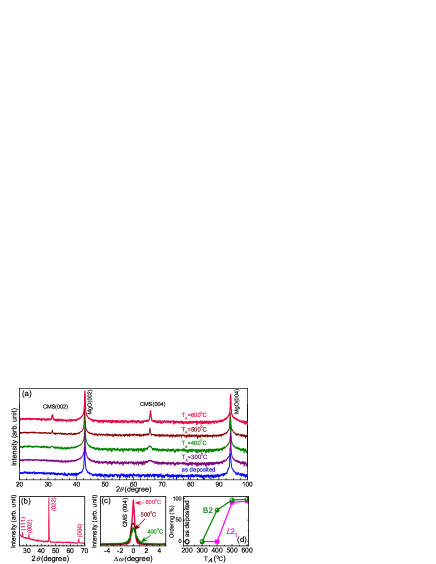
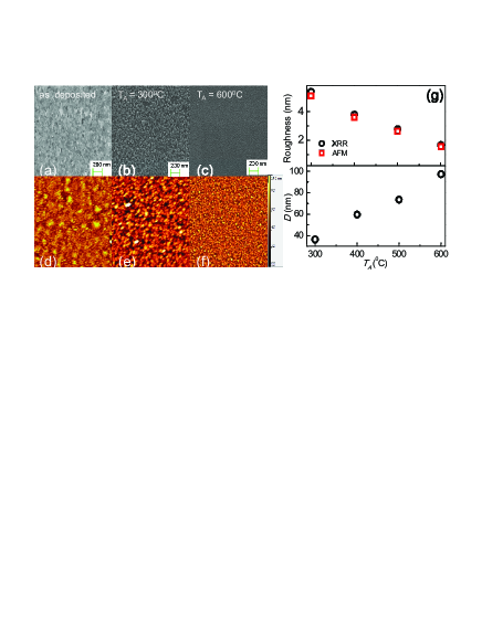
The SEM micrographs of CMS films processed under different conditions are presented in Fig 2(a-c). These surfaces are devoid of any particulate matter, which is commonly seen in PLD grown films if the conditions are not optimized. We also note that the films become smoother as increases. The non-contact AFM images of the above mentioned films are shown in Fig. 2(d-f). The roughness obtained from AFM scans and XRR measurements are compared in Fig. 2(g) (upper panel), while the lower panel shows the variation of grain size with estimated by using Debye-Scherrer method. As the increases the grain size increase to attain orientation.
In summary, these PLD grown films show three characteristically different structural states; (i) the as-prepared films having nanocrystalline phase with strong site disorder, (ii) the nanocrystalline phase with a substantial degree of site order inside the grains, and (iii) the crystalline phase with high degree of site order and structural long-range order.
III.2 Evolution of magnetic order on annealing
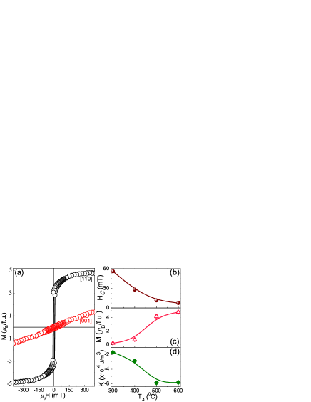
The magnetization () vs field () loops of the 600∘C annealed film taken at room temperature in out-of-plane and in-plane field directions are shown in Fig. 3(a). We clearly see that the films are magnetically soft with in-plane magnetization easy axis, coercive field () 7 mT, and almost square loops reaching saturation within 300 mT. The saturation magnetic moment extracted from these data is 4.780.19 /f.u., which is in accordance with the theoretical predictions.Galanakis The of the films depends on the internal stresses, grain size, crystal structure, magnetic inhomogeneities, surface roughness, and thickness. The as-deposited film shows a much higher compared to annealed films. The variation of with is shown in Fig. 3(b). The of the films increases with the increasing and approaches a maximum at 600∘C for ordered state [see Fig. 3(c)]. Clearly, increase in the structural disorder ( amorphous state) causes reduction in values. By using the determined from hysteresis loops and out-of-plane saturation field , one can calculate the perpendicular magnetic anisotropy energy density,
| (1) |
which can be further simplified as . We obtained a value of -5.82 J/m3 for 6000C annealed film, which is close to that obtained from ferromagnetic resonance measurement on such films.Pandey The variation of as a function of is plotted in Fig. 3(d). We observe the to be negative for all the films, implying an in-plane easy axis, which is consistent with the data shown in Fig. 3(a).
III.3 Reflection of atomic ordering on electronic transport
III.3.1 Longitudinal resistivity
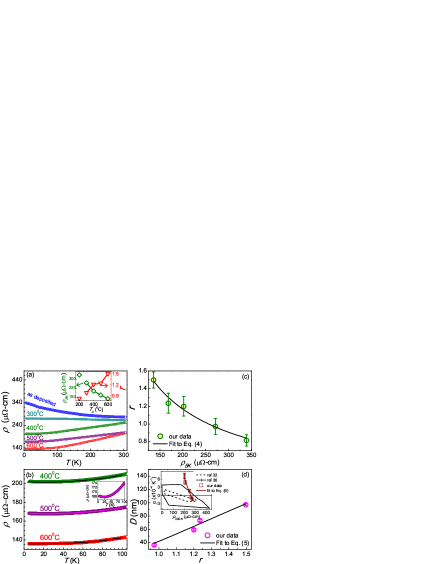
Now we describe the electrical transport in these PLD grown CMS films. Figure 4(a) shows the temperature dependence of longitudinal () in zero field for the as-deposited films as well as for those annealed at 300, 400, 500, and 600∘C. In the as-deposited state, the temperature coefficient () of resistivity is negative in the temperature range 5 K to 300 K with a residual resistivity ratio [] of 0.8. This behavior is very unlike of a normal metal. The metallic nature of the films improves on annealing and a value of 1.5 is achieved after the heat treatment at 600∘C, which is comparable with earlier reported values of for CMS films.Raphael The enhancement of with the is a result of the improvement in crystallographic ordering and, hence, a reduction of defect concentration in the film. The dependence of and at 5 K with are shown in the inset of Fig. 4(a). These data reveal that a distinctly metallic transport sets in only after annealing at 300∘C. In the case of disordered metals the resistivity becomes temperature independent when the elastic mean free path approaches the interatomic distances. This sets a limit on 150-cm, the so-called Mooji criterion,Mooij often satisfied by metallic glasses, although large deviations are seen which suggests non-universality of this criterion. The resistivity of these films derives contributions from (i) the massive atomic disorder almost to the limit of being amorphous in as-grown films, (ii) transparency of grain boundaries whose number density decreases with increasing , and (iii) the presence of antisite disorder. We believe that the huge changes in resistivity after annealing are primarily due to crystalline nature of the films and concomitant disorder at the large number of grain boundaries. We have examined our data using the grain boundary model proposed by Reiss et al.,Reiss which can be viewed as a quantum correction to the classical Drude conductivity. This model attributes the reduced conductivity of the granular media to the number density and quantum transparency of grain boundaries crossed by an electron during two successive scattering events. In such scenario the effective mean free path is expressed as:
| (2) |
where is the mean free path in the absence of granularity, is the transmission probability of the electrons through the grain boundary, and is the grain size. The resistivity is thus written as:Nigro
| (3) |
where = -ln, = , = . The quantities , , and are the mass, Fermi velocity, and density of conduction electrons, respectively. From Eq. (3), we can easily write the following relation:
| (4) |
where . In Fig. 4(c), the values of for different films are reported as a function of along with the fitting of the data by using Eq. (4) with and -cm are well compared to the values obtained for single crystal CMS.Lance A high value of intra-grain room temperature resistivity -cm compares in any case fairly well with the values reported in the literature.Kartik We can also find a relation between and from Eq. (3) as follows:
| (5) |
Figure 4(d) shows the fit of the experimental data by the above expression, which gives the value of =(7.060.8) 10-5 -cm2. Since we have = (3.550.62)10-4 -cm2 for our CMS films, we get and hence a fairly strong coupling between the grains comes out even though the films have negative thermal coefficient of resistivity (TCR). The TCR is defined as , which can be written as:Nigro
| (6) |
where .
The calculated by fitting the data with Eq. (6), gives = (96.14.8)-cm and (300K)= (25.73.2). Our values of for different films agree fairly well with the MooijMooij and TsueiTsuei criterion.
Now, we move to discuss the resistivity of films which have positive TCR (). The of a ferromagnetic metal film derives contributions from the defects, which is temperature independent, as well as from electron-electron scattering (e-e), one magnon scattering (1MS) and weak localization (WL) effects in the disordered phase. The below can thus be expressed as
| (7) |
where the coefficients , and corresponds to e-e, 1MS and WL processes. Here, we have ignored the -linear electron-phonon scattering term, which is expected to dominate only for . Generally, for half-metallic systems, the 1MS process is not possible due to absence of spin down states at . However, at finite temperature, the spin fluctuations in the minority bands can make a non-zero contribution to 1MS scattering. Furukawa has proposed that an unconventional 1MS can be possible, which leads to dependence of the resistivity.Furukawa The term in Eq. (7) emulates a low temperature upturn seen in of 400 and 500∘C annealed film. The possible origin of this upturn is the weak localization due to e-e interaction effects, probably coming from the presence of impurities/disorder, or their combined effect with lattice dynamics. We found this upturn near 25 K for 500∘C annealed film as shown in the inset of Fig. 4(b) and this minimum is not affected by the application of external magnetic field up to 0.3 T which negates the possibility of the well known Kondo-effect. A similar upturn in resistivity has been reported for Heusler alloys such as Ni2MnGe,Lund CMSSingh1 ; Geiersbacha and Co2MnxTi1-xAl.Aftab To understand the effect of different scattering processes, we have fitted the resistivity curves below 100 K by using Eq. (7) and the fitting parameters are summarized in Table I with the error in second decimal place. From these parameters, one can find the relative weights of the respective resistivity components. The dominance of e-e scattering process is likely due to grain boundaries and dominates up to 35 K. At very low temperature, the magnetic scattering of quasiparticles is very small or nearly zero. Hence only e-e scattering would contribute to the resistivity the most. But, at some higher temperature the spin fluctuations near modify the electronic band structure and this may lead to 1MS scattering. The different behaviour of curves and large variation in residual and room temperature resistivities and in thin films as compared to those for bulk samplesLance of CMS could also be due to the significant contribution from the interface between the film and the substrate. This shows the importance of investigating the interface effects on the resistivity of these materials for fundamental and industrial point of view.
| ∘C | |||||
|---|---|---|---|---|---|
| 400 | 202.9 | 9.3110-4 | 9.9810-7 | -0.421 | 0.9999 |
| 500 | 169.1 | 7.5110-4 | 9.9710-7 | -0.333 | 0.9999 |
| 600 | 135.8 | 6.3410-5 | 6.0110-6 | 0 | 0.9999 |
III.3.2 Anomalous Hall Effect
The Hall resistivity () in ferromagnetic films provides valuable information about dominant carrier scattering mechanism, spin-orbit scattering, state of magnetization as well as non-trivial spin texture and their stability in H-T phase space. The of an inhomogeneous ferromagnet can be expressed as:
| (8) |
here the first term is the contribution from the Lorentz force experienced by the carriers in the presence of externally imposed magnetic field . In the simple free electron model, , where is the carrier concentration. The values for coefficient are obtained from the slope of data at high field range. The second term is the well known anomalous Hall effect (AHE), which derives contribution from the effect of spontaneous magnetization on scattering and a non-zero band average anomalous velocity transverse to the applied field.Nagaosa The values of for each temperature are obtained by extrapolating the data from the saturation value to zero magnetic field. The phenomenon of AHE has already been established by considering its extrinsic origin based on the skew scatteringLuttinger ; Smit and side jump mechanismsBerger on account of asymmetric scattering of spin-polarized charge carriers in the presence of spin-orbit interaction as well as the intrinsic origin, ascribed to Berry phase of Bloch electrons.Karplus ; Luttinger ; Smit ; Berger ; Berry The anomalous Hall resistivity ( = , is the magnetic moment measured along z direction) scales with the longitudinal resistivity () as , where the exponent varies from 1 to 2 depending on the strength of disorder. The topological Hall resisttivity () evolves with the field, which affects the inhomogeneous spin texture in a non-trivial manner; but reduces to zero at high fields beyond saturation of magnetization.
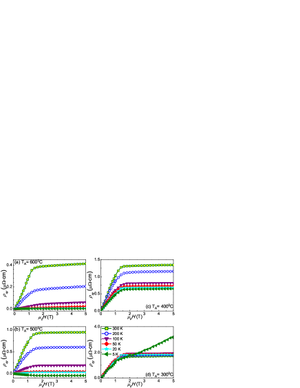
Figure 5 shows data measured at different temperatures for the CMS films. Below saturation, is governed by the AHE and increases with the increase in the sample magnetization. Like , the decreases with decreasing temperature and becomes almost constant below 20 K. The low temperature values of changes with the . For the films annealed at 600∘C, the is close to zero, whereas, in 500∘C annealed film, the gains a negative values due to DO3 disorder and finally, it attains a positive values for 400 and 300∘C annealed samples on account of higher degree of 2 disorder.
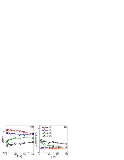
Figure 6(a) shows the carrier concentration () of CMS films as a function of temperature for different values. The Hall mobility () = remains nearly constant as shown in Fig. 6(b). The film annealed at 600∘C is characterized by and of 1.19 1029 m-3 and 0.4 cm, respectively measured at room temperature. Our values of and are comparable to previously reported studies on MgO.Schneider2
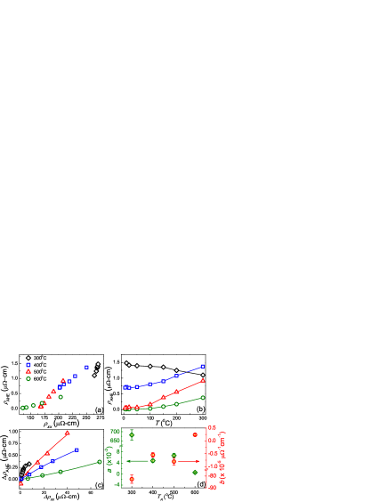
The scaling between and is an important issue for better understanding of AHE. This correlation suggests the presence of dominant scattering mechanisms in both resistivities responsible for the appearance of AHE phenomenon caused by defects and antisite disorder.Vidal In general, we have,
| (9) |
where the coefficients and give the proportions of skew scattering, side-jump and the intrinsic mechanisms. Figure 7(a) shows the variation of with for various films, whereas, the temperature dependence of is shown in Fig. 7(b). This also follows as the behaviour with respect to temperature as for . So can be separated into temperature-independent [] and temperature-dependent [] resistivity below 20 K. Hence, Eq. (9) can be rewrittten as:
| (10) |
where is the residual anomalous Hall resistivity. By substracting values at two different temperatures, we can separate the temperature dependent part. Hence, Eq. (10) will be reformed as:
| (11) |
Here we have taken the difference in the resistivities with respect to the values at 20 K and plotted in Fig. 7(c) with fitting in according to Eq. (11). We find a linear dependence for all the films with different slopes except for 300∘C annealed films. The slopes of the lines decrease with increase in as the skew scattering term () decreases where as the scattering independent term () increases as shown in Fig. 7(d). These two fitting parameters decide the dominance of the scattering present in the films. The values for and are (61) and (2.390.26) -1cm-1, respectively for 21 ordered 600∘C annealed film and we found with 135.8 -cm. This clearly suggests the dominance of linear scaling due to skew-scattering mechanism. The values of these fitting parameters change very drastically as we change . So the structural ordering as well as magnetization in addition to other factors like impurities in the films and their thermal history are the important constituents which affect the scattering mechanism in the films.
III.3.3 Topological Hall Effect
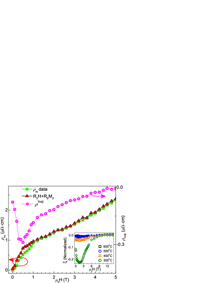
Now we discuss the THE, which emerges due to inhomogeneous spin textures in the presence of magnetic field, but reduces to zero at very high field. The film annealed at 300∘C may show a non trivial spin character as it contains sufficient amount of antisite disorder as well as smaller grain size, which can lead to inhomogeneous magnetization. The canting of the magnetic spins makes the magnetization of the 300∘C annealed films depart from in-plane easy axis. The possibility of minority spins at also allows the scattering between spin-up and spin-down carriers. Hence, the spin canting and presence of minority spins at may show some signatures of THE in 300∘C annealed films at low temperature. The can be obtained by subtracting the () from . The experimental data measured at 5 K for 300∘C annealed film along with the calculated () values and , are shown in Fig. 8. The and () increase monotonically with and coincide at high magnetic fields suggesting a diminishing effect of . The contribution of shows a minima around 0.5 T. This type of behaviour has been observed in previous experimentsKanazawa ; Neubauer ; Lee and described in theories.Yi The inset of Fig. 8 shows a systematic variation of normalized topological Hall resistivity [=] for differently annealed films to understand the effect of disorder on . The films annealed at 500 and 600∘C do not show any THE due to strong magnetic coupling, robust uniaxial in-plane anisotropy, and a half-metallic character. As the reduced to 300∘C, a minimum in the occurs. This observation shows that the inhomogeneous magnetization which contribute to diminishes as the films become more ordered.
III.3.4 Anisotropic magnetoresistance
Ferromagnetic materials show a distinct contribution that depends on the direction of magnetization with respect to the direction of the current used to measure . This effect, commonly known as Anisotropic magnetoresistance (AMR), arises from spin-orbit interaction and is of significant technological and fundamental interest. The AMR is defined as;
| (12) |
where represents the resistivity when the current flows parallel (perpendicular) to the magnetization. The original work of Cambell et al. attributes AMR to s-d scattering from the conduction states and successfully explains the AMR data of crystalline 3d transition metal alloys.Campbell A further improvement of the theory by Malozemoff takes into account the s-s scattering as well,Malozemoff but these models do not consider the spin polarization of s-states. Kokado et al. have shown that when the dominant s-d scattering process occurs between those states which have same type of spin, the AMR ratio is negative (), and when the dominant scattering occurs between opposite spin states, the sign tends to be positive.Kokado This prediction has a special significance for the half-metallic systems as they have only one type of spin states at , and hence, should show a predominantly negative AMR. We have measured the AMR of our films in a field strength of 0.3 T, which is sufficient to saturate the magnetization.
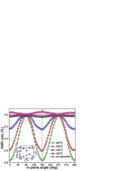
Figure 9 shows the dependence of the AMR ratio on the angle between the current and external field for CMS films measured at 7 K, where the AMR ratio is defined as [], where corresponds to . The obtained values of AMR ratios are comparable with the earlier reports on mangnites Ziese ; Favre and full-Heusler alloy Co2FexMn1-xSi.Yang Our data show a twofold symmetry for all the films with minimum occurring at = 0∘ and 180∘, showing negative AMR values. The magnitude of the AMR increases with the (see the inset of Fig. 9) and changes its sign for highly disordered as-deposited film suggesting changes in the DOS at and the degree of spin polarization due to increasing structural disorder. These observation indicates that even though the film annealed at 400∘C exhibits half-metallic character with ordering, there must be some overlap between and the minority band which decreases further on raising the due to improvement of structural ordering.
IV CONCLUSIONS
In summary, we prepared laser ablated thin films of Co2MnSi with different degree of disorder realized by post-deposition annealing in the temperature range of 300 to 600∘C. In the as-deposited state, the film is composed of nano-crystalline grains with 2 type disorder. The film behaves as a strongly disordered metal with negative TCR due to the scattering from grain boundaries and the site disorders within the grains. Annealing improves structural ordering from disordered nanocrystalline to 2 phase and finally highly ordered 21 phase is obtained at 600∘C. The system becomes metallic with positive TCR for 300∘C. The saturation magnetization builds up on annealing and reaches the bulk value as predicted by Slater-Pauling rule at = 600∘C. The behaviour of TCR, room temperature resistivity and residual resistivity ratio are analyzed in the framework of a model based on quantum transparency of grain boundaries. These results establish three structural states in our films, the as-prepared nanocrystalline phase with strong site disorder, an intermediate phase with a small amount of site order inside the grains, and the crystalline phase with long-range structural order. A systematic study of anomalous Hall effect reveals the experimental evidence of skew-scattering phenomena. We also observed an overtone of topological Hall effect in our strongly disordered nano-crystalline 300∘C annealed films which vanishes at higher magnetic fields. The normalized value of topological Hall resistivity () is almost zero for 500 and 600∘C annealed films. We found a maximum value of 0.22 for 300∘C annealed film. The annealing temperature dependence of the THE suggests the canting and/or texturing of spins in the films annealed at 300∘C. An AMR ratio of -0.76% is obtained for 600∘C annealed film, which decreases sharply as reduces, whereas, we found AMR of 0.04 for as-deposited film. This small positive value of AMR suggests disappearance of half-metallicity.
V ACKNOWLEDGEMENT
This research has been supported by Council for Scientific and Industrial Research (CSIR), Government of India. H.P. would like to thank V. P. S. Awana for directing him to use the PPMS. He also thanks the DST Unit on Nanosciences (IIT Kanpur) for the SEM and GIXR measurements and acknowledges financial support from Indian Institute of Technology Kanpur and CSIR. R.C.B. acknowledges J. C. Bose Fellowship of the Department of Science and Technology, Govt. of India.
References
- (1) R. Kainuma, Y. Imano, W. Ito, H. Morito, S. Okamoto, O. Kitakami, K. Oikawa, A. Fujita, T. Kanomata, and K. Ishida , Nature 439, 957 (2006).
- (2) T. Krenke, E. Duman, M. Acet, E. F. Wassermann, X. Moya, L. Mañosa, and A. Planes, Nat. Mat. 4, 450 (2005).
- (3) P. G. van Engen, K. H. J. Bushow, R. Jongebreuer, and M. Erman, Appl. Phys. Lett. 42, 202 (1983).
- (4) S. Bosu, Y. Sakuraba, K. Uchida, K. Saito, T. Ota, E. Saitoh, and K. Takanashi, Phys. Rev. B 83, 224401 (2011).
- (5) J. H. Wernick, G. W. Hull, T. H. Geballe, J. E. Bernadini, and J. V. Waszczak, Mater. Lett. 2, 90 (1983).
- (6) S. Chadov, X. Qi, J. Kübler, G. H. Fecher, C. Felser, and S. C. Zhang, Nat. Mat. 9, 541 (2010).
- (7) H. Lin, L. A. Wray, Y. Xia, S. Xu, S. Jia, R. J. Cava, A. Bansil, and M. Z. Hasan, Nat. Mat. 9, 546 (2010).
- (8) H. A. Kierstead, B. D. Dunlap, S. K. Malik, A. M. Umarji, and G. K. Shenoy, Phys. Rev. B 32, 135 (1985).
- (9) J. H. Park, E. Vescovo, E. Kim, C. Kwon, R. Ramesh, and T. Venkatesan, Nature 392, 794 (1998).
- (10) Y. Ji, G. J. Strijkers, F. Y. Yang, C. L. Chien, J. M. Beyers, A. Anguclouch, G. Xiao, and A. Gupta, Phys. Rev. Lett. 86, 5585 (2001).
- (11) D. Ristoiu, J. P. Nozières, C. N. Borca, B. Borca, and P. A. Dowben, Appl. Phys. Lett. 76, 2349 (2000).
- (12) M. C. Kautzky, F. B. Mancoff, J. F. Bobo, P. R. Johnson, R. L. White, and B. M. Clemens, J. Appl. Phys. 81, 4026 (1997).
- (13) S. Fujii, S. Sugimura, Ishida, and S. Asano, J. Phys: Con. mat. 2, 8583 (1990).
- (14) M. Zander, J. Herfort, K. Kumakura, H-P Scöhnherr, and A. Trampert, J. Phys. D: Appl. Phys. 43, 305004 (2010).
- (15) K. Kasahara, K. Yamamoto, S. Yamada, T. Murakami, K. Hamaya, K. Mibu, and M. Miyao, J. Appl. Phys. 107, 09B105 (2010).
- (16) W. H. Wang, M. Przybylski, W. Kuch, L. I. Chelaru, J. Wang, Y. F. Lu, J. Barthel, H. L. Meyerheim, and J. Kirschner, Phys. Rev. B 71, 144416 (2005).
- (17) L. J. Singh, Z. H. Barber, Y. Miyoshi, Y. Bugoslavsky, W. R. Branford, and L. F. Cohen, Appl. Phys. Lett. 84, 2367 (2004).
- (18) H. Schneider, G. Jakob, M. Kallmayer, H. J. Elmers, M. Cinchetti, B. Balke, S. Wurmehl, C. Felser, M. Aeschlimann, and H. Adrian, Phys. Rev. B 74, 174426 (2006).
- (19) H. Pandey, P. C. Joshi, R. P. Pant, R. Prasad, S. Auluck, and R. C. Budhani, J. Appl. Phys. 111, 023912 (2012).
- (20) H. Schneider, E. Vilanova, B. Balke, C. Felser, and G. Jakob, J. Phys. D Appl. Phys. 42, 084012 (2009).
- (21) Anupam, P. C. Joshi, P. K. Rout, Z. Hossain and R. C. Budhani, J. Phys. D: Appl. Phys. 43, 255002 (2010).
- (22) V. Toutam, H. Pandey, S. Singh, and R. C. Budhani, AIP ADVANCES 3, 022124 (2013).
- (23) P. K. Rout, H. Pandey, Anupam, P. C. Joshi, Z. Hossain, and R. C. Budhani, manuscript submitted.
- (24) U. Geiersbach, A. Bergmann, and K. Westerholt, J. Mag. Mag. Mat. 240, 546 (2002).
- (25) M. P. Raphael, B. Ravel, Q. Huang, M. A. Willard, S. F. Cheng, B. N. Das, R. M. Stroud, K. M. Bussmann, J. H. Claassen, and V. G. Harris, Phys. Rev. B 66, 104429 (2002).
- (26) S. Kämmerer, A. Thomas, A. Hütten, and G. Reiss, Appl. Phys. Lett. 85, 79 (2003).
- (27) K. Kim, S. J. Kwon, and T. W. Kim, Phys. Status Solidi B Basic Res. 241, 1557 (2004).
- (28) T. Ambrose, J. J. Krebs, and G. A. Prinz, Appl. Phys. Lett. 76, 3280 (2000).
- (29) H. C. Kandpal, G. H. Fecher, C. Felser, and G. Schönhense, Phys. Rev. B 73, 094422 (2006).
- (30) Y. V. Kudryavtsev, V. N. Uvarov, V. A. Oksenenko, Y. P. Lee, J. B. Kim, Y. H. Hyun, K. W. Kim, J. Y. Rhee, and J. Dubowik, Phys. Rev. B 77, 195104 (2008).
- (31) P. J. Webster, J. Phys. Chem. Solids 32, 1221 (1971); K. R. A. Ziebeck and P. J. Webster, J. Phys. Chem. Solids 35, 1 (1974).
- (32) Y. Takamura, R. Nakane, and S. Sugahara, J. Appl. Phys. 105, 07B109 (2009).
- (33) I. Galanakis, P. H. Dederichs, and N. Papanikolaou, Phys. Rev. B 66, 174429 (2002).
- (34) J. H. Mooij, Phys. Status Solidi A 17, 521 (1973).
- (35) G. Reiss, J. Vancea, and H. Hoffmann, Phys. Rev. Lett. 56, 2100 (1986).
- (36) A. Nigro, G. Nobile, M. G. Rubino, and R. Vaglio, Phys. Rev. B 37, 3970 (1988).
- (37) K. Senapati, N. K. Pandey, Rupali Nagar, and R. C. Budhani, Phys. Rev. B 74, 104514 (2006).
- (38) C. C. Tsuei, Phys. Rev. Lett. 57, 1943 (1986).
- (39) N. Furukawa, J. Phys. Soc. Jpn. 69, 1954 (2000).
- (40) M. S. Lund, J. W. Dong, J. Lu, X. Y. Dong, C. J. Palmstrm, and C. Leighton, Appl. Phys. Lett. 80, 4798 (2002).
- (41) L. J. Singh, Z. H. Barber, Y. Miyoshi, W. R. Branford, and L. F. Cohen, J. Appl. Phys. 95, 7231 (2004).
- (42) M. Aftab, G. H. Jaffari, S. K. Hasanain, T. A. Abbas, and S. I. Shah, J. Phys. D: Appl. Phys. 45, 475001 (2012).
- (43) L. Ritchie, G. Xiao, Y. Ji, T. Y. Chen, C. L. Chien, M. Zhang, J. Chen, Z. Liu, G. Wu, and X. X. Zhang, Phys. Rev. B 68, 104430 (2003).
- (44) N. Nagaosa, J. Sinova, S. Onoda, A. H. MacDonald, and N. P. Ong, Rev. Mod. Phys. 82, 1539 (2010).
- (45) J. M. Luttinger and W. Kohn, Phys. Rev. 97, 869 (1955).
- (46) J. Smit, Physica 24, 39 (1958).
- (47) L. Berger, Phys. Rev. B 2, 4559 (1970).
- (48) R. Karplus and J. M. Luttinger, Phys. Rev. 95, 1154 (1954).
- (49) M. V. Berry, Proc. R. Soc. London, Ser. A392, 45 (1984).
- (50) E. V. Vidal, H. Schneider, and G. Jakob, Phys. Rev. B 83, 174410 (2011).
- (51) N. Kanazawa, Y. Onose, T. Arima, D. Okuyama, K. Ohoyama, S. Wakimoto, K. Kakurai, S. Ishiwata, and Y. Tokura, Phys. Rev. Lett. 106, 156603 (2011).
- (52) A. Neubauer, C. Pfleiderer, B. Binz, A. Rosch, R. Ritz, P. G. Niklowitz, and P. Böni, Phys. Rev. Lett. 102, 186602 (2009).
- (53) M. Lee, W. Kang, Y. Onose, Y. Tokura, and N. P. Ong, Phys. Rev. Lett. 102, 186601 (2009).
- (54) S. D. Yi, S. Onoda, N. Nagaosa, and J. H. Han, Phys. Rev. B 80, 054416 (2009).
- (55) I. A. Campbell, A. Fert, and O. Jaoul, J. Phys. C: Solid State Phys. 3 (Metal Phys. Suppl.) S95 (1970).
- (56) A. P. Malozemoff, Phys. Rev. B 32, 6080 (1985).
- (57) S. Kokado, M. Tsunoda, K. Harigaya, and A. Sakuma, J. Phys. Soc. Jpn. 81, 024705 (2012).
- (58) M. Ziese, Phys. Rev. B 62, 1044 (2000); M. Ziese and S. P. Sena, J. Phys. Con. Mat. 10, 2727 (1998).
- (59) E. Favre-Nicolin and L. Ranno, J. Magn. Magn. Mater. 272, 1814 (2004).
- (60) F. J. Yang, Y. Sakuraba, S. Kokado, Y. Kota, A. Sakuma, and K. Takanashi, Phys. Rev. B 86, 020409(R) (2012).