Ab-initio study on the possible doping strategies for MoS2 monolayers
Abstract
Density functional theory is used to systematically study the electronic and magnetic properties of doped MoS2 monolayers, where the dopants are incorporated both via S/Mo substitution or as adsorbates. Among the possible substitutional dopants at the Mo site, Nb is identified as suitable p-type dopant, while Re is the donor with the lowest activation energy. When dopants are simply adsorbed on a monolayer we find that alkali metals shift the Fermi energy into the MoS2 conduction band, making the system n-type. Finally, the adsorption of charged molecules is considered, mimicking an ionic liquid environment. We find that molecules adsorption can lead to both n- and p-type conductivity, depending on the charge polarity of the adsorbed species.
I Introduction
In recent years two dimensional (2D) materials have attracted a growing interest due to their potential for future nano-electronics applications, owing to their unusual physical, optical and electrical properties arising from the quantum confinement associated to their ultra thin structure RPP_2011_74 . These considerations apply particularly well to layered transition metal di-chalcogenides (LTMDs) in which a multitude of electronic states have been observed, namely metallicity, semi-conductivity and charge density waves. Given the richness in the electronic properties it is not a surprise that this materials class has been called out as the ideal platform for a multitude of applications Adv_1969_18 ; Adv_1987_36 . For example, the prototypical LTMD, molybdenum di-sulfide MoS2, has been widely explored as lubricant Wear_1967_10 , catalyst CatT_2005_107 and as lithium ion battery anode ChAJ_2012_7 .
Structurally MoS2 consists of covalently bonded S-Mo-S 2D hexagonal planes (monolayers), which in the bulk are bound together in a layered structure by weak van der Waals forces JPCM_2000_12 . Interestingly, the electronic properties of bulk MoS2 show a strong dependence on the layer thickness NL_2010_10_1271 . Single MoS2 monolayers are particularly intriguing. These display a direct band-gap of 1.9 eV, which makes them a semiconducting alternative to gapless graphene. Indeed the band-gap of graphene can be opened by fabricating nanoribbons PRL_2008_100_206803 or by depositing it over a suitable substrate Nature_2007_6_770 . However this comes at the cost of deteriorating the carrier mobility due to edge and impurity scattering PNAS_2007_104_18392 . In contrast, the absence of dangling bonds, the high crystallinity, and the low dimensionality, make the performance of LTMDs comparable to those of currently existing Si transistors at the scaling limit JAP_2007_101 ; IEEE_2011_58 ; NL_2012_12_1538 . MoS2 monolayer based transistors have been recently demonstrated to operate at room temperature, with a mobility of at least 200 cm2/Vs and on/off current ratios of 108 with low standby power dissipation Nature_2011_6 . Interestingly, both n-type Nature_2011_6 ; PRL_2010_105 ; Adv_2012_24_2320 ; Small_2012_8_682 and p-type ACIEd_2011_50_11093 ; Small_2012_8_966 conductivities have been reported for ultra-thin MoS2 layers, depending on the experimental details. The origin of such diverse conducting properties remains to date far from being clear.
The possible creation of Mo and/or S vacancies in MoS2 monolayers during the growth cannot be used as a doping strategy, since those vacancies always produce deep trap states in the MoS2 monolayer band-gap PRL_2004_92 . In a recent study we have investigated how unintentional doping of the substrate holding a MoS2 monolayer may determine its conductivity arXiv:1301.2491 . Here we explore possible strategies for doping directly into the MoS2 monolayer. Although there are studies available on specific dopants for single layer MoS2 PRL_2004_92 ; APL_2010_96_082504 ; JPChC_2011_115_13303 , to our knowledge there is not yet a systematic investigation comparing the doping properties of the various defects, when they are incorporated in either a substitutional position or they are adsorbed on the surface. Moreover, it has been reported that in a liquid-gated electric double layer transistor, the ions can modulate the electronic properties from insulating to metallic through electrostatic induced carrier doping in the transport channel at a finite gate bias NL_2012_12_2988 . Compared with other dopants, such as metals and light atoms, ionic liquids have several advantages as surface dopants: a large variety of such ionic complexes are available, they can accumulate more carriers than conventional solid state gated transistors, and they do not induce structural disorder like substitutional dopants. In fact, ambipolar transistor operation has been achieved using thin flakes of MoS2 in an ionic liquid gated environment NL_2012_12_1136 . The present work explores also this possibility.
Here we systematically study the effects of dopants on the electronic structure of a MoS2 monolayer, by calculating the formation energies and the electronic properties of halogens, non-metals, transition metals and alkali metals added in various geometrical configurations. Our aim is that of identifying potential candidates for making MoS2 monolayers either n- or p-type in a controlled way. Then we present an investigation of the electronic structure of MoS2 monolayers when two molecular ions, NH and BF, are adsorbed at the surface. The paper is organized as follows. After a brief discussion of the computational methods used we turn our attention to the case of substitutional doping by looking at both at the S and the Mo site. Next we consider the case of doping by adsorption of alkali and molecular ions. At the end of the results section we briefly discuss the robustness of our calculations against the particular choice of exchange and correlation functional and finally we conclude.
II Methodology
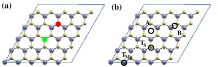
In order to investigate the electronic properties of a MoS2 monolayer doped with impurities, ab-initio calculations are performed using density functional theory PRB_1964_136 ; PRA_1965_140 within the local spin density approximation (DFT-LSDA) for the exchange and correlation potential. In particular we consider the Ceperly-Alder LSDA parametrization PRL_1980_45 as implemented in the SIESTA code IOP_2002_14 . In our calculations double- polarized PRB_2001_64 numerical atomic orbitals basis sets are used for all atoms, and the Troullier-Martins scheme is used for constructing norm-conserving pseudopotentials PRB_1991_43 . A 55 hexagonal supercell [see Fig. 1(a)] with (15.6615.66) Å2 lateral dimensions is constructed and doping is introduced by replacing/adding a single atom in the supercell. This corresponds to simulating a Mo1-xAxS2-yBy periodic system with () when the doping is at the Mo (S) site. An equivalent plane wave cutoff of 250 Ry is used for the real space mesh and the Brillouin zone is sampled over a 551 Monkhorst-Pack -grid. Periodic boundary conditions are applied and a vacuum layer of at least 15 Å is placed above the monolayer to minimize the interaction between the adjacent periodic images. A temperature of 300 K is used when populating the electronic states with a Fermi distribution. The relaxed geometries are obtained by conjugate gradient, where all the atoms in the supercell are allowed to relax until any force is smaller than 0.02 eV/Å.
In order to verify that the calculated impurity level alignments are robust against the choice of exchange correlation functional, we repeat the calculations for the main results by using the screened hybrid functional of Heyd-Scuseria-Ernzerhof (HSE06) HSE . All DFT calculations based on the HSE06 functional are carried out with the projector augmented wave (PAW) pseudo potential plane-wave methodPRB_1994_50_17953 as implemented in the VASP code PRB_1996_54_11169 . A 331 Monkhorst-PackPRB_1976_13_5188 -point grid is employed and the plane wave energy cutoff is 500 eV.
The formation energy of a particular substitutional dopant, , is defined as
| (1) |
where (MoS+X) is the total energy of the system including the substitutional atom X, (MoS2) is the total energy of the corresponding pristine MoS2 monolayer, while (X) and (host) are respectively the energies of the substitutional atom X and of the substituted Mo (S) host atom in their bulk (diatomic molecule) forms. In contrast the formation energy for an adsorbate, , can be written as
| (2) |
where (MoS2+Y) refers to the total energy when the adsorbate Y is attached to MoS2, and (Y) is the energy of an adsorbate Y in its bulk form. In order to find the most stable configuration for adsorption, we consider four possible positions labeled as follows: TS (adsorbate on top of S), TMo (adsorbate on top of Mo), A (adsorbate above the center of the hexagonal ring of MoS2), and B (adsorbate above the middle of the Mo-S bond) [see Fig. 1(b)].
III Results and discussion
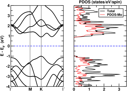
Before discussing the formation energy and the electronic structure of the possible dopants let us here briefly review the electronic properties of a single MoS2 monolayer. As the MoS2 thickness is decreased from bulk to a few layers, the valence band minimum shifts from half way along -K line towards K NL_2010_10_1271 . For a monolayer the band-gap becomes direct at K (see Fig. 2), a transition which has been recently observed experimentally NL_2010_10_1271 . The computed LSDA band-gap of 1.86 eV is in good agreement with the experimental optical band-gap of 1.90 eV PRL_2010_105 , although such an agreement has to be considered fortuitous. In fact the absorption edge of an optical excitation measures the energy difference between the quasi-particle band-gap and the exciton binding energy. In MoS2 monolayers this latter is of the order of 1 eV, as confirmed recently by many-body calculations Ramasubramaniam . Thus, one expects that the true quasi-particle spectrum has a band-gap of approximately 2.9 eV, in good agreement with that computed with the scheme, either at the first order level Ramasubramaniam (2.82 eV) or self-consistently Lamb (2.76 eV). At the end of this section we will discuss how band-gap corrections, via the HSE06 functional, affect our main results. In any case, for both bulk and monolayer the band-structure around the band-gap is derived mainly from Mo-4 orbitals (see the orbital projected density of state, PDOS, in Fig. 2), although there are also small contributions in the valence band from the S-3 ones.
| Impurity | (/impurity) | Eform(eV) |
|---|---|---|
| F, Cl, Br | 1.00 | 0.60 (F), 1.93 (Cl), 2.16 (Br) |
| I | 0.00 | 2.53 |
| N, P | 1.00 | 2.90 (N), 1.89 (P) |
| As | 0.00 | 1.91 |
| Re | 1.00 | 2.05 |
| Ru | 2.00 | 3.05 |
| Rh | 3.00 | 4.15 |
| Pd | 4.00 | 5.63 |
| Ag | 2.57 | 7.28 |
| Cd | 1.58 | 6.11 |
| Nb, Zr, Y | 0.00 | -0.19 (Nb), -0.48 (Zr), 0.52 (Y) |
III.1 Substitutional doping
Substitution at the S site
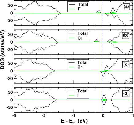
We begin our analysis by substituting a surface S atom with elements taken from the halogen family, namely F, Cl, Br and I. These are expected to act as a source of n-type doping for MoS2, since they have one additional electron with respect to S. The DOSs for the supercell including one atom of the halogen family are presented in Fig. 3. As a representative system, we discuss in details results for Cl-doping, since the other halogens present a similar electronic structure. A Cl-doped MoS2 monolayer has a magnetic ground state, where an occupied defect level is formed at about 0.4 eV below the conduction band minimum (CBM). The corresponding minority state is located above the CBM and is empty. These defect levels originate from the hybridization between the Cl-3 and the Mo-4 states. Similarly to the Cl substitution, for both F and Br dopants (isoelectronic to Cl) the system is para-magnetic, having a magnetic moment of approximately 1 . In the case of F substituting S, the spin-splitting is larger than that of Cl, whereas it is smaller for the Br substitutional case. Eventually, when S is replaced by iodine, the impurity becomes nonmagnetic, although the impurity level is still located well below (0.3 eV) the CBM [see Fig. 3(d)]. Note that having an impurity presenting a ground state with finite magnetic moment has nothing to do with diluted ferromagnetism in -type systems, as sometimes erroneously claimed in literature. This simply indicates that the additional electron remains unpaired and localized around the impurity Andrea . The dependence of the spin-splitting of the impurity level on the atomic number simply follows the well-known trend for the exchange-correlation integral Janak .
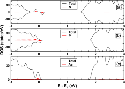
We then investigate the possibility of p-type doping obtained by replacing a S atom with a group V element of the periodic table, namely N, P and As (see Fig. 4). In the case of N the supercell has a magnetic ground state [see Fig. 4(a)], with a magnetic moment of 1 and a spin-splitting of about 0.20 eV. In both the spin channels gap states are introduced above the valence band maximum (VBM), and these are formed by hybridization between the N-2 and the Mo-4 valence orbitals. Similarly, when substituting S with P, the system is again magnetic, but the defect states are rigidly shifted closer to the VBM of the pristine MoS2 monolayer in both the spin channels. The spin-splitting remains similar to that of N. Finally for the As substitutional case, the defect states shift even more towards the VBM. Additionally, the spin-splitting vanishes and the system becomes a p-type semiconductor. The partially unoccupied impurity band however shows very little dispersion and it is separated from the valence band by about 0.08 eV. Such an impurity band is formed mainly by As-4 and Mo-4 orbitals.
To summarize our results for S substituting impurities, we find that most dopants create localized, spin-polarized, gap states. When increasing the dopant atomic number the spin-splitting reduces and the states move towards the VBM/CBM. Among the many dopants investigated As appears to give the most promising DOS for p-type doping, since the associated diamagnetic impurity band is very close to the VBM. In the case of n-type doping, all substituent dopants have donor states located rather far from the MoS2 CBM and therefore they are rather localized. In addition to these considerations a look at Table 1, where we present the formation energy of the various dopants, reveals that all the S substituents possess a rather large formation energy, i.e. they are unlikely to form under equilibrium thermodynamical conditions. The only viable formation channel is offered by filling S vacancies, which have been recently demonstrated to form with relatively ease PRL_2012_109_035503 . Therefore, it appears that a strategy for doping at the S site may be that of growing S poor samples and then of filling the vacancies with an appropriate donor/acceptor sulfur replacement.
Substitution at the Mo site
Next we consider substitutional doping at the Mo site with different transition metal atoms having a growing number of electrons in the shell. Specifically we consider all the 4 elements in the periodic table ranging from Y to Cd with the only exception of radioactive Tc, which is replaced by Re (5). In general we find that for all the substitutional atoms having a occupancy larger than Mo, the ground state is spin-polarized, while Y, Zr and Nb have a diamagnetic ground state (see Table 1).
Let us again discuss the case of n-type doping first. When Re replaces Mo, one extra electron is added to the supercell. This remains unpaired and occupies a majority spins gap state [Fig. 5(a)], located 0.3 eV below the CBM, with the Fermi energy, located between such state and the CBM. As a consequence the supercell has a magnetic moment of 1 and the DOS for this situation resembles that of Cl substituting S [Fig. 3(b)]. If one forces a non-spin-polarized solution for Re-doped MoS2 monolayer, the donor level is created at about 0.2 eV below the CBM. However, the magnetic ground state is lower in energy than the non-magnetic one by 82 meV/supercell, i.e. a diamagnetic solution is not stable. Note that our non-spin-polarized result is consistent to that reported for similar a calculation ChemAsianJ_2008_3 , where a Re donor level at 0.19 eV below the CBM suggested that Re could be used as n-type dopant in MoS2 nanotubes. Such result thus seems to be robust against spin polarization (the spin polarized impurity state is at 0.3 eV below the VBM). Note that single crystals Re-doped MoS2 have been grown in the past by chemical vapor deposition JCGrow_1999_205_543 .
When one then looks at other transition metal dopants having a -orbitals occupancy larger than Re, an increasing number of gap states is formed. These are progressively occupied so that the excess electrons do not spill into the MoS2 conduction band (see Fig. 5). As a consequence the Fermi energy always lies in the MoS2 band-gap, and in fact it moves deeper into the band-gap as the shell filling of the dopant increases. The excess electrons first fill up the majority spin states of the host -orbitals, until the magnetic moment of the impurity reaches the largest value of 4 for Pd. Then the magnetic moment decreases for Ag and Cd as the additional electrons start to populate the minority spins states (see Table 1).
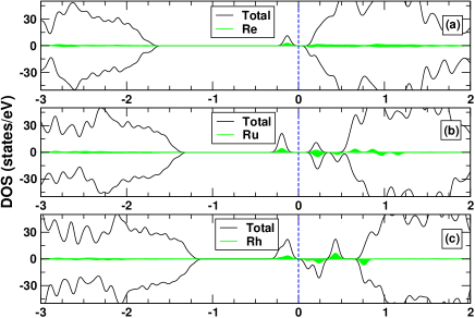
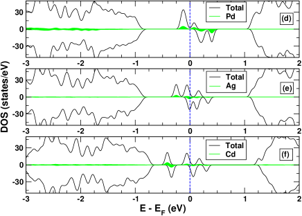
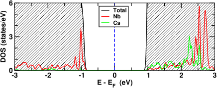
Next we move to study the possibility of obtaining p-type doping by replacing Mo with Nb, Zr and Y, which have respectively one, two and three electrons less than Mo. The case of Nb seems to be particularly attractive. The inclusion of Nb into MoS2 changes little the bond lengths and also the main DOS. The only notable effect is the shift of the Fermi energy below the VBM due to the one electron removal [see Fig. 6(a)]. The newly created defect states are rather delocalized and the charge excess spreads out up to the third nearest neighbor Mo atoms. The states around the VBM mainly originate from hybridized orbitals of Nb and Mo. The valence band now looks sufficiently dispersive in our DFT band-structure, and therefore the mobility is expected to be rather large. Importantly the formation energy for Nb-doping is -0.19 eV, in good agreement with the formation energy of -0.21 eV PRB_2008_78_134104 , obtained theoretically for Nb in bulk MoS2. Overall our results suggest that Nb may be a promising candidate as p-type dopant in MoS2 monolayers. Note that an experimental study JACS_2007_129_12549 shows that Nb-substituted (concentration range 15-25 %) MoS2 nanoparticles can be synthesized, and that they also exhibit p-type character. Finally, for all the other two p-type dopants considered (Y and Zr) the ground state is also non-magnetic (see Table 1). However, in contrast to Nb doping, the defect state becomes less hybridized with the VBM and produces split off acceptor-levels above the VBM for both Zr and Y [see Fig. 6(b) and (c)].
We conclude this section by evaluating the pairing energy between two Nb atoms placed in a 66 supercell. In Table 2 we list the energy difference between the configuration where the two impurities are placed at nearest neighbor positions and when they are placed as far as possible in the supercell. The result suggests that in case of Nb pairs the dopants tend to stay close to each other in the MoS2 monolayer ( 0). Thus, based solely on the pairing energy, Nb dopants would form clusters. Clustering however is likely to be inhibited in by the large energy barrier for Nb diffusion in the MoS2 plane.
| Atom-Atom | (meV) |
|---|---|
| Nb-Nb | -157 |
| Cs-Cs | 166 |
| Nb-Cs | -218 |
Summarizing the situation for transition metal doping at the Mo site we find that, when the dopant has more electrons than Mo, donor states are created deep inside the MoS2 band-gap (at least 0.2 eV below the CBM), with Re being the dopant with the smallest activation energy. However, in all cases the formation energies are large (Table 1). On the contrary, p-type doping obtained by substituting Mo with transition metals such as Nb and Zr creates acceptor states just at the VBM, and the formation energies are also small (Table 1). In fact, for both Nb and Zr, is negative, indicating that substitutional doping will form spontaneously in MoS2 monolayers (note that this is relative to the bulk reference for the dopant). Intriguingly, also for the case of transition metal doping at the Mo site the possibility of filling vacancies remains open. In fact a recent experiment APL_2012_101_102103 has provided evidence for the formation of Mo vacancies in bulk MoS2 via proton irradiation.
III.2 Doping by adsorption
The results of the previous section show that neither Mo substitution with transition metals nor S substitution with non-metal elements appear as promising strategies for obtaining shallow donor states (p-doping is much more promising with Nb). Another possible route for obtaining n-type MoS2 monolayers is by adsorbing H or alkali metals such as Li, K and Cs. This possibility is explored here. Then, in the second part of this section we consider adsorbed molecular ions as potential dopants with both n- and p-type character.
Alkali atom adsorption
Among all the possible adsorption sites for alkali metals on the MoS2 surface, we find that the TMo one [see Fig. 1(b)] is the most energetically favorable. This is also suggested experimentally JCP_1999_111 as well as predicted by a previous theoretical calculations TopCat_2002_18 . Most importantly all the adsorption energies are found large and negative (see Table 3) indicating thermodynamical stability.
| Adatom | Eads (eV) |
|---|---|
| Cs | -0.79 |
| K | -0.82 |
| Li | -0.98 |
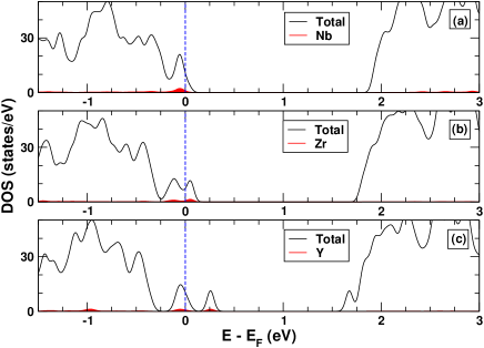
We start by considering Cs adsorption. When Cs is adsorbed on a MoS2 monolayer there is no significant change in the geometry, i.e. the ion binds without distorting the lattice of the host. The DOS presented in Fig. 7(a) shows that the available Cs 6 electron is transferred to the CBM of the MoS2 monolayer, occupying the Mo-4 orbitals. In this case there is no split off at the bottom of the conduction band and the DOS projected over the Cs 6 orbitals appears uniformly spread over a 1.5 eV energy window. This essentially means that Cs adsorbed over a MoS2 monolayer acts as perfect donor. A very similar situation is found for both K and Li, with only minor quantitative differences in the spread of the DOS associated with the shell of the dopant [see Fig.7(b) and Fig.7(c)]. In contrast, the adsorption of H produces a spin-split state 1 eV below the CBM, i.e. roughly at midgap of the LSDA band-gap [see Fig.7]. As such we conclude that H is not a shallow donor for MoS2, in good agreement with the recent theoretical results PRL_2012_109_035503 .
The pairing energies between two Cs atoms and between Nb and Cs are given in Table 2. Our total energy calculations suggest that pairing between Cs atoms is not energetically favorable. On the other hand Cs atoms can reduce their energy if they are adsorbed close to a Nb atom rather than on top of a Mo atom. This can be easily explained with the electrostatic attraction between the two oppositely charged defects. This case of co-doping with Cs and Nb is particularly interesting, since it can be used as a strategy for fabricating p-n junctions, or more generally devices that require both n-type and p-type conductivity. Importantly the DOS of a supercell where a Mo-substitutional Nb impurity is bonded to a Cs adatom appears essentially identical to that of an undoped MoS2 monolayer (see Fig. 8), indicating that charge compensation is very effective. As a consequence our results suggest that an effective strategy for creating p-n hetero-junctions must prevent the formation of Cs-Nb bonding by suppressing the migration of Cs on the surface.
In summary we find that adsorbed alkali metals release their valance electron to the MoS2 conduction band, and that the adsorption energies are large and negative, meaning that the doping will occur easily. Therefore, adsorbed alkali metals, with the exception of H, appear as ideal candidates for doping n-type MoS2. To put this result in context we remark that various experimental studies have demonstrated the possibility of dope n-type bulk MoS2 by intercalating alkali metals Adv_1987_36 . Here we demonstrate that the same is also possible at the single layer level.
Adsorption of molecular ions
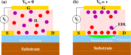
Electric double layer (EDL) transistors with ionic liquids (ILs) employed as gate dielectrics have recently emerged as promising devices, where the electrical properties of a solid can be controlled by electrostatic carrier doping NL_2012_12_2988 ; APL_2011_98_012102 . A schematic diagram for such a device is shown in Fig. 9. By applying a gate bias to the ionic liquid, an electric double layer is formed between the interface of the liquid and the solid (see Fig. 9). Here the polarity of the molecular ions on the surface of the semiconductor can be reversed by changing the polarity of the gate bias. The accumulation of high charge carrier densities is possible (1014 cm-2) and this can be modulated by the applied gate voltage. In some case the accumulation can be so large to lead to phase transitions in the solid. Metal-superconductor and metal-insulator transitions have been demonstrated in KTiO3 NatureNano_2011_6_408 and VO2 NL_2012_12_2988 , respectively. The operation of highly flexible MoS2 thin-film transistors in an ionic liquid gated dielectric has been demonstrated recently NL_2012_12_4013 . Here we discuss the effects of the adsorbed molecular ions on the MoS2 monolayer.
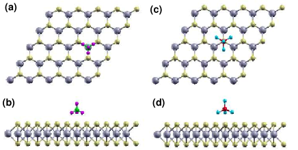
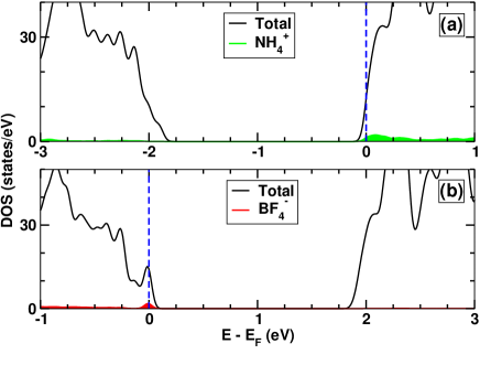
A variety of different ionic liquids are experimentally available. Here we consider NH as cation and BF as anion, and we place them on the MoS2 supercell (see Fig. 10). Such geometry corresponds to an impurity density of 1014 cm-2. We find that the most energetically favorable adsorption site is TS for the cation and TMo for the anion. In Fig. 11(a) the DOS is shown for NH4 adsorption. It can be seen that the NH4 releases one electron into the MoS2 conduction band, resulting in a n-type MoS2 monolayer channel. In contrast, when BF4 is adsorbed, one electron is transferred from MoS2 to the molecule [see Fig. 11(b)]. As a consequence the Fermi energy shifts below the MoS2 VBM, so that the system becomes p-type. This also confirms the fact that the adsorbed molecules are indeed ionized to NH and BF when put on MoS2. In a liquid gated transistor arrangement, the anions/cations are brought close to the surface of the channel by applying a bias at the gate. Therefore, for this system, depending on the polarity of the gate bias the MoS2 is indeed predicted to have a n- or p-type conducting channel. Clearly this effect is maximized for a single layer of MoS2 when compared to thicker structures. In fact, conductivity measurements NL_2012_12_1136 on MoS2 show that EDL gating becomes less efficient when going from a thin layer to bulk. Moreover, depending on the polarity of the bias, it is found that the conductivity indeed switches from n-type to p-type.
III.3 Robustness of the results against the choice of XC functional:HSE06
Finally, in order to verify that the impurity level alignment presented in the previous sections is robust against the level of approximation taken for the DFT exchange-correlation energy, we here repeat our calculations by using the HSE06 functional. The MoS2 lattice constant obtained with HSE06 is 3.155 Å, which is only slightly larger than the LSDA value of 3.137 Å. For a pristine MoS2 monolayer at this relaxed lattice constant HSE06 exhibits a direct band-gap of 2.2 eV (compared to a LDA band-gap of 1.86 eV). This is rather similar to the band-gap obtained by applying the atomic self-interaction correction scheme arXiv:1301.2491 .
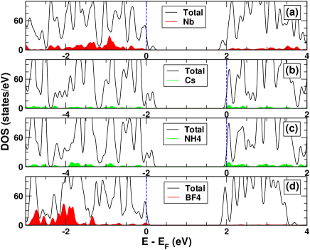
In Fig. 12 we report our results for four representative doping strategies, namely for Nb substitutional doping, as well as for Cs, NH4 and BF4 adsorption. These correspond to the most promising dopants for either n-type or p-type doping as obtained at the LSDA level. The calculations are carried out with the same structures used in the previous sections, in order to make a direct comparison between results obtained with the two functionals used. We note, however, that the MoS2 band-gap is very sensitive to changes in the lattice constant PRB_2012_85_033305 , so that the HSE06 band-gap at the LSDA lattice constant of 3.137 Å becomes 2.31 eV. We find that for all the four cases the main difference between the LSDA and the HSE06 results is just a change in the band-gap, while the impurity levels with respect to the relative Fermi energy are placed at the same position. Therefore we can conclude that the four most promising candidates for doping MoS2 monolayers remain those identified by our initial LSDA analysis.
IV Conclusion
We have carried out a systematic study on the changes to the electronic structure of a MoS2 monolayer induced by various dopants. This study has the aim of identifying possible doping strategies for MoS2 monolayers to be used in devices manufacturing. We have considered first substitutional doping at both the Mo and the S site, as well as doping by adsorption. In general, S substitution with non-metals and Mo substitution with transition metals create deep donor levels inside the band-gap of the MoS2 monolayer for most of the dopants considered. However, with substitutional doping we find that it is possible to obtain p-type MoS2 by replacing a Mo atom with Nb. In contrast n-type doping does not appear possible since we have found deep donor levels for all the substitutions investigated (either at the Mo or the S site). More promising n-type doping can be achieved by adsorbing alkali metals on the surface of MoS2. Finally, as a last class of dopants, we have considered the adsorption of ionic molecules, which occurs during the electric double layer formation in MoS2 embedded in an ionic liquid. These show high potential for inducing large carrier concentrations within the MoS2 monolayer, in the form of both electrons or holes.
Acknowledgments
This work is supported by Science Foundation of Ireland (Grant No. 07/IN.1/I945) and by CRANN. IR acknowledges financial support from the King Abdullah University of Science and Technology (acrab project). We thank Trinity Centre for High Performance Computing (TCHPC) for the computational resources provided.
References
- (1) A.H. Castro Neto and K. Novoselov, Rep. Prog. Phys. 74, 082501 (2011).
- (2) J. A. Wilson and A. D. Yoffe, Adv. Phys. 18, 193 (1969).
- (3) R. H Friend and A. D. Yoffe, Adv. Phys. 36, 1 (1987).
- (4) W. O. Winer, Wear 10, 422 (1967).
- (5) H. Topsøe, B. Hinnemann, J.K. Nørskov, J.V. Lauritsen, F. Besenbacher, P.L. Hansen, G. Hytoft, R.G. Egeberg and K.G. Knudsen, Catalysis Today 107, 12 (2005).
- (6) X. Fang, X. Guo, Y. Mao, C. Hua, L. Shen, Y. Hu, Z. Wang, F. Wu and L. Chen, Chem. Asian J. 7, 1013 (2012).
- (7) K.K. Tiong and T.S. Shou, J. Phys.: Condens. Matter 12, 5043 (2000).
- (8) A. Splendiani, L. Sun, Y. Zhang, T. Li, J. Kim, C.-Y. Chim, G. Galli and F. Wang, Nano Lett. 10, 1271 (2010).
- (9) X. Wang, Y. Ouyang, X. Li, H. Wang, J. Guo and H. Dai, Phys. Rev. Lett. 100, 206803 (2008).
- (10) S.Y. Zhou, G.-H. Gweon, A.V. Fedorov, P.N. First, W.A. de Heer, D.-H. Lee, F. Guinea, A.H. Castro Neto and A. Lanzara, Nature Materials 6, 770 (2007).
- (11) S. Adam, E.H. Hwang, V.M. Galitski and S. D. Sarma, Proc. Nat. Acc. Sci. 104, 18392 (2007).
- (12) A. Ayari, E. Cobas, O. Ogundadegbe and M.S. Fuhrer, J. Appl. Phys. 101, 014507 (2007).
- (13) K.-K. Liu, W. Zhang, Y.-H. Lee, Y.-C. Lin, M.-T. Chang, C.-Y. Su, C.-S. Chang, H. Li, Y. Shi, H. Zhang, C.-S. Lai, and L.-J. Li, Nano Lett. 12, 1538 (2012).
- (14) L. Liu, S. B. Kumar, Y. Ouyang, and J. Guo, IEEE. Trans. Electron. Dev. 58, 3042 (2011).
- (15) B. Radisavljevic, A. Radenovic, J. Brivio, V. Giacometti and A. Kis, Nature Nanotechnology 6, 147 (2011).
- (16) K.F. Mak, C. Lee, J. Hone, J. Shan and T.F. Heinz, Phys. Rev. Lett. 105, 136805 (2010).
- (17) H. Li, G. Lu, Z. Yin, Q. He, H. Li, Q. Zhang, H. Zhan, Small 8, 682 (2012).
- (18) Y.-H. Lee, X.-Q. Zhang, W. Zhang, M.-T. Chang, C.-T. Lin, K.-D. Chang, Y.-C. Yu, J. Tse-Wei Wang, C.-S. Chang, L.-J. Li and T.-W. Lin, Adv. Mater. 24, 2320 (2012).
- (19) Z. Zeng, Z. Yin, X. Huang, H. Li, Q. He, G. Lu, F. Boey and H. Zhang, Angew. Chem. Int. Ed. 50, 11093 (2011).
- (20) Y. Zhan, Z. Liu, S. Najmaei, P. M. Ajayan and J. Lou, Small 8, 966 (2012).
- (21) K. Dolui, I. Rungger and S. Sanvito, Phys. Rev. B 87, 165402 (2013).
- (22) J.D. Fuhr, Andrés Saúl and J.O. Sofo, Phys. Rev . Lett. 92, 026802 (2004).
- (23) J. He, K. Wu, R. Sa, Q. Li, and Y. Wei, App. Phys. Lett. 96, 082504 (2010).
- (24) C. Ataca and S. Ciraci, J. Phys. Chem. C 115, 13303 (2011).
- (25) H. Ji, J. Wei, and D. Natelson, Nano Lett. 12, 2988 (2012).
- (26) Y. Zhang, J. Ye, Y. Matsuhashi, and Y. Iwasa, Nano Lett. 12, 1136 (2012).
- (27) P. Hohenberg and W. Kohn, Phys. Rev. 136, B864 (1964).
- (28) W. Kohn and L. J. Sham, Phys. Rev. 140, A1133 (1965).
- (29) D. M Ceperly and B.J. Alder, Phys. Rev. Lett. 45, 566 (1980).
- (30) J. M. Soler, E. Artacho, J. D. Gale, A. Gracía, J. Junquera, P. Ordejón, and D. Sánchez-Porta, J. Phys.: Condens. Matter 14, 2745 (2002).
- (31) J. Junquera, Óscar Paz, D. Sánchez-Portal and E. Artacho, Phys. Rev. B 64, 235111 (2001).
- (32) N. Troullier and J. L. Martins, Phys. Rev. B 43, 1993 (1991).
- (33) J. Heyd, G.E. Scuseria and M. Ernzerhof, J. Chem. Phys. 118, 8207 (2003); J. Heyd, G.E. Scuseria and M. Ernzerhof, J. Chem. Phys. 124, 219906 (2006).
- (34) P.E. Blø̈chl, Phys. Rev. B 50, 17953 (1994).
- (35) G. Kresse and J. Furthmüller, Phys. Rev. B 54, 11169 (1996).
- (36) H.J. Monkhorst and J.D. Pack, Phys. Rev. B 13, 5188 (1976).
- (37) A. Ramasubramaniam, Phys. Rev. B 86, 115409 (2012).
- (38) T. Cheiwchanchamnangij and W.R.L. Lambrecht, Phys. Rev. B 85, 205302 (2012).
- (39) A. Droghetti, C.D. Pemmaraju and S. Sanvito, Phys. Rev. B 78, 140404(R) (2008).
- (40) J.F. Janak, Phys. Rev. B 16, 255 (1977).
- (41) H.-P. Komsa, J. Kotakoski, S. Kurasch, O. Lehtinen, U. Kaiser, and A. V. Krasheninnikov, Phys. Rev. Lett. 109, 035503 (2012).
- (42) F. L. Deepak, R. P. Biro, Y. Feldman, H. Cohen, A. Enyashin, G. Seifert, and R. Tenne, Chem. Asian J. 3, 1568 (2008).
- (43) K. K. Tiong, P.C. Liao , C.H. Ho and Y.S. Huang, J. Crys. Growth 205, 543 (1999).
- (44) V. V. Ivanovskaya, A. Zobelli, A. Gloter, N. Brun, V. Serin and C. Colliex, Phys. Rev. B 78, 134104 (2008).
- (45) F. L. Deepak et. al, J. Am. Chem. Soc 129, 12549 (2007).
- (46) S. Mathew, K. Gopinadhan, T. K. Chan, X. J. Yu, D. Zhan, L. Cao, A. Rusydi, M. B. H. Breese, S. Dhar, Z. X. Shen, T. Venkatesan and John T. L. Thong, Appl. Phys. Lett. 101, 102103 (2012).
- (47) K.T. Park, J.S. Hess and K. Klier, Journal of Chem. Phys. 111, 1636 (1999).
- (48) K. T. Park and J. Kong, Topics in Catalysis 18, 175 (2002).
- (49) H. T. Yuan, M. Tih, K. Morimoto, W. Tan , F. Wei, H. Shimotani, Ch. Kloc, and Y. Iwasa, Appl. Phys. Lett. 98, 012102 (2011).
- (50) K. Ueno, S. Nakamura, H. Shimotani, H. T. Yuan, N. Kimura, T. Nojima, H. Aoki, Y. Iwasa, and M. Kawasaki, Nature Nanotechnology 6, 408 (2011).
- (51) J. Pu, Y. Yomogida, K.-K. Liu, L.-J. Li, Y. Iwasa, and T. Takenobu, Nano Lett. 12, 4013 (2012).
- (52) W. S. Yun, S. W. Han, S. C. Hong, I. G. Kim, and J. D. Lee, Phys. Rev. B 85, 033305 (2012).