Origin of - and -type conductivity in undoped -PbO: role of defects
Abstract
First principles calculations (GGA) have been applied to study the crystallographic defects in -PbO in order to understand an origin of - and -type conductivity in otherwise undoped -PbO. It was found that deposition in oxygen-deficient environment to be defined in our simulations by the Pb-rich/O-poor limit stimulates a formation of O vacancies and Pb interstitials both characterized by quite low formation energies 1.0 eV. The O vacancy, being occupied by two electrons, shifts the a balance of electrons and holes between these two defects to an excess of electrons (four electrons against two holes) that causes -type doping. For the Pb-poor/O-rich limit, an excess of oxygen triggers the formation of the O interstitials characterized by such a low formation energy that spontaneous appearance of this defect is predicted. It is shown that the concentration of O interstitials is able to reach an extreme magnitude equal to number of the possible defect sites (cm-3). The localized state formed by the O interstitial is occupied by two holes and because there are no other defects in reasonable concentration to balance the hole redundancy, -type doping is induced.
Recent developments in radiation medical imaging technology impose new requirements on photoconductive materials: polycrystalline and amorphous materials are considered for application in flat panel detectors simon with preference given to high Z (atomic number) polycrystalline semiconductors. Among all polycrystalline materials, Lead Oxide (-PbO) is the most promising candidate due to its long history of employment in optical imaging devices book . However, despite such extensive application, properties of -PbO are not well established. There are limited data on the transport properties: the low mobility-time product indicates poor carrier transport rowland and, therefore, it is believed that carrier transport should be controlled by trapping on defects. For application of PbO in real time procedures such as fluoroscopy, transport characteristics are required to be optimized, for which an understanding of the nature of the defects is important. The thermal evaporation technique used for deposition of PbO layers simon ; book presumes a deficiency of atomic oxygen ultimately leading to formation of oxygen vacancies. The conductivity enhancement of PbO samples observed after thermal annealing in an atmosphere of oxygen supports this hypothesis chienes . In our previous studies devoted to defect formation in -PbO single crystal, we confirmed that this compound tends to loose oxygen due to the low formation energy of the oxygen vacancy defects . Oxygen vacancies are found to be occupied by two electrons that leads to a prediction of excess of electrons. The experimentally observed -type conductivity of the PbO layers grown under conditions of oxygen deficiency book ; bigelow ; chienes ; scanlon verifies our theoretical findings defects .
Samples characterized by excess oxygen show the exact opposite behavior: -type conductivity bigelow . The Pb vacancies considered in our previous study defects , although they are occupied by two holes and the oxygen rich conditions promote their formation, can not be responsible for -type doping because of their rather high formation energy. In order to develop the post-growth annealing procedures directed to suppression of the vacancy defects, an understanding of whether the origin of -type conductivity is defect related is urgently required: the application of annealing in oxygen atmosphere becomes questionable, provided it generates new defects, while healing the oxygen vacancies. Therefore, to obtain a real picture a comprehensive study of all type of defects that can be formed under different growth conditions is required. Here we apply first-principles methods for such a study (the Pb-rich/O-poor and Pb-poor/O-rich limits of the growth conditions are considered) with focus on an analysis of the defects being inherent to the -PbO crystal structure, the appearance of the defect states inside the band gap, charged states and formation energies.
I Methods
We study the formation of the defects in -PbO with help of the density functional theory (DFT) provided by the WIEN2k package wien which adopts the full-potential augmented plane-wave + local orbitals method. The generalized gradient approximation (GGA) GGA with the Perdew-Burke-Ernzerhof parametrization was used. The , , and electrons of the Pb atom and and electrons of the O atom have been treated as valence electrons, while lower energy electrons were assigned to the core states (the energy cutoff was -8 Ry). We applied a supercell approach with 108-atom size (333 array of the primitive unit cells). The geometry optimization procedure applied to supercell containing a defect was performed based on minimization of the total energies and forces forces . The residual forces did not exceed 0.5 mRyd/Bohr, the energy convergence limit was set to 0.0001 Ry. The Brillouin zone was covered by a 554 k-point mesh utilizing the Monkhorst-Pack scheme. The product of the atomic sphere radius and plane-wave cutoff in k-space was equal to 7.
The tetragonal lead oxide -PbO is characterized by a layered structure and appears in polycrystalline form upon compound growth simon . The weak orbital overlap of the lone pairs of Pb atoms projected out from each layer holds the PbO layers together new ; new1 , while only valence electrons participate in formation of the hetero-polar bonds with oxygen atoms new1 . GGA tends to overestimate the interlayer separation in the layered structures while underestimating the band gap size. For -PbO system in which the orbital overlap between layers controls the size of the band gap, it results in a compensation effect defects . In particular, for the lattice parameters optimized with GGA (=4.06 Å and =5.51 Å defects ), the band gap is only slightly underestimated, as 1.8 eV to be compared with the experimental value of 1.9 eV exp (for this compound, good agreement of the size of the band gap estimated theoretically with that found experimentally has been pointed out in earlier work as well new ). Application of the experimental value of the lattice parameters causes the band gap to shrink by 0.22 eV defects . Because the size of the band gap is crucial in order to correctly define the appearance of the defect states inside the band gap, the band structure properties have been evaluated for the optimized lattice parameters. However, for calculations of the defect formation energy, an adjustment of the interlayer distance by using the experimental data of the lattice constant ( Åvenk ) has been performed. It was found that only the formation energy of the Pb interstitial is considerably affected by the mismatch in the lattice parameters, caused by the poor incorporation of Pb atom of large atomic radius between the layers (the formation energies of the vacancy defects have been pointed out not to be affected by GGA limitation in our previous work defects ).
II Crystallographic defects in -PbO
Analysis of the literature on defect formation in semiconductors walle and particularly in simple oxides Kotomin , has revealed that additionally to the vacancy defects investigated in our previous study defects , interstitials have to be considered. For crystalline materials, interstitial defects induce a large lattice distortion into their immediate neighbourhood that results in their high formation energy walle . In this regard, the crystal lattice of polycrystalline -PbO is unique, because the distance between weakly interacting layers is large enough to accommodate a foreign atom ( Åvenk ). Therefore, along with the vacancy defects, formation of the interstitials is expected to be inherent to the -PbO lattice.
We start from a short description of the vacancy defects already investigated in our previous work defects . The O vacancy () is occupied by two electrons localized on the four nearest Pb atoms with maximum of the electron density to manifest at the vacancy site (see the electron density distribution in Fig. 1 (a)). The O vacancy can appear in three charged states (0, 1+, 2+). The localized state generated by the O vacancy is located deep inside the band gap at ()-=1.03 eV, where is the top of the valence band. In contrast, the Pb vacancy creates a localized state occupied by two holes and the defect level appears close to the valence band top at ()-=0.1 eV. The electron density is spread between O and Pb atoms showing long defect tails (see Fig. 1 (b)) which is not surprising taking into account the defect level appearance close to the valence band top (see Fig. 2). The Pb vacancy has also three charge states (0, 1, 2) but its charge states would be of negative sign, i.e. ionization of the vacancy occurs through an electron gain. The effect of mismatch of the lattice parameters on location of the vacancy-induced states was examined. It is found that a position of the defect states relatively to the valence band top is not affected with application of the experimental lattice parameters: since the vacancy states are localized entirely within single layer, an alteration in the interlayer interactions has almost no impact on its property defects .
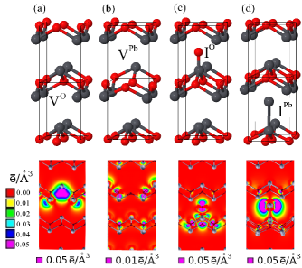
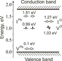
There are two interstitial defects to be considered in -PbO crystal lattice, the O and Pb interstitials. Binding of the O interstitial () to the host occurs with participation of the lone pair Pb: electrons from the host (the lone pair Pb: in -PbO is chemically active new1 ): the bond is made between lone pair Pb: electrons of the host and O: empty orbital of oxygen atom. The O: empty orbital appears upon excitation of the ground state O: to the O∗: state. The lowest energy state is achieved when the O interstitial is positioned just above the Pb atom (see Fig. 1(c), the bond length is 2.03 Å). Inside the band gap, the localized state is located above the midgap at ()-=1.27 eV (see Fig. 2). This localized state can accommodate up to two extra electrons and, therefore, there are three charge states (0, 1, 2) are assigned to it.
The energetically favourable position of the Pb interstitial () in the lattice is similar to the O interstitial, i.e. on top of the Pb atom. The Pb interstitial is exited from the ground state of configuration Pb: to the Pb∗: state thus allowing and electrons to contribute in bond formation with the host. The host Pb atom participates in bonding, again with its Pb: electrons (the bond length is 2.9 Å). The originated defect state is occupied by two electrons which are Pb: electrons belonging to (see Fig. 1 (d)). Since each electron stays on its own orbital, Hund’s rules dictate the ferromagnetic ordering of these electrons my_magn . The spin-polarization energy defined as the energy difference between the spin-unpolarized and spin-polarized states is found to be =0.235 eV that indicates the stable triplet ground state my_magn . The Pb interstitial induces a localized state inside the band gap and spin-polarized solution separates the occupied and unoccupied states as ()-=0.99 eV and ()-=1.51 eV (see Fig. 2), respectively. Ionization of the defect state formed by the Pb interstitial can occur as through electron gaining ((1) for one electron added and (2) for two electrons), so, through an excitation of existing electrons. Overall, there are five charged states (2+, 1+, 0, 1, 2) can be considered for the Pb interstitial.
Since properties of the interstitial defects are expected to depend on the interlayer distance, an alteration in position of the defect states inside the band gap with implementation of the experimental lattice parameters has been investigated. It was found that for the O interstitial the defect state is shifted only by 0.05 eV outwards . However, the effect is more pronounced for the Pb interstitial because of larger atomic radius of Pb atom. Thus, the state occupied by electrons appears at ()-=0.97 eV while empty state at ()-=1.25 eV. Moreover, for the defect state like Pb interstitial, DFT is known to delocalize the defect wave function and underestimate the splitting between the unoccupied and occupied states that occurs due to self-interaction of the unpaired electrons book1 . Therefore, defect wave-function localization has been additionally examined with Hartree-Fock (HF) approach applied directly to the unpaired electrons HF ; book1 (in this way the accuracy provided by DFT is preserved). Indeed, it resulted in stronger localization and, therefore, enhanced splitting of the defect states such as ()-=0.54 eV for the occupied state and ()-=1.66 eV for the empty state. However, since the experimental lattice parameters and HF correction have opposite effect on the defect wave function localization, application of both leads to compensation effect in level splitting such as appearance of the defect states in the band gap is ()-=0.54 eV for the occupied state and ()-=1.22 eV for the empty state. Since the band gap size is reduced by 0.22 eV defects , location of these defect states in respect to bottom of the conduction band is very close to that found with GGA (see Fig. 2).
We have established that some defects can act as a donor impurity (), others as acceptors ( and ), while can be both an electron donor () and an acceptor (). An ability of defects to appear in several charge states encourages the electron exchange between defects: the electron donor compensates missing electrons on the acceptor. The process of the charge exchange defines the energetically favorable charge state for defects appearing upon compound growth.
III Formation energy of defects
The main way to identify formation of defects inherent to the crystal structure is to compare the formation energies of different defects, as particularly this parameter is a measure of the defect concentration. The formation energy of a defect in charge state (+2/+1/0/-1/-2) can be defined as walle
| (1) |
where and are the total energy of the system containing the single defect and defect-free system, respectively. indicates a number of -atoms removed () or added (), while is the chemical potentials. () is the position of the Fermi level relative to the valence band maximum () which has to be corrected by (for details see Ref. walle ).
For calculation of the formation energy of the native point defects , the supercell approach has been applied. In order to minimize an interaction between a defect and its periodic replicas, the sufficiently large supercell (333) is used for simulation of defects. The geometry optimization procedure has been applied as for the neutral supercell (the total energy of the system corresponds to ) and so after defect has been charged: energy has been evaluated for the defects in the different charge states (+2/+1/0/-1/-2) (for details see walle ). An alignment of the top of the valence band () for supercell with charged defect to that in the bulk is performed with help of the correction term walle . Since for accurate calculation of the formation energy of interstitial defects the mismatch in the interlayer distance (=5.51 Å) occurring for the lattice parameters optimized with GGA in comparison to the experimental data (=5.07 Åvenk ) is essential, the experimental value has been used for those calculations. In this case, an application of the so-called band gap error togo is required to compensate for a reduction of the band gap size defects . For vacancies, because of their weak interactions with the opposite layer, the formation energy would be rather insignificantly affected by the interlayer distance mismatch, and the same argument works for the vacancies appearing on the surface of the single crystal (platelet). However, for interstitial defects because of their strong interaction with the opposite layer, the formation energy would be altered upon appearance on the platelet’s surface. For defects on surface, slab’s thickness was four layers, its width was 10 Å, while distance between slabs was 14 Å.
To simulate the deficit and excess of oxygen, the Pb-rich/O-poor and Pb-poor/O-rich limits have been applied in evaluation of the chemical potentials. The chemical potentials have been found for the Pb-rich/O-poor limit as =(O atom)+, where is the standard enthalpy of formation of PbO compound, while is determined from =+. For the Pb-poor/O-rich limit the chemical potentials are =(Pb atom)+ and, similarly, is found from =+. The standard enthalpy of formation =-2.92 eV per Pb-O pair has been calculated elsewhere defects applying a formalism described in details earlier walle .
We have calculated the formation energies of the different defects in the relevant charge states and our results as a function of the Fermi level position for the Pb-rich/O-poor and Pb-poor/O-rich limits are shown in Fig. 3. Since the Fermi level defines a probability for electron to occupy the defect state, the formation energy of the charged state is a function of Fermi level position inside the band gap. As deviates in a range defined by (in real growth conditions to be controlled by the partial pressure of reactants) it induces a shift of the formation energies. The concentration of the defects can be estimated through their formation energies as exp, where is the Boltzmann constant, K is the deposition temperature and is the concentration of sites available for defects to be formed.
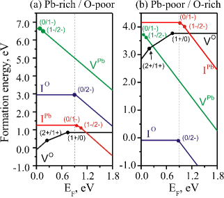
For the Pb-rich/O-poor limit (see Fig. 3 (a)), the formation energies of the O vacancy () and the Pb interstitial () appear to be much lower than that for other defects and, therefore, these defects are expected to dominate. The defect concentrations estimated for their zero charge states are cm-3 for the O vacancy and cm-3 for the Pb interstitial. For the Fermi level assigned to the midgap, the (0, 1+) and (0, 1-) states are energetically preferable for the O vacancy and the Pb interstitial, respectively. Since the thermodynamic transition is found to occur almost at the midgap, it indicates a potential for both states to be formed during the compound growth. However, to be ionized, has to dispose of its electron and therefore, the appearance of the charge state would naturally depend on the presence of the electron acceptor. For the Pb interstitial, we have calculated the formation energy for the five states (2+, 1+, 0, 1, 2). Since the formation energy of the (1-) state that occurs when an extra electron is added, is significantly lower than that when an electron is removed (=3.98 eV for at midgap), the and states have been disregarded. The thermodynamic transition occurs close to the midgap and, therefore the charge states (0, 1) appear to be the preferable states. To become ionized to the (1) state, has to gain an electron (electron acceptor).
Therefore, the charge exchange between and is possible as one of them can work as an electron donor while other as an acceptor. The concentration of ionized states to manifest upon charge exchange would be limited by the defect of lower concentration, i.e. by the Pb interstitial (cm-3). It is important to emphasize that the balance of electrons and holes occupying both defect sites in either combination of the charge states (/ or /) is always shifted to a higher population of electrons (four electrons against two holes). Therefore, with respect to the conductivity type, redundant electrons induced by the O vacancies would cause -type doping of -PbO at the Pb-rich/O-poor limit to be in agreement with our previous studies defects . In the non-equilibrium electron gas (photogenerated or injected carriers), the ionized O vacancies and the Pb interstitials in both charge states , would work as trapping centers for electrons in the conduction band.
For the Pb-poor/O-rich limit, only the O interstitial, , possesses a low formation energy, while the formation energies of other defects (, and ) are higher than 3.0 eV. In fact, the formation energy of being so closed to zero implies the spontaneous appearance of this defect such as the defect concentration can become equal to the concentration of the possible defect sites (cm-3 Nsites ). The O interstitial in its neutral charge state misses two electrons and, to be ionized to the charge states (1-/2-), has to acquire electrons. Since the thermodynamic transition occurs close to the midgap, potentially can be formed in the charge states (1-,2-). However, because the concentration of centers of the donor type (, ) is negligible, the O interstitial is expected to occur primary in its state. The state would act as a trap for the non-equilibrium electrons in the conduction band. Therefore, under growth conditions corresponding to the oxygen excess, the high concentration of defects each to be occupied by two holes, would be able to cause -type doping. Moreover, the state formed by the O interstitial is characterized by a quite delocalized nature (see Fig. 1 (c)): the long defect tails in combination with the high defect concentration would results in strong defect-defect interaction potentially leading to formation of the defect band.
It is also important to emphasize that all investigated defects, , , and being considered in bulk -PbO would be inherent to surface of the single crystal (platelet). For some defects, the formation energy is found to be lowered when they are placed on the platelet surface. The strongest effect is observed for the Pb interstitial for which the formation energy drops by 1.0 eV. For the vacancies, the formation energy is only affected provided they appear at the edge of the platelet (for example, it is reduced by 0.3 eV for oxygen vacancy). The reduction of the formation energy at the platelet edge is a result of surface reconstruction leading to formation of the Pb-O double bonds instead of single bonds. Since the balance of electrons and holes occupying the defect sites is not affected by the formation of surface states, the considered phenomenon of the - and -doping remains valid. There is one more interesting feature to be examined, which is defect pairing. For the Pb-rich/O-poor conditions, the pairing may occur between and defects, and is promoted by a lowering of the formation energy by 0.84 eV. Such a pair - still forms two defect levels at ()-=1.22 eV and ()-=0.66 eV and each level is occupied by two electrons. For the Pb-poor/O-rich conditions, the interaction between and potentially can occur but because each localized state is occupied by two holes, such interaction is repulsive. Under equilibrium growth conditions, the formation energy of and would become comparable, indicating a possibility of their pairing as well divacancy . This combination of defects is unique as it induces vanishing of the dangling bonds and, therefore, occurs without generation of a defect state inside the band gap. Moreover, because the formation energy is lowered by 1.47 eV upon defect pairing, it indicates the pairing to occur not only during the compound growth but also as a post-growth migration of the O vacancy towards the Pb vacancy.
IV Conclusion
Our study on the formation of defects in single crystal -PbO has revealed that some defects under certain growth conditions would appear in significant concentration causing - or -type doping of compound. In particular, for the Pb-rich/O-poor limit a formation of the and defects are found to dominate with concentrations of cm-3 and cm-3, respectively. The obtained defect concentrations are in good agreement with concentration of the localized states estimated experimentally (-cm-3 book ). It was established that accumulation of electrons on sites of the and defects results in -type doping of -PbO. For the oxygen excess created during the compound growth (Pb-poor/O-rich limit), another defect is found to manifest which is the O interstitial. The concentration of is predicted to approach the highest limit because its formation energy is around zero, i.e. the defect concentration may become equal to the number of the possible defect sites. Since each is occupied by two holes, its high concentration would result in -type doping of -PbO. Moreover, such low formation energy of the O interstitial might be a problem for the post-growth procedures such as annealing. We predict that annealing in an atmosphere of oxygen addressed to heal O vacancies would generate new defects such as O interstitials. With respect to the transport properties, the negative impact of the dominant defects, , and would become apparent because these defects induce the states close to the midgap: severe trapping of non-equilibrium electrons from the conduction band is expected.
V Acknowledgement
Financial support of Ontario Ministry of Research and Innovation through a Research Excellence Program “Ontario network for advanced medical imaging detectors” is highly acknowledged.
References
- (1) Simon M, Ford R A, Franklin A R, Grabowski S P, Menser B, Much G, Nascetti A, Overdick M, Powell M J and Wiechert D U 2005 IEEE Transactions on Nuclear Science 52, 2035.
- (2) Photoelectronic imagining devices, V. 2 (1971), Eds. L.M. Biberman, S. Nudelman. (Plenum Press, New York-London); Broek J 1967 Philips. Res. Rep. 22, 367.
- (3) Rau A W, Bakueva L and Rowlands J A 2005 Med. Phys. 32 3160.
- (4) Hwang O, Kim S, Suh J, Cho S and Kim K 2011 Nuclear Instruments and Methods in Physics Research A 633 S69.
- (5) Berashevich J, Semeniuk O, Rubel O, Rowlands J A, Reznik A 2013 J. Phys.: Condens. Matter. 25, 075803.
- (6) Bigelow J E and Haq K E 1962 J. Appl. Phys. 33 2980.
- (7) Scanlon D O, Kehoe A B, Watson G W, Jones M O, David W I F, Payne D J, Egdell R G, Edwards P P and Walsh A 2011 Phys. Rev. Lett. 107 246402.
- (8) Blaha P, Schwarz K, Madsen G K H, Kvasnicka D and Luitz J Wien2k: An Augmented Plane Wave + Local Orbitals Program for Calculating Crystal Properties: Karlheinz Schwarz, (Techn. Universität Wien, Austria, 2001)
- (9) Perdew J P, Burke K and Ernzernof M 1996 Phys. Rev. Lett. 77 3865.
- (10) Yu R, Singh D and Krakauer H 1991 Phys. Rev. B 43 6411.
- (11) Payne D J, Egdell R G, Law D S L, Glans P-A, Learmonth T, Smith K E, Guo J, Walsh A and Watson G W 2007 J. Mater. Chem. 17 267.
- (12) Walsh A, Payne D J, Egdell R G and Watson G W 2011 Chem Soc Rev 40 4455.
- (13) Thangaraju B and Kaliannann P 2000 Semicond. Sci. Technol. 15 542.
- (14) Venkataraj S, Geurts J, Weis H, Kappertz O, Njoroge W K, Jayavel R and Wuttig M 2001 J. Vac. Sci. Technol. A 19 2870.
- (15) Van der Walle C G and Neugebauer J 2004 J. Appl. Phys. 95 3851.
- (16) Kotomin E A, Popov A I 1998 Nucl. Instr. and Meth. in Phys. Res. B 141, 1.
- (17) Kokalj A 2003 Comp. Mater. Sci. 28 155.
- (18) Berashevich J and Reznik A, arxiv:1304.2945.
- (19) Advanced Calculations for Defects in Materials: Electronic Structure Methods (2011), Eds. Alkauskas A, Dek P, Neugebauer Jrg, Pasquarello A, Van de Walle, Chris G. (Weinheim, Germany: Wiley-VCH Verlag & Co), Ch. 11.
- (20) d’Avezac M, Calandra M, Mauri F 2005 Phys. Rev. B 71, 205210.
- (21) Togo A, Oba F, Tanaka I and Tatsumi K 2006 Phys. Rev. B. 74 195128.
- (22) Berashevich J, Semeniuk O, Rowlands J A and Reznik A 2012 EPL 99 47005.
- (23) Berashevich J, Rowlands J A and Reznik A 2013 EPL 102 47002.
- (24) The standard procedure has been applied to determine : , where is the Avogadro’s number, is the molar mass and is the density found for -PbO at http://en.wikipedia.org/wiki/Lead(II)oxide.