Two-dimensional simulations of temperature and current-density distribution in electromigrated structures
Abstract
We report on the application of a feedback-controlled electromigration technique for the formation of nanometer-sized gaps in mesoscopic gold wires and rings. The effect of current density and temperature, linked via Joule heating, on the resulting gap size is investigated. Experimentally, a good thermal coupling to the substrate turned out to be crucial to reach electrode spacings below 10 nm and to avoid overall melting of the nanostructures. This finding is supported by numerical calculations of the current-density and temperature profiles for structure layouts subjected to electromigration. The numerical method can be used for optimizing the layout so as to predetermine the location where electromigation leads to the formation of a gap.
pacs:
66.30.Qa, 73.63.RT, 44.10.+i, 02.70.BfI Introduction
Electromigration leads to the formation of voids and hillocks in metallic conductors by thermally assisted ion diffusion under the influence of an applied electric fieldHo and Kwok (1989). For more than a decadePark et al. (1999), this process has been employed to deliberately form gaps of the order of a few nanometers only in microstructures. These gaps can be used to incorporate molecules in a source-drain channel. The planar geometry facilitates the integration of gating electrodes that are essential for a systematic characterization of electronic transport through molecules.
Initially, electromigration was performed at cryogenic temperatures and reported to yield irregularly shaped slits with a narrowest separation . From low-temperature current-voltage measurements, nm was estimatedPark et al. (1999, 2000). However, metallic clusters often remained in the generated gapHouck et al. (2005); Heersche et al. (2006); van der Zant et al. (2006). By working at room temperature, the cleanliness of the gaps could be improved, while the simultaneous implementation of a feedback-control still allowed the generation of nanometer-spaced electrodesStrachan et al. (2005); Esen and Fuhrer (2005); Strachan et al. (2007). We used a realization of this latter technique aimed at the control of the power dissipated while a gap is being formed. The procedure is similar to the one described in Ref. Hoffmann et al., 2008. Our aim is to extend the technique used so far for gaps in single wires to more complicated structures, e. g., to form gaps in the two arms of a ring connected by leads at opposite sides.
To obtain a high yield of nanogaps, the experimental parameters have to be optimized with respect to two competing objectives. On the one hand, the temperature and the current density have to be raised sufficiently for material transport to occur on a reasonable time scale. On the other hand, Joule heating has to be limited to avoid melting of the metal structure, which would lead to droplet formation due to surface tension and to an unwanted increase in electrode spacing.
In our experiments, we find a clear dependence of the resulting gap size on the thermal coupling of the electromigrated structure to the cold substrate. We present a numerical model which leads to a plausible explanation of this finding. It maps the current density and the excess temperature in the voltage-biased structure taking into account the heat flow to the substrate. The calculations can be used to optimize the sample geometry so as to predetermine the location where electromigration leads to the formation of voids and the structure is finally going to break.
II Experimental Observations
All samples used for this work were prepared by standard e-beam lithography on commercially available, slightly p-doped (boron, resistivity: Ωcm) silicon substrates. Their surface was either covered by 400 nm thermally grown SiO2 or merely by native silicon oxide. Here, we focus on samples made from 30 nm thick gold deposited by electron-beam evaporation without any additional adhesion layer.
Electromigration was performed at room temperature and mostly at ambient pressure. Some experiments were carried out in the high vacuum (Pa) of a scanning electron microscope (SEM) for in-situ monitoring of the electromigration process. The resulting gap size, however, did not depend on the background pressure. The active feedback-control loop was realized by ramping a voltage across the sample and measuring its resistance in a four-point configuration. Upon detection of a certain change of %, the voltage was set back to a safe value immediately by the control software and the voltage ramp was reinitialized. At an advanced stage of the process a sudden change of resistance by several orders of magnitude indicates rupture of the metallic current path and the procedure is stopped.
(a) (b)
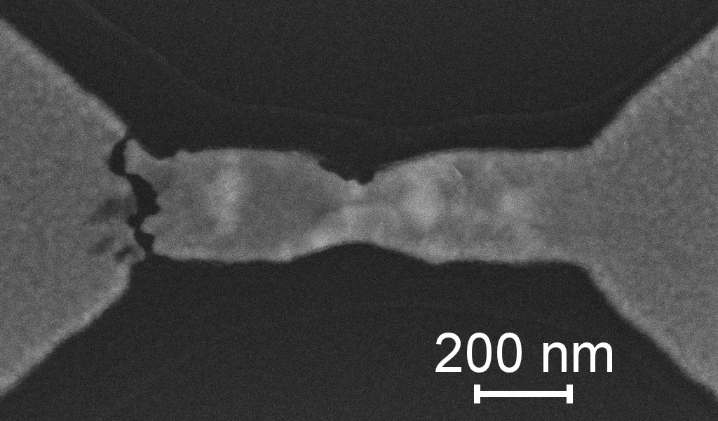
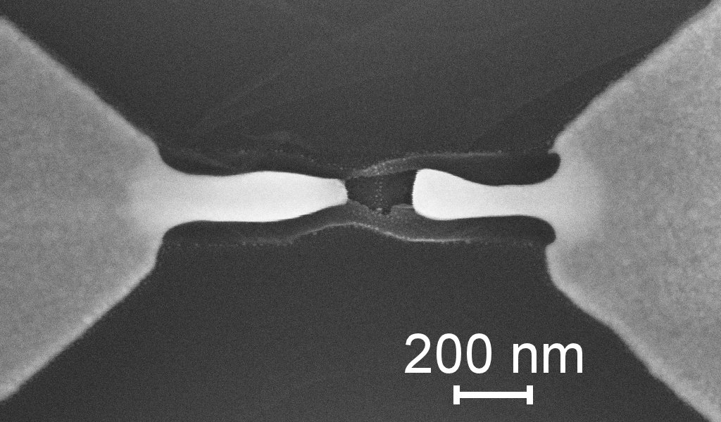
In this paper we want to address the issue of Joule heating during electromigration. Its effect manifested itself mainly in two aspects of our experiment. On the one hand, SEM imaging after gap formation revealed that metallic structures on silicon wafers covered by a 400 nm thick thermally grown silicon oxide layer tend to show signs of melting. Consequently, the resulting electrode separation is considerably above 10 nm. A typical example is shown in Fig. 1 (b). Samples electromigrated on silicon covered by native oxide, however, display the intended formation of voids and hillocks leading to the opening of an irregular gap, whose expansion lies below the resolution of the SEM, i. e., nm. An example is shown in Fig. 1 (a). On the other hand, as can be seen in the same figure, the samples were usually disrupted near their cathode end and not at the constriction prestructured for this purpose at the center of the wire.
Breaking at the cathode side is a common observation in straight wiresBlech and Meieran (1967, 1969); Ho and Kwok (1989); Heersche et al. (2007). It arises because electromigration is due to two mechanisms leading to atom transport in opposite directions. First, atom transport it is directly driven by the electrostatic force acting on the positively charged atom cores in the applied electric field. This mass transport is directed towards the cathode. Second, the cores are driven by the so called “electron wind”, i. e., the momentum transfer from the conduction electrons to defects in inelastic scattering events. The net contribution of these impacts is parallel to the electron current. In gold the motion due to the electron wind predominates and thus material is effectively transported towards the anode. Since the amount of material flow depends strongly on temperature, electromigration is enhanced by Joule heating in those parts of the sample where the current density is highest and leads to depletion of material at the cathode side of narrow constrictions in the current path.
The purpose of the constriction shown in the center of Fig. 1 (b) is to enhance the current density and create a hot spot at a predefined position. Electromigation was expected to lead to a break junction at this very location which, however, was not observed. Apparently, the conditions at the lead-nanowire-junction have to be taken into account more carefully. In the next section we present a model to calculate the temperature profile for a given sample layout which takes into account the heat flow from the metal film to the leads as well as to the substrate. The latter part is of utmost importance as indicated by our experimental observations presented in Fig. 1.
III Calculation of the heat distribution
The temperature in a voltage-biased sample is enhanced due to Joule heating. We present a model to quantify this effect. It is applicable to metallic structures of constant thickness , sheet resistance , and thermal conductivity . Heat is carried along the metal film to the leads and through an insulating barrier of thickness and thermal conductivity , where the condition naturally holds. The structure is supported below the barrier by a thick substrate with thermal conductivity . The substrate is assumed to be thermally well coupled at the back side to a heat reservoir at ambient temperature. It is heated from the top by the power flowing through the barrier which results from the dissipation in the metallic structure. The situation in the substrate is therefore intrinsically three dimensional. However, we can safely assume that the temperature in the metallic structure itself does not vary significantly perpendicular to the film plain (owing to ). The temperature rise in the substrate depends strongly on the barrier thickness and is significant for small only. We postpone the discussion of thicker barriers to the end of this section and assume first that the temperature varies linearly across the insulating barrier, i. e., we consider a laminar heat flow across the insulator perpendicular to its interfaces with the metal film and the substrate. The numerics for the metallic film is reduced to a two-dimensional problem obeying the modified Poisson equation:
| (1) |
Here is the temperature elevation relative to the base temperature of the unbiased sample, the power density, the two-dimensional current density, and the temperature at the interface between of the substrate and the barrier. The left-hand side of Eq. (1) describes the heat balance in the metallic film, while the right-hand side is equal to the loss due to heat flow to the substrate. The latter depends implicitly on which itself obeys the three-dimensional Laplace equation (describing the source-free heat flow in the thick substrate)
| (2) |
subjected to mixed boundary conditions. At the interface with the insulating barrier we have
| (3) |
where is the gradient perpendicular to the interface. At all other boundaries we approximate by zero. Equations (1) and (2) form a set of mutually dependent relations.
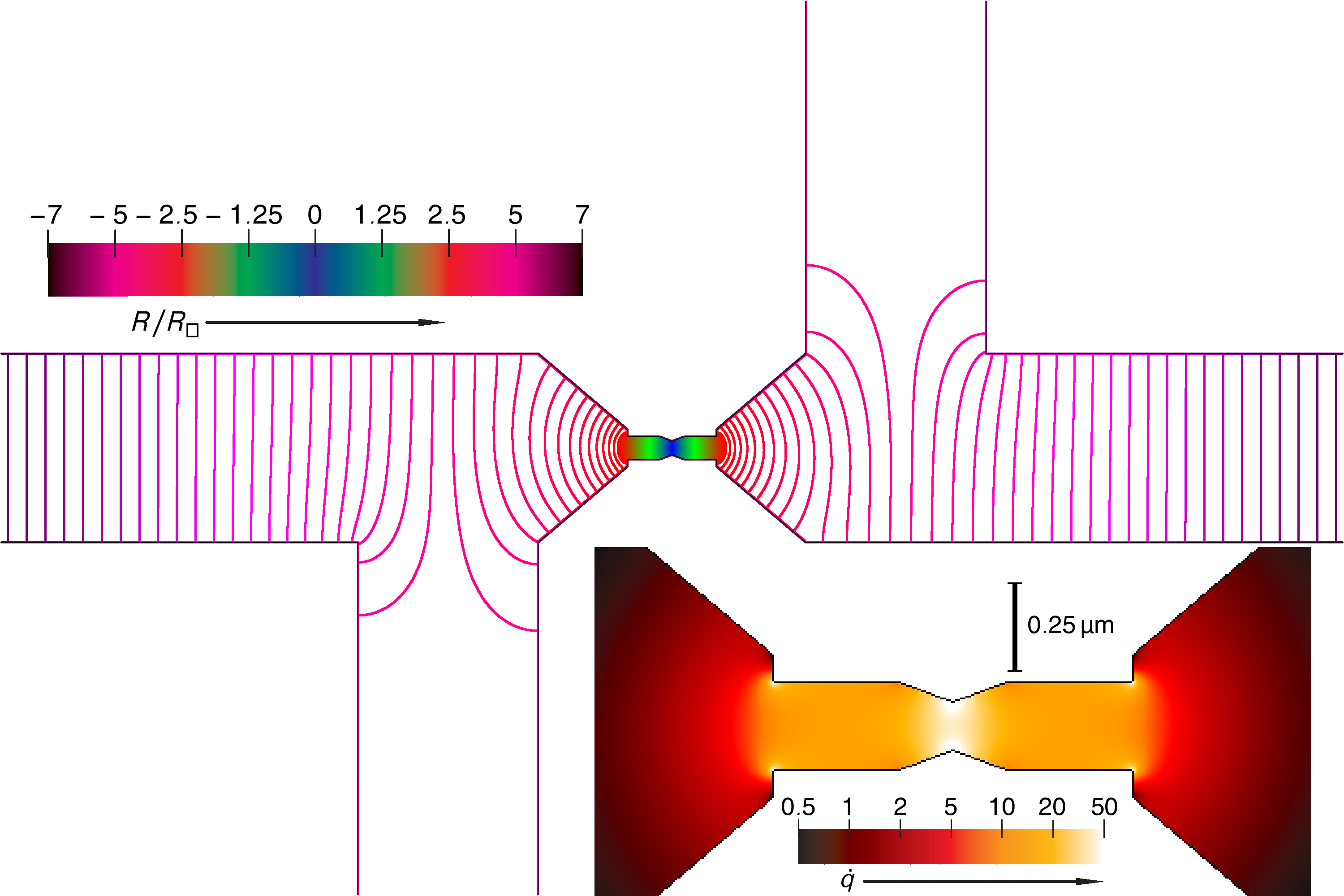
We find it convenient to solve this set of equations by a finite-difference method on a square lattice and discretize the relevant parts of the metallic structure with a predefined cell size sufficiently small to capture all fine details. For this purpose we use an appropriate rectangular cutout of the e-beam lithography design file, which covers the area of highest current densities. For the examples presented below, a cell size between 1 nm and 5 nm turned out to be reasonable, with several million cells within the cutout. The current and voltage leads (cf. horizontal and vertical structures, respectively, emanating from the center in Fig. 2) have constant cross section and extend beyond the cutout. In addition the length of the leads included in the explicit calculation exceeds their width. These measures guarentee that the equipotential lines beyond the cutout generated by an electromotive force between source and drain current leads run perpendicular to the latter.
Before solving Eqs. (1) and (2) we have to calculate the current density which enters the second term on the left-hand side of Eq. (1). is directly related by to the potential , which in turn obeys the Laplace equation with mixed boundary conditions. We solve the latter equation by successive overrelaxation (SOR)Press et al. (2007). For edges of the metallic structure internal to the explicitly treated area as well as for sections of voltage probes with its border we have von-Neumann conditions, . At the section of the source and drain leads with the border we apply the actual bias and , respectively. After solving the Laplace equation subjected to these boundary conditions, the total current can be calculated, where the integral runs along an arbitrary line cutting the source-drain path. It is convenient to normalize by , since directly reflects the “number of squares” between different points within the metallic structure, i. e., the length-to-width ratio of a strip which would acquire an equivalent voltage drop if biased by the same current. Figure 2 shows the result of the calculation for a layout typically used in our experiments. The inset of this figure displays the power density in the center of the structure. The notch in the middle does indeed lead to the intended peak of the power density at this position (and of the current density that drives electromigration). However, a similar peak is found at the crossover from the funnel-shaped leads to the narrow wire as indicated by the four lightly colored spots at the rectangular corners in the inset of Fig. 2. This is due to the well-known divergence of the electric field strength at cornersJackson (1999). In our numerics, this divergence is limited only by the finite cell size used in the finite-difference method as corners are infinitely sharp in the layout. In practice, e-beam lithography leads to a minimal radius at corners set by the finite resolution of the process and the granularity of the crystalline metallic layers. This radius sets the scale of the actual current-density enhancements. It can thus be expected that the current density reaches the same order of magnitude at each concave corner. The precise value depends, however, on the opening angles and can be tuned by proper design. Consequently, rectangular corners as the ones visible in Fig. 2 should be avoided in the strongly heated parts of the structure, unless a starting point for electromigration is intended. We are going to comment further on this issue in the next section.
Having at hand, we solve Eqs. (1) and (2) simultaneously by an iterative procedure. Starting with we first relax Eq. (1) at constant to get an updated estimate for . The boundary conditions for the structure edges are again of von-Neumann type, . Special care has to be taken to treat the heat flow at the border of the cutout. Owing to the aforementioned homogeneous nature of the leads extending beyond this border, the heat-flow problem is essentially one dimensional hereDurkan (2007). In long leads the temperature along the wire direction approaches exponentially a steady-state value of
where is the current in the specific lead of width . In general, the substrate temperature in this equation has to be determined self-consistently as it results from the heat flow caused by the last term. However, is naturally small compared to more strongly heated zones below spots of high current density. We ignore small variations of at the border of the cutout and take in the above formula for a self-consistently calculated value. The functional dependence of the temperature along the leads is then given by
| (4) |
Here is a spatial coordinate along the current direction entering the cutout at , is the temperature of the cross section at , and is the length scale of relaxation towards the asymptotic . From Eq. (4) the boundary condition of Eq. (1) at the cutout frame can be deduced,
| (5) |
Eq. (5) completes the boundary-value problem defined in Eq. (1) and is used in a successive overrelaxation loop to update . In the next step of the iterative procedure we fix in Eq. (3) and update via Eq. (2). Here, successive overrelaxtion would fail since the 3d nature of heat relaxation in the substrate leads to an intractably large number of cells in the discretization step. The final goal of our calculation, however, is the determination of defined in the 2d plane of the metallic structure. To this end we need to know at the interface between the substrate and the barrier only. Let be the solution of in the 3d half-space of obeying Dirichlet conditions and von-Neumann conditions at , . Due to the linearity of the Laplace equation we can write down immediately the solution of Eq. (2) obeying the boundary condition of Eq. (3),
| (6) |
The integral is restricted to the plane . Thus, the calculation of at the interface requires the knowledge of at the interface only as well. In this way Eq. (6) is reduced to a two-dimensional convolution which can be solved numerically by discrete Fourier transforms (DFT) for which fast algorithms exist. Our problem is thus reduced to the determination of . Details of this calculation are given in the appendix.
Eq. (6) can now be used to update . Note, however, that Eq. (6) does define only implicitly. Therefore a further relaxation loop is required. In each iteration of this loop the convolution on the right-hand side is calculated employing the convolution theorem by two consecutive DFT steps. The result is subsequently used to update . In the course of the iteration, the changes in get smaller and the loop is terminated after sufficient accuracy has been obtained. This ends the first round of our overall iterative procedure. In the following iterations we proceed by using Eq. (1) at constant to update and Eq. (2) at constant to update . The procedure converges to a self-consistent solution after several iterations.
So far we have developed a model applicable for thin barrier thickness . From now on, we refer to this particular approximation as Approx. I. In the next section we present results showing that indeed substrate temperature and follow each other closely for small and the a-priori approximation of a laminar heat flow perpendicular to the interface between substrate and barrier is justified in this case. However, is a monotonically decreasing function of while at the same time rises monotonically Moreover, at small it is possible to heat the substrate rather locally by the large power density resulting from a notch as, e. g., the one in the center of the test structure displayed in Fig. 2. If is increased the power is delivered to the substrate more evenly and the temperature distribution tends to smooth out (with a small enhancement only even at the center). The temperature difference soon becomes so large that on the right-hand side of Eq. (1) can safely be neglected. In this case, the vertical nature of the heat flow is lost and the problem of the heat distribution in the isolating barrier has to be treated more precisely. Fortunately, this can be done by the same method introduced so far. For thicker barriers we take the temperature at the interface of the substrate with the barrier as unelevated, the barrier now stays cold at its back side and takes thus the role formerly played by the substrate. The set of Eqs. (1), (2), and (3) now reads
| (7) |
where is the temperature drop across a slice of the barrier of infinitesimal thickness . In the finite-difference treatment of the problem we set equal to the discretization cell size. In Eq. (III) represents the 3d temperature profile in the barrier. As such, it is defined at the interface of the barrier with the metal film, too. At this interface, equals (in the numerics it differs marginally since the infinitesimal is approximated by a variable of finite extent). The thickness enters this approximation via a modification of in Eq. (6), which we label . It still obeys the Laplace equation , now in the barrier, i. e., for , but the Dirichlet condition is replaced at by . In this way we approximate the temperature at the interface between barrier and substrate by the base temperature of the unbiased sample. We refer to this type of approximation as Approx. II in the following section. The calculation of on a rectangular grid used in the finite-difference approximation is explained in the appendix.
IV Results
The model developed in the last section can be used to optimize structure layouts intended for the formation of narrow break junctions at well defined locations by deliberate electromigation. In this section we present some examples.
First we want to address the question why metallic structures on a thicker silicon oxide layer are more likely to melt during the electromigration process than samples on native SiO2. For that purpose we calculate the excess-temperature map for the sample geometry shown in Fig. 2 for varying barrier height . For definiteness we consider gold structures (W/KmPowell et al. (1966)) with a layer thickness of nm, approximate the thermal conductivity of the substrate by the typical value of silicon at room temperature, W/KmGlassbrenner and Slack (1964), and vary between 1 nm and 2.5 µm. For the thermal conductivity of the barrier we use that of thin SiO2 films at room temperature, W/KmKleiner et al. (1996).
(a) (b)
(c) (d)
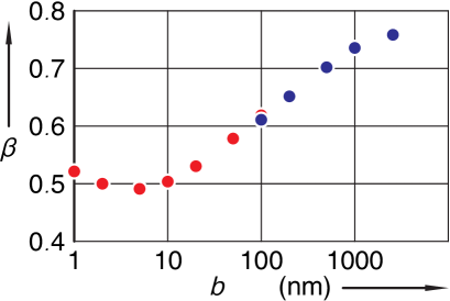
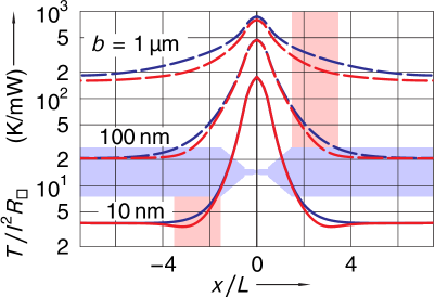
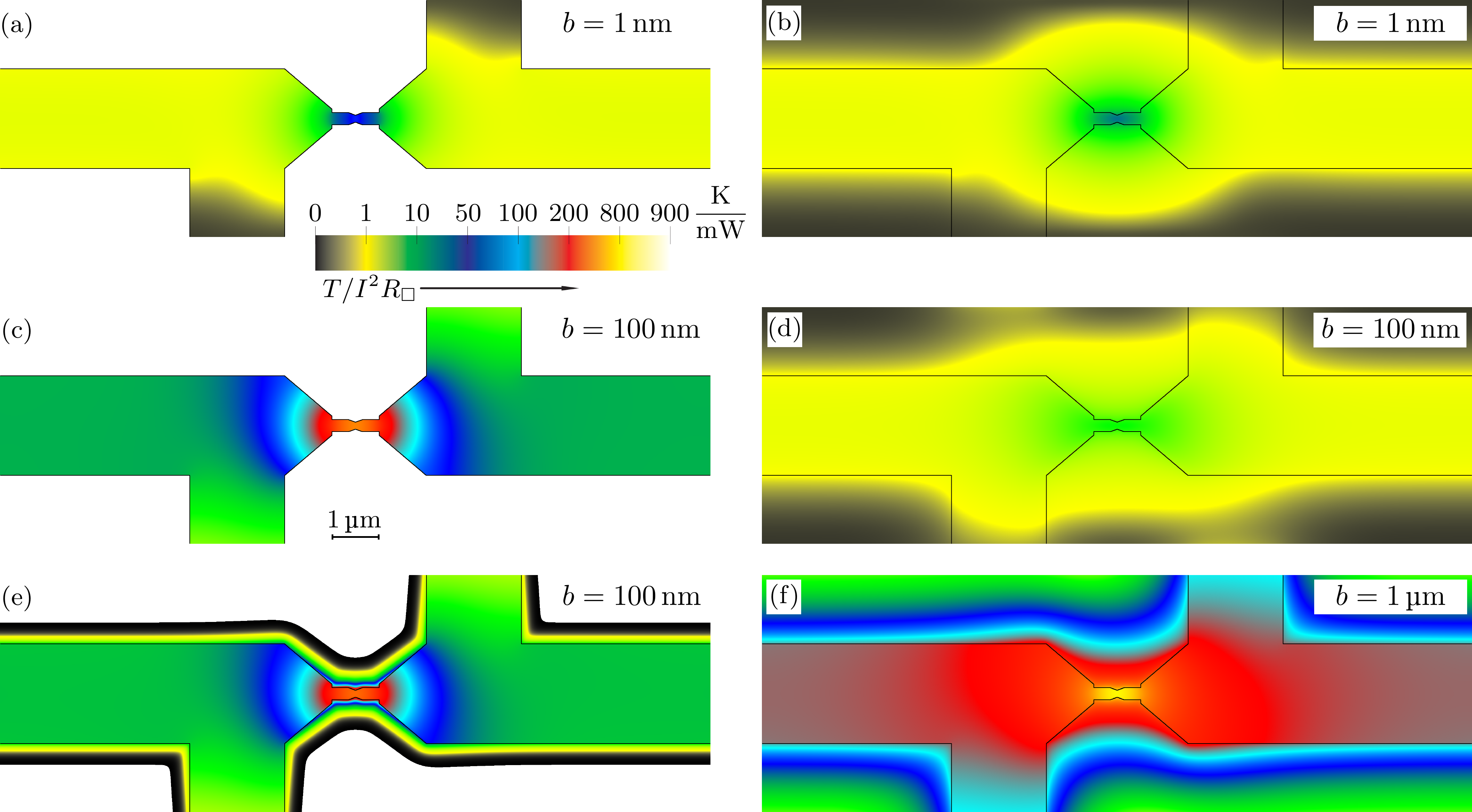
Figure 3 shows the results for nm, nm, and µm. Obviously, the temperatures of substrate and metallic structure follow each other closely for very thin barriers [see Fig. 3 (a) and (b)]. For thicker barriers the asymptotic temperature in the leads can easily reach values that exceed the maximum temperature for thin barriers [compare Fig. 3 (a) and (c), calculated with Approx. I, i. e., a 3d heat relaxation in the substrate and a vertical laminar flow in the barrier]. The temperature is maximal at the center of the wire as expected. A typical value for the sheet resistance is Ω, so that mW at around mA. For this current a moderate temperature rise of K results at the center of the narrow wire, if the barrier thickness nm. For nm the temperature rises already by K. The substrate temperature below the leads, however, does not change significantly for thicker barriers due to the fact that the substrate underneath long leads is heated by the power density independent of barrier thickness [compare Fig. 3 (b) and (d)]. For Ω we get a marginal warming by about 1.6 K at mA. Furthermore, substrate heating below the center of the wire is reduced with increasing . Between nm and nm the maximum temperature rise in the substrate drops from about 30 K to 10 K. This is a rather low temperature increase as compared to the rise in the metallic structure, i. e., Approx. II is a better choice for nm. Figure 3 (e) displays the temperature profile in the plain defined by the interface between the barrier and metal film calculated in the framework of Approx. II, i. e. evaluating the 3d heat relaxation in the barrier, while the substrate is assumed to remain cold. Approximations I and II lead to similar results at nm as can be judged by inspecting Fig. 3 (c) and (e). Barrier heating is restricted mainly to the regions underneath the metallic structure for nm with a small halo only. At larger [see Fig. 3 (f)], however, the area of the barrier with a significant temperature rise has a considerably larger extent. Nevertheless, a pronounced maximum of the temperature in the central spot of the structure remains the dominant feature.111Our model does not take into account the effect of radiation cooling because the latter is negligible. The radiation losses are bounded by µW/µm2 ( is the Stefan-Boltzmann constant and K the melting point of gold) and thus several orders of magnitude smaller than the power carried by heat transport in case of significant heating.
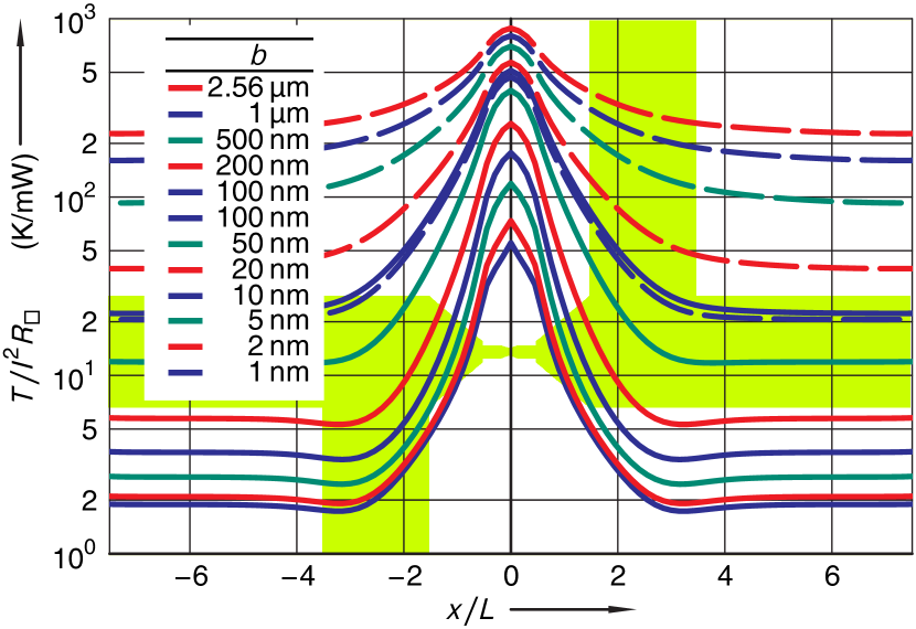
Data for further values of are summarized in Fig. 4, where the temperature profile along the central axis is displayed. The successive rise of the asymptotic lead temperature with for is the most prominent feature in this figure. Furthermore, one can observe that the ratio between the maximum temperature in the center and is strongly reduced with increasing . For nm results of Approx. I and II are included. Both approximations yield similar results at this thickness, with slightly lower values of for Approx. II due to the more efficient cooling resulting from the temperature halo around the metallic structure visible in Fig. 3 (e).
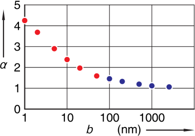
In a well accepted approximationHo and Kwok (1989), the amount of gold pushed in the anode direction is proportional to both the current density and the self-diffusivity of the metallic cores. The latter has a strong temperature dependence described over a wide range by an Arrhenius lawMehrer (1990) (for self-diffusion data on Au see, e. g., Refs. Gupta, 1973a, b; Gupta and Asai, 1974; McLean and Hirth, 1968). No matter whether electromgration is dominated by diffusion in the bulk, along grain boundaries, or at the surface, a sizeable effect sufficient for the deliberate formation of voids requires elevated temperatures. As a rule of thumb, should be at least half the melting temperature , in which case electromigration along grain boundaries is the dominant atomic flux mechanism. The effect of electromigration is much stronger just below melting and is then in general dominated by flux within the bulk. However, for a controlled process of gap formation the melting point must not be exceeded. In Fig. 5 (a) we plot as a function of , where are the maximal values of the curves in Fig. 4 at , where the temperature in the metallic structure is highest. If we fix the temperature at a value well below the melting point (let’s say at K for gold) directly gives a safe current limit for the specific structure. This safe current limit is considerably reduced when is increased as shown in 5 (a). For a native oxide barrier of nm and Ω a current of almost mA can be tolerated. For the thermally grown oxide layer of our experiments (nm) the safe current limit is by a factor of four smaller. This makes controlled electromigration considerably more difficult. The feedback loop as implemented by us and othersHoffmann et al. (2008) uses a resistance change to judge the appropriate current density. This procedure however might lead to current densities that exceed the limit set by the melting point of gold.
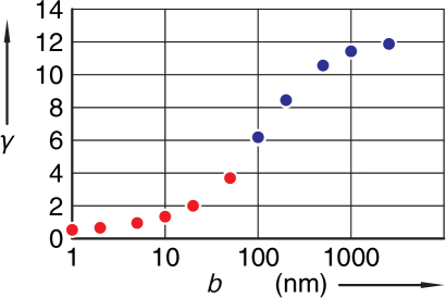
It is instructive to compare the size of the first term in Eq. (1), i. e., the heat transport in the metallic structure, to the size of the right-hand side of the same equation, i. e., the heat flow to the substrate. This is done in Fig. 5 (b) for the central point of the structure where the temperature for a given current is highest. The ratio
of these two terms is considerably smaller than for nm, i. e., the center of the structure is efficiently cooled via the substrate. For larger , however, rises quickly indicating that the coupling to the substrate becomes increasingly inefficient and cooling has to rely on the heat flow along the metallic leads. The barrier thickness at which this decoupling sets in is expected to be reduced with decreasing width of the notch in the center. Thus, if void formation by electromigration occurs and the current path through a narrowing constriction, temperature is dominated more and more by the heat flow along the structure. This leads to an even stronger tendency towards melting which has to be counteracted by increasingly careful settings in the feedback-control loop and necessitates good thermal coupling from the beginning. In summary, our analysis gives clear evidence why controlled electromigation on thick oxide barriers is more likely to fail.
Figure 5 (c) displays the ratio of the temperatures at the wire end (i. e., at the crossover from the narrow region to the funnel-shaped parts of the leads) and at the center, as a function of . Ideally, the temperature peaks so strongly at the center that electromigration acts only there with reasonable strength. This is difficult to achieve, though. Figure 5 (b) indicates that an optimal barrier thickness exists at which . This factor-of-two reduction of the temperature is not sufficient as demonstrated by the experimental result presented in Fig. 1 (a). As indicated in the inset of Fig. 2 the current density peaks not only at the notch in the center but at concave corners as well. Electromigration leads to material flux in regions of high current density. The formation of voids or hillocks, in turn, requires some kind of inhomogeneity that causes a divergence of material flux. Such an inhomogeneity might be simply due to the statistical distribution of grains comprising the metallic structure, but regions of high temperature gradient lead for sure to a divergence in atomic flux as the delivery of material from cold regions is less efficient than delivery of material to the hotter parts. In the structure studied here the temperature gradient is large at the wire end and vanishes in the center where the notch is located. In the latter position material transport tends to be balanced and thus the wire cross-section does not change to first order. Only at the corner at the cathode end void formation is favored.
(a)
 (b) (c)
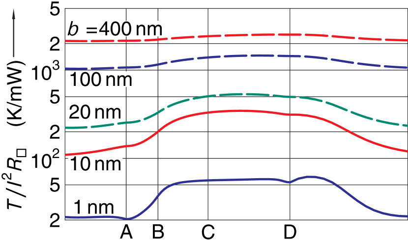
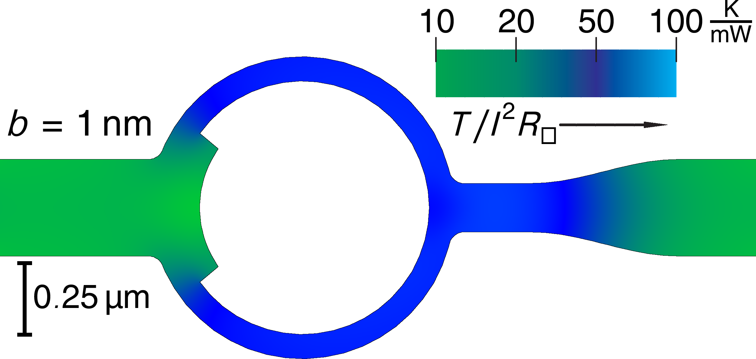
Figure 5 (d) compares calculations for two different structures, namely the four-probe configuration with source and drain contacts and two voltage probes studied so far, and a two-probe configuration with no voltage probes. Clearly the temperature is reduced in the vicinity of the current-free voltage probes. However, their cooling effect is confined to a small region whose extent is set by the relaxation parameter in Eq. 4. The design of cooling fins would require to place them within a distance set by . For the model parameter used in our calculations nm, 930 nm, and 2.9 µm for nm, 100 nm, and 1 µm, respectively. The voltage probes in our test structure are within the range of the central notch for µm, only. Consequently, the temperature is slightly reduced in the center in this case as can be seen in Fig. 5 (d). Note, however, that the temperature in the center of the structure is peaking on top of the asymptotic temperature and this temperature scales quadratically with , the width of the source and drain leads. Thus, a stronger reduction can be obtained by making the leads as wide as possible.
To demonstrate the application of our numerical simulations for the optimization of the sample layout with respect to control over the location where gap formation sets in, we design a structure in which the current path branches into a loop (see Fig. 6). The final goal with this specific structure is to produce two gaps, one in each loop arm. If bridged by molecules, such a sample could be used to test for the quantum coherence of electron transport through molecules by measuring the magnetoconductance. Coherence would lead to the appearance of periodic oscillation of the conductance in response to the magnetic flux penetrating the area between the loop armsWebb et al. (1985). In the design of Fig. 6 (a) we try to avoid unintentional current density enhancements by rounding all concave corners. A step in the width of the current path is introduced only at two positions. The inset in the ring center of Fig. 6 (a) demonstrates that this leads to a considerable current-density enhancement at singular points. At the same time we would like to have a large temperature gradient at this location. To this end we make the current path twice as narrow on the anode side of the ring structure and thus the power density by a factor of four larger. The investigation of coherent transport requires a high aspect ratio of the open area between the loop arms and the part of the ring area covered by metal. For this reason, the step in the ring width is placed close to the cathode side of the structure. Figure 6 (c) shows the result of Approx. I for a thin barrier (nm). The temperature changes abruptly at the transition from the wide to the narrow part of the ring thus making the concave corner at this position a preferred starting point for void formation. In Fig. 6 (b) we display the temperature profile along the path drawn as a blue line in Fig. 6 (a) for various barrier thicknesses. The temperature gradient is large at point B for a thin barrier as intended. The temperature reaches to first approximation almost constant values to the left of point A and between point C and D for nm on account of a short relaxation parameter nm. With increasing thickness , however, Joule heating leads to a more evenly distributed temperature due to the rise in . As a result, the temperature gradient at point B gets more and more shallow making the tendency to void formation at the corner weaker. Still, electromigration is boosted by the current-density rise at this location which is thus distinguished from the rest of the structure. Nevertheless, the statistical nature of grain boundaries easily marks different locations along the line from B to D where void formation might start. Hence, it is not clear from the outset that the corner close to point B will win for larger . This again stresses that reliable void formation is favored by good thermal coupling via a thin barrier to a substrate of high thermal conductance.
V Conclusion
In this paper we have presented experimental results showing that nanogap formation by electromigration depends crucially on the thickness of an insulating barrier between the metallic structure and a thermally well conducting substrate. We have developed a numerical model which explains these findings by considering the strength of thermal coupling of the metallic structure to the substrate. Only for thin barriers is cooling by heat flow to the substrate efficient, while for thick barriers the temperature is governed only by heat flow along the leads connecting the microstructures to regions of lower current densities. Thus, only thin barriers allow the large current densities required for void formation on a reasonable time scale without melting large parts of the structure by Joule heating. Therefore, good thermal coupling is an important prerequisite for well controlled electromigration. On the other hand, thin barriers are not always an option in practice. The native oxides on silicon wafers have been reported to be as thin as nm. While such a thin barrier yields a good thermal contact it bears the risk of undesirable electrical leakage currents through the substrate. For a reliable electrical insulation of the structure a barrier of several 100 nm thickness is mandatory. In our model calculation we considered cooling the structure by coupling it to a cold substrate. If electromigration has to be performed in vacuum for some reason, this might be the only option. In this case a thermally well conducting insulator is required. Another option would be to operate electromigration in a controlled atmosphere. We have, e. g., performed electromigration experiments in the gas phase above the liquid level of a Helium dewar. The structure heated by a high current density leads to convection of the cold gas which in turn gives rise to an efficient heat release. The yield of sufficiently small nanogaps considerably increased in this case even on thick SiO2 barriers. Whether the resulting gaps are clean and not contaminated with metallic nano-clusters is an open question at this momentHouck et al. (2005); Heersche et al. (2006); van der Zant et al. (2006).
Besides efficient heat release, a good layout design is needed to predefine the position of void formation. The latter starts preferably at positions where high current densities meet large temperature gradients. It is thus advisable not to place the intended gap position in high symmetry points of the layout where temperature gradients are expected to vanish but to mark it with sharp corners which can be utilized for a considerable current density enhancement.
Acknowledgements.
We acknowledge useful discussions with Regina Hoffmann, Dominik Stöffler, and Michael Marz.*
Appendix A Calculation of
We calculate by discrete cosine transform (DCT) on a cube of cells (N=1024 turns out to be sufficient) with the basic approach
| (8) |
where and the arguments of the cosine functions are chosen to assure , , , and . Together with the discrete version of the Laplace equation,
| (9) |
this describes a single source of unit strength at . is the discrete version of the Laplace operator , , and for all other combinations of the indices. From Eq. (9) one gets
| (10) |
where is the DCT of defined with the same arguments in the cosine functions as in Eq. (8). Thus the calculation of involves two DCT operations and normalization of the intermediate result according to Eq. (10). The index enters into the calculation via the definition of , where is the discretization size in the finite-difference method. For Approx. I we need to know . We approximate it by setting , which is sufficiently accurate due to the asymptotic nature of the analytical solution.
References
- Ho and Kwok (1989) P. S. Ho and T. Kwok, Rep. Prog. Phys. 52, 301 (1989).
- Park et al. (1999) H. Park, A. K. L. Lim, A. P. Alivisatos, J. Park, and P. L. McEuen, Appl. Phys. Lett. 75, 301 (1999).
- Park et al. (2000) H. Park, J. Park, A. K. L. Lim, E. H. Anderson, A. P. Alivisatos, and P. L. McEuen, Nature 407, 57 (2000).
- Houck et al. (2005) A. A. Houck, J. Labaziewicz, E. K. Chan, J. A. Folk, and I. L. Chuang, Nano Lett. 5, 1685 (2005).
- Heersche et al. (2006) H. B. Heersche, Z. de Groot, J. A. Folk, , L. P. Kouwenhoven, and H. S. J. van der Zant, Phys. Rev. Lett. 96, 017205 (2006).
- van der Zant et al. (2006) H. S. J. van der Zant, Y.-V. Kervennic, M. Poot, K. O’Neill, Z. de Groot, J. M. Thijssen, H. B. Heersche, N. Stuhr-Hansen, T. Bjørnholm, D. Vanmaekelbergh, C. A. van Walree, and L. W. Jenneskens, Faraday Discuss. 131, 347 (2006).
- Strachan et al. (2005) D. R. Strachan, D. E. Smith, D. E. Johnston, T.-H. Park, M. J. Therien, D. A. Bonnell, and A. T. Johnston, Appl. Phys. Lett. 86, 043109 (2005).
- Esen and Fuhrer (2005) G. Esen and M. S. Fuhrer, Appl. Phys. Lett. 87, 263101 (2005).
- Strachan et al. (2007) D. R. Strachan, D. E. Smith, M. D. Fischbein, D. E. Johnston, B. S. Guiton, M. Drndić, D. A. Bonnell, and A. T. Johnston, Nano Lett. 6, 441 (2007).
- Hoffmann et al. (2008) R. Hoffmann, D. Weissenberger, J. Hawecker, and D. Stöffler, Appl. Phys. Lett. 93, 043118 (2008).
- Blech and Meieran (1967) I. A. Blech and E. S. Meieran, J. Appl. Phys. 11, 263 (1967).
- Blech and Meieran (1969) I. A. Blech and E. S. Meieran, Appl. Phys. Lett. 40, 485 (1969).
- Heersche et al. (2007) H. B. Heersche, G. Lientschnig, K. O’Neill, H. S. J. van der Zant, and H. Zandbergen, Appl. Phys. Lett. 91, 072107 (2007).
- Press et al. (2007) W. H. Press, S. A. Teukolsky, V. W. T., and B. P. Flannery, Numerical Recipies (Cambridge University Press, 2007).
- Jackson (1999) J. D. Jackson, Classical Electrodynamics (John Wiley & Sons, New York, 1999).
- Durkan (2007) C. Durkan, Current at the Nanoscale (Imperial College Press, London, 2007).
- Powell et al. (1966) R. W. Powell, C. Y. Ho, and P. E. Liley, NSRDS-NBS 8, Thermal Conductivity of Selected Materials, Tech. Rep. (National Bureau of Standards, 1966).
- Glassbrenner and Slack (1964) C. J. Glassbrenner and G. A. Slack, Phys. Rev. 134, A1058 (1964).
- Kleiner et al. (1996) M. B. Kleiner, S. A. Kühn, and W. Weber, IEEE Trans. on Electr. Dev. 43, 1602 (1996).
- Note (1) Our model does not take into account the effect of radiation cooling because the latter is negligible. The radiation losses are bounded by µW/µm2 ( is the Stefan-Boltzmann constant and K the melting point of gold) and thus several orders of magnitude smaller than the power carried by heat transport in case of significant heating.
- Mehrer (1990) H. Mehrer, ed., Diffusion in solid metalls and alloys, Landolt-Börnstein, New Series, Group III, Vol. 26 (Springer, Berlin, Heidelberg, NewYork, 1990).
- Gupta (1973a) D. Gupta, J. Appl. Phys. 44, 4455 (1973a).
- Gupta (1973b) D. Gupta, Phys. Rev. B 7, 586 (1973b).
- Gupta and Asai (1974) D. Gupta and K. W. Asai, Thin Solid Films 22, 121 (1974).
- McLean and Hirth (1968) M. McLean and J. P. Hirth, Surface Science 11, 177 (1968).
- Webb et al. (1985) R. A. Webb, S. Washburn, C. P. Umbach, and R. B. Laibowitz, Phys. Rev. Lett. 54, 2696 (1985).