Optical addressing of an individual erbium ion in silicon
The detection of electron spins associated with single defects in solids is a critical operation for a range of quantum information and measurement applications currently under developmentMorello et al. (2010); Fuechsle et al. (2012); Pla et al. (2012); Gaebel et al. (2006); Jiang et al. (2009); Togan et al. (2010); Maze et al. (2008); Morton et al. (2011); Zwanenburg et al. (2012). To date, it has only been accomplished for two centres in crystalline solids: phosphorus in silicon using electrical readout based on a single electron transistor (SET)Morello et al. (2010) and nitrogen-vacancy centres in diamond using optical readoutGaebel et al. (2006); Togan et al. (2010). A spin readout fidelity of about 90% has been demonstrated with both electrical readoutMorello et al. (2010) and optical readoutRobledo et al. (2011); Neumann et al. (2010), however, the thermal limitations of the electrical readout and the poor photon collection efficiency of the optical readout hinder achieving the high fidelity required for quantum information applications. Here we demonstrate a hybrid approach using optical excitation to change the charge state of the defect centre in a silicon-based SET, conditional on its spin state, and then detecting this change electrically. The optical frequency addressing in high spectral resolution conquers the thermal broadening limitation of the previous electrical readout and charge sensing avoids the difficulties of efficient photon collection. This is done with erbium in silicon and has the potential to enable new architectures for quantum information processing devices and to dramatically increase the range of defect centres that can be exploited. Further, the efficient electrical detection of the optical excitation of single sites in silicon is a major step in developing an interconnect between silicon and optical based quantum computing technologies.
The potential for a hybrid optical/electrical single-spin readout was recently established by Steger et al., revealing long nuclear spin coherence time with an ensemble of P ions in highly purified 28SiSteger et al. (2012). The readout of the spin ensemble was demonstrated by detecting the photocurrent generated when the excitonic transition at 1,078 nm associated with the P ions was excited. In the current work we demonstrate single-site detection by electrically detecting the optical excitation of the 4I15/2 - 4I13/2 transition of single Er ions implanted into silicon, resolving both electronic Zeeman and hyperfine structure. The efficient readout required for single-site detection is achieved by measuring the photo-induced change in the site’s charge state using a SET, rather than detecting the associated photocurrent.
Erbium’s large electronic magnetic moment of its ground state, the =7/2 nuclear spin of its 167 isotope along with the coincidence of the 4I15/2 - 4I13/2 transition with the 1.5 m transmission window of silica optical fibers make Er centres appealing for quantum information applicationsKenyon (2005); Vinh et al. (2009); Bertaina et al. (2007). The few existing studies in samples with a high concentration of Er have shown 0.1 s nuclear spin relaxation timeBaldit et al. (2010) and 100 s electron spin dephasing timeBertaina et al. (2007). Single-site detection grants access to low Er densities where one expects drastically enhanced coherence times in analogy to the impressive recent development for P in SiSteger et al. (2012). The low emission rate from optically excited rare-earth ions such as Er3+ makes pure optical detection of single sites challengingKenyon (2005); Vinh et al. (2009). Recently though, the optical detection of a single rare-earth ion was demonstrated in a Pr-doped YAG nano-crystalKolesov et al. (2012). The technique employed, involved the 2-step excitation of the ion to a high lying 5d-electron state and detecting the resultant emissionKolesov et al. (2012). It was conducted at room temperature and exhibited low detection efficiency and low frequency resolution making state readout not feasible.
The 4I15/2 - 4I13/2 transition is between states within the inner 4f-electron shell of the Er3+ ion, which is well shielded from the surrounding lattice by filled outer shells, resulting in narrow spectral linewidths and the potential for high resolution frequency addressing. At liquid helium temperatures homogeneous linewidths as narrow as 50 Hz have been observed for the transition in Er3+:Y2SiO5Sun et al. (2002). Prior to the present work there have not been any sub-inhomogeneous studies conducted on optical transition in Er centres in silicon. The observed lifetime of emission of 2 ms from the 4I13/2 state for Er3+ ions in silicon implies a minimum linewidth of 150 HzPriolo et al. (1998).
The resonant photoionization of individual Er3+ ions is studied in an Er-implanted SET (Fig. 1a), which works as a charge sensor. The 4I15/2 - 4I13/2 transition of an Er3+ ion has a relatively high probability, when a laser is tuned to its resonant wavelength, and the Er3+ ion could be further ionized due to a second-photon process or an Auger process. The charge displacement induced by an ionization event simultaneously leads to a change in the tunnelling current of the SET. To get a high sensitivity, the SET is biased close to the degeneracy point between two charge states, i.e. at the edge of one Coulomb peak (Fig. 1b). Accordingly, the transconductance is large, and a small charge displacement in the sensitive region will lead to a significant change in the tunnelling currentPioda et al. (2011); Hanson et al. (2007). The photoionization of individual Er3+ ions leads to a significant change in tunnelling current (Fig. 1b). The 4I15/2 - 4I13/2 transition of each Er3+ ion has a specific resonant photon energy, so individual Er3+ ions are distinguished by the resonant photon energy. When the laser is tuned to a non-resonant wavelength, the tunnelling current mainly stays at the background level as shown in Fig. 1c. In contrast, when the laser is tuned to a resonant wavelength of an Er3+ ion, the photoionization of the Er3+ ion leads to a rise in the tunnelling current, and then the current drops back due to its neutralization, contributing a two-level current-time trace (Fig. 1d), which suggests only one single Er3+ ion is ionized (details in Methods). Figure 1e shows a photoionization spectrum of a single Er3+ ion. Current-time traces are recorded at a series of photon energies, and then the histogram showing the distribution of current in time is plotted as a function of the photon energy detuning. The colour in Fig. 1e represents the time () during which the current stays within one bin, and a 0.02-nA bin size is used for all the analysis.
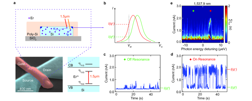
As shown in Fig. 1a, the SET has a Si channel wrapped with the gate. The SET is biased below the threshold voltage, so that the current tunnels through the corner regions of the Si channelSellier et al. (2007). Consequently, the charge sensor is more sensitive to the Er3+ ions which are closer to the corner regions in the channel, and different Er3+ ions have different capacitive coupling leading to different detection sensitivity. The change in current (Fig. 1b-d) accords with the loss of an electron, indicating that it’s due to the ionization of the Er centre, whereas the gain of an electron will lead to a shift opposite to that in Fig. 1b. The small fluctuations in current, which we attribute to the trap states in the insulating layer or the oxide layer with weak capacitive couplingTettamanzi et al. (2011), can be suppressed by a proper anneal before the device fabrication. The readout efficiency is mainly limited by the efficiency of the excitation from the 4I13/2 excited state into the conduction band, which can be increased to close to 100%, by increasing the intensity of the light used to drive this final ionization step. We observe resonances via the photoionization spectroscopy mostly between 1,535 nm and 1,539 nm, which is consistent with the 4I15/2 - 4I13/2 transition of Er3+ ions in siliconKenyon (2005); Vinh et al. (2009).
In the next experiment, we study the Zeeman effect of individual Er3+ ions, as the Zeeman effect is an essential tool to determine the site symmetry of Er centres. Er3+ ions tend to take 3+ valence characteristic of the Si lattice, so the 4f electrons of Er3+ ions have the ground state of 4I15/2 and the first excited state of 4I13/2Kenyon (2005). The degeneracy is lifted by the crystal field, so that each state splits into several levels depending on the symmetry of the Er centreKenyon (2005). The transition between the lowest level of 4I15/2 and the lowest level of 4I13/2 is responsible for the strong emission band around 1.54 m, and the Zeeman splitting of those two levels in the case of double degeneracy is shown in Fig. 2a. The doublet states can be described by an effective spin =1/2, and the Zeeman interaction has the form: =, where is the electronic Bohr magneton, is the magnetic field, and is the -factor matrixGuillot-Noël et al. (2006). The Zeeman splitting energy of the higher (lower) energy doublet is proportional to (). As shown in Fig. 2a, the energy difference between the two =1 (=0) transitions can be described by , where is the -factor difference. In this study, we measured the Zeeman splitting of 4 spectrally isolated Er resonances, and observed the -factor difference from 1.6 to 10.8.
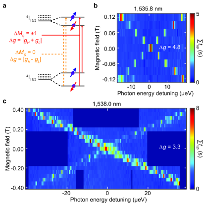
Figure 2b,c shows the Zeeman splitting of Er3+ ions. Current-time traces are taken at a series of photon energies and magnetic fields, and each pixel in Fig. 2b,c represents one current-time trace. When an Er3+ ion is ionized, the current will exceed a certain threshold, which is determined by the background current fluctuation under non-resonant illumination. For each current-time trace, the time (), during which the current exceeds the threshold, is integrated and gives the values () plotted in Fig. 2b,c. As shown in Fig. 2b, the resonance shows up at the photon energy detuning of 1 eV at zero magnetic field, and starts to split into two diagonal arms with increasing magnetic field. It is due to the Zeeman effect of one individual Er3+ ion, with . Similarly, the Zeeman splitting of the resonance around 1,538.0 nm is studied as shown in Fig. 2c, and the rectangular regions denoted by the darkest blue colour are not scanned. There appear to be two resonances with similar resonant wavelengths and the same -factor difference () but with different signal intensity. This could be due to two individual Er3+ ions with the same site symmetry but with different capacitive coupling. Furthermore, the Zeeman splitting of the resonance around 1,538.0 nm shows polarization dependence. As shown in Fig. 2c, the diagonal arm is weaker than the anti-diagonal one. By modifying the polarization of the light entering the cryostat, the diagonal arm was tuned to be stronger than the anti-diagonal one. The site symmetry of individual Er centres can be determined with the polarization dependence and a rotating magnetic field measurement. Spin selective excitation even for degenerate spin states can be achieved with the maximum contrast of the polarization dependence, which allows spin readout without a magnetic field.
The hyperfine structure is of great interest as the nuclear spin has long coherence times for quantum information storageSteger et al. (2012); Hedges et al. (2010); Simmons et al. (2011). In addition, it is a strong evidence for distinguishing between different ions as well as other defects. Erbium has six stable isotopes, among which only 167Er has a nonzero nuclear spin of =7/2, leading to eight nuclear spin states. At high magnetic field, the hyperfine interaction can be treated as a perturbation of the Zeeman effectSmith and Unsworth (1965), so each electron spin state will split into eight sublevels due to the hyperfine interaction (Fig. 3a). At low magnetic field, the hyperfine interaction is comparable to the Zeeman effect, so the sublevels will mixMcAuslan et al. (2012).
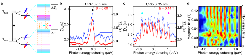
In order to investigate the hyperfine structure of 167Er3+ ions, we implanted 167Er and 168Er with zero nuclear spin as control ions. We first study the photoionization spectrum of an Er3+ control ion with zero nuclear spin. The integrated time () is plotted as a function of the photon energy detuning, as indicated by the blue dashed line in Fig. 3b. The same spectral asymmetry as that in Fig. 1e is observed. We attribute the asymmetry to the correlation between the Stark shift of the 4I15/2 - 4I13/2 resonance and a broadening of the Coulomb peak, both of which are sensitive to fluctuating electric fields in the channel. The fluctuating field is attributed to the laser excitation of trap states in or near the channel. Since we directly observe the effect on the Coulomb peak it is possible to remove part of this broadening of the peak. After applying this correction (details in Methods), a minimum FWHM spectral width of 50 neV is observed as indicated by the red solid line in Fig. 3c. To significantly reduce the linewidth further it will be necessary to reduce the density of trap states. As well as the electric field induced shifts the line is expected to be broadened through magnetic interactions with 29Si up to tens of neV and with paramagnetic centres in the device. It is expected from analogy with observations in Er3+:Y2SiO5Sun et al. (2002) that applying a large magnetic field will suppress this broadening mechanism.
In the following, we show the hyperfine structure of one 167Er3+ ion. As shown in Fig. 3c, the photoionization spectrum taken at high magnetic field ( T), reveals eight resonant peaks with the photon energy difference of about 0.2 eV between each other. The high spectral resolution allows the nuclear spin readout with potential for single-shot readout and manipulating the nuclear spin states. As the addressability doesn’t rely on a specific magnetic field, the photoionization spectra are measured at a series of magnetic fields, as shown in Fig. 3d. The Zeeman shift is subtracted to show evolution of the hyperfine interaction. At high magnetic field, eight significant peaks are observed all through (0.08 T 0.14 T), as the hyperfine interaction can be treated as a perturbation of the Zeeman effect. At low magnetic field, multiple resonances show up (-0.04 T 0.06 T), revealing the mixing of the hyperfine sublevels, since the hyperfine interaction is comparable to the Zeeman effect.
The eight significant peaks, representing the eight different nuclear spin states of 167Er, demonstrate that the resonances are due to the 167Er3+ ion rather than other ions or defects. These eight hyperfine peaks (Fig. 3c) correspond to the allowed transitions (=0) preserving the nuclear spin states, but it’s still a question whether they are due to the =0 or =1 transitions. As shown in Fig. 3a, we attribute them to the =0 transitions for two reasons. First, the energy difference between the two most distant hyperfine peaks is only about 1.7 eV (Fig. 3c), which is much smaller than the typical splitting energy of the =1 transitions of Er3+ ions. The electron paramagnetic resonance measurements of 167Er3+ ions in crystals show a splitting energy () of about 30 eVYang et al. (2009); Bertaina et al. (2007), which corresponds to the =1 transitions. Second, a ninth peak shows up beyond the region between the two most distant peaks (at the photon energy detuning of -1.1 eV in Fig. 3c). The ninth peak is much weaker than the eight peaks but still recognizable, which we attribute to a not-allowed transition. The energy of the not-allowed transitions (=1) of Er3+ ions can exceed the region between the two most distant peaks of the allowed transitions, only in the case of the =0 transitions. Consequently, the eight significant peaks are attributed to the =0 transitions, and the splitting energy is expressed as =1.7 eV.
Hybrid optical/electrical access to single spins of individual ions in a nano-transistor has been demonstrated, which is applicable for other defects in solids. Specifically, with an Er-implanted SET the photoionization spectroscopy allows real-time observation of single optical excitation events avoiding the bottleneck of photon collection. Furthermore, high-resolution optical frequency addressing circumvents the limitations due to thermal broadening in earlier electrical detection of impurity spinsMorello et al. (2010). Our findings open the way to optically address and manipulate the electron and nuclear spin states of an individual defect in a solid beyond the nitrogen-vacancy centre in diamond. In addition, this hybrid optical/electrical technique boosts the microstructural study of ions in a semiconductor to a single-site level, including microscopic aspects, electrical and optical activity, etc.
An approach that combines dopant ions (e.g. Er, P) with quantum optical control and semiconductor fabrication technologies represents an attractive platform to realize a scalable quantum computation and communication architecture. Such a system could consist of individual ions inside a ring cavity coupled with each other via photons, and nearby charge-sensing devices used to read out the spin states of individual ions and to control the coupling between ions by Stark tuning. The ring cavities can be connected by optical waveguides, which enable quantum information transfer between individual ions in different ring cavities. Here we demonstrated the first step towards such a system, i.e. optical addressing of individual ions, and further improvement can be made by reducing the observed linewidth as discussed previously. However, there are essential questions to be addressed in the future, such as electron and nuclear spin coherence times of Er (P) ions, the influence of photoionization on nuclear spin coherence, and spin-photon entanglement.
METHOD SUMMARY
The devices are fabricated with the same technique as the previous studyLansbergen et al. (2008). After complete device fabrication, an Er:O co-implantation (dose ratio 1:6 ) is performed with the implantation energy of 400 keV and 55 keV, respectively. There should be approximately 30-40 Er ions in the sensitive region of one Coulomb peak. Under the erbium implantation conditions we used, the beam is estimated to have been composed of 70-80% 168Er and 20-30% 167Er. The devices are then annealed at 700∘C in N2 for 10 minutes to remove the implantation damage and to initiate the formation of Er centres. All the measurements are carried out in a liquid helium cryostat at 4.2 K. The laser beam, with 4-5 mW optical power, goes through a single-mode fiber and irradiates the sample with a diameter of about 1 mm. In the initial phase of the experiments (Figs. 1 and 2), a commercial tunable laser with an external cavity is used. To keep a high precision, we set one centred wavelength with the motor-actuator, and sweep the wavelength around the centred wavelength with the piezo-actuator. In the high-resolution experiments (Fig. 3), the wavelength of another laser is stabilized to about 0.01 pm, and a wavelength meter is used to compensate the thermal drift.
Acknowledgements We thank R. Ahlefeldt, J. Bartholomew, R. Elliman, N. Manson and A. Morello for discussions. We also thank M. Hedges and T. Lucas for their help in the initial phase of the experiments. The devices were fabricated by N. Collaert and S. Biesemans (IMEC). The work was financially supported by the ARC Centre of Excellence for Quantum Computation and Communication Technology (CE110001027), and the Future Fellowships (FT100100589 and FT110100919).
Author Contribution N.S. and J.C.M. designed and performed the implantation. C.M.Y., M.J.S. and S.R. designed and conducted the experiments. C.M.Y., M.R. and G.G.d.B. carried out the experiments. All the authors contributed to analysing the results and writing the paper. Correspondence and requests for materials should be addressed to S.R. (s.rogge@unsw.edu.au).
References
- Morello et al. (2010) A. Morello, J. J. Pla, F. A. Zwanenburg, K. W. Chan, K. Y. Tan, H. Huebl, M. Möttönen, C. D. Nugroho, C. Yang, J. A. van Donkelaar, A. D. C. Alves, D. N. Jamieson, C. C. Escott, L. C. L. Hollenberg, R. G. Clark, and A. S. Dzurak, Nature 467, 687 (2010).
- Fuechsle et al. (2012) M. Fuechsle, J. A. Miwa, S. Mahapatra, H. Ryu, S. Lee, O. Warschkow, L. C. L. Hollenberg, G. Klimeck, and M. Y. Simmons, Nature Nanotechnology 7, 242 (2012).
- Pla et al. (2012) J. J. Pla, K. Y. Tan, J. P. Dehollain, W. H. Lim, J. J. L. Morton, D. N. Jamieson, A. S. Dzurak, and A. Morello, Nature 489, 541 (2012).
- Gaebel et al. (2006) T. Gaebel, M. Domhan, I. Popa, C. Wittmann, P. Neumann, F. Jelezko, J. R. Rabeau, N. Stavrias, A. D. Greentree, S. Prawer, J. Meijer, J. Twamley, P. R. Hemmer, and J. Wrachtrup, Nature Physics 2, 408 (2006).
- Jiang et al. (2009) L. Jiang, J. S. Hodges, J. R. Maze, P. Maurer, J. M. Taylor, D. G. Cory, P. R. Hemmer, R. L. Walsworth, A. Yacoby, A. S. Zibrov, and M. D. Lukin, Science 326, 267 (2009).
- Togan et al. (2010) E. Togan, Y. Chu, A. S. Trifonov, L. Jiang, J. Maze, L. Childress, M. V. G. Dutt, A. S. Sørensen, P. R. Hemmer, A. S. Zibrov, and M. D. Lukin, Nature 466, 730 (2010).
- Maze et al. (2008) J. R. Maze, P. L. Stanwix, J. S. Hodges, S. Hong, J. M. Taylor, P. Cappellaro, L. Jiang, M. V. G. Dutt, E. Togan, A. S. Zibrov, A. Yacoby, R. L. Walsworth, and M. D. Lukin, Nature 455, 644 (2008).
- Morton et al. (2011) J. J. L. Morton, D. R. McCamey, M. A. Eriksson, and S. A. Lyon, Nature 479, 345 (2011).
- Zwanenburg et al. (2012) F. A. Zwanenburg, A. S. Dzurak, A. Morello, M. Y. Simmons, L. C. Hollenberg, G. Klimeck, S. Rogge, S. N. Coppersmith, and M. A. Eriksson, arXiv preprint arXiv:1206.5202 (2012).
- Robledo et al. (2011) L. Robledo, L. Childress, H. Bernien, B. Hensen, P. F. A. Alkemade, and R. Hanson, Nature 477, 574 (2011).
- Neumann et al. (2010) P. Neumann, J. Beck, M. Steiner, F. Rempp, H. Fedder, P. R. Hemmer, J. Wrachtrup, and F. Jelezko, Science 329, 542 (2010).
- Steger et al. (2012) M. Steger, K. Saeedi, M. L. W. Thewalt, J. J. L. Morton, H. Riemann, N. V. Abrosimov, P. Becker, and H.-J. Pohl, Science 336, 1280 (2012).
- Kenyon (2005) A. J. Kenyon, Semiconductor science and technology 20, R65 (2005).
- Vinh et al. (2009) N. Q. Vinh, N. N. Ha, and T. Gregorkiewicz, Proceedings of the IEEE 97, 1269 (2009).
- Bertaina et al. (2007) S. Bertaina, S. Gambarelli, A. Tkachuk, I. N. Kurkin, B. Malkin, A. Stepanov, and B. Barbara, Nature Nanotechnology 2, 39 (2007).
- Baldit et al. (2010) E. Baldit, K. Bencheikh, P. Monnier, S. Briaudeau, J. A. Levenson, V. Crozatier, I. Lorgeré, F. Bretenaker, J. L. Le Gouët, and O. Guillot-Noël, Physical Review B 81, 144303 (2010).
- Kolesov et al. (2012) R. Kolesov, K. Xia, R. Reuter, R. Stöhr, A. Zappe, J. Meijer, P. Hemmer, and J. Wrachtrup, Nature Communications 3, 1029 (2012).
- Sun et al. (2002) Y. Sun, C. W. Thiel, R. L. Cone, R. W. Equall, and R. L. Hutcheson, Journal of luminescence 98, 281–287 (2002).
- Priolo et al. (1998) F. Priolo, G. Franzò, S. Coffa, and A. Carnera, Physical Review B 57, 4443 (1998).
- Pioda et al. (2011) A. Pioda, E. Totoki, H. Kiyama, T. Fujita, G. Allison, T. Asayama, A. Oiwa, and S. Tarucha, Physical review letters 106, 146804 (2011).
- Hanson et al. (2007) R. Hanson, J. R. Petta, S. Tarucha, and L. M. K. Vandersypen, Reviews of Modern Physics 79, 1217 (2007).
- Sellier et al. (2007) H. Sellier, G. P. Lansbergen, J. Caro, S. Rogge, N. Collaert, I. Ferain, M. Jurczak, and S. Biesemans, Applied Physics Letters 90, 073502 (2007).
- Tettamanzi et al. (2011) G. C. Tettamanzi, A. Paul, S. Lee, S. R. Mehrotra, N. Collaert, S. Biesemans, G. Klimeck, and S. Rogge, IEEE Electron Device Letters 32, 440 (2011).
- Guillot-Noël et al. (2006) O. Guillot-Noël, P. Goldner, Y. Le Du, E. Baldit, P. Monnier, and K. Bencheikh, Physical Review B 74, 214409 (2006).
- Hedges et al. (2010) M. P. Hedges, J. J. Longdell, Y. Li, and M. J. Sellars, Nature 465, 1052 (2010).
- Simmons et al. (2011) S. Simmons, R. M. Brown, H. Riemann, N. V. Abrosimov, P. Becker, H.-J. Pohl, M. L. Thewalt, K. M. Itoh, and J. J. Morton, Nature 470, 69 (2011).
- Smith and Unsworth (1965) K. F. Smith and P. J. Unsworth, Proceedings of the Physical Society 86, 1249 (1965).
- McAuslan et al. (2012) D. L. McAuslan, J. G. Bartholomew, M. J. Sellars, and J. J. Longdell, Physical Review A 85, 032339 (2012).
- Yang et al. (2009) S. Yang, S. M. Evans, L. E. Halliburton, G. A. Slack, S. B. Schujman, K. E. Morgan, R. T. Bondokov, and S. G. Mueller, Journal of Applied Physics 105, 023714 (2009).
- Lansbergen et al. (2008) G. P. Lansbergen, R. Rahman, C. J. Wellard, I. Woo, J. Caro, N. Collaert, S. Biesemans, G. Klimeck, L. C. L. Hollenberg, and S. Rogge, Nature Physics 4, 656 (2008).
METHODS
Details of the devices. The devices used in this study are n-p-n field-effect transistors with a polycrystalline silicon gate wrapped around the p-type silicon channel separated by the gate dielectric. The p-type channel has a boron doping of 1018 cm-3. After complete device fabrication, an Er:O co-implantation is performed with the implantation energy of 400 keV and 55 keV and the ion fluence of cm-2 and cm-2, respectively. This leads to an Er:O dose ratio of about 1:6 in the channel region. Under the erbium implantation conditions we used, the beam is estimated to have been composed of 70-80% 168Er and 20-30% 167Er. The presence of both oxygen impuritiesKenyon (2005) and boron impurities31 is known to enhance the luminescence of the Er3+ ions in silicon. The 700∘C post-implantation anneal is within the thermal processing window for Er centre activation in silicon31.
In the experiments, the device is biased below the threshold voltage, and only the corner regions of the silicon channel go into inversionSellier et al. (2007). A peak of the - curve is due to the Coulomb blockade in one of the two corner regions, where the current flows. The sensitive region is defined as the region, in which one elementary charge change can be detected, with taking the current noise and the transconductance of the Coulomb peak into account. The sensitive region of one Coulomb peak is estimated to be the corresponding channel-corner region with a dimension of nm (length width height) for the device shown in Fig. 1a. Simulations of the ion implantation based on SRIM32 show that there should be approximately 30-40 Er ions in the sensitive region of one Coulomb peak.
Experimental details and data analysis. All the measurements are carried out in a liquid helium cryostat at 4.2 K. The laser beam, with 4-5 mW optical power, goes through a single-mode fiber and irradiates the sample with a diameter of about 1 mm. In the initial phase of the experiments (Figs. 1 and 2), a commercial tunable laser with an external cavity is used. To keep a high precision, we set one centred wavelength with the motor-actuator, and sweep the wavelength around the centred wavelength with the piezo-actuator. The current-time traces in Fig. 1c and Fig. 1d taken at two different photon energies are consistent with the photoionization spectrum as indicated by the green and red diamonds in Fig. 1e, respectively. For instance, the current mainly stays at the background level (0.4 nA) at the photon energy detuning of -5 eV, while the current jumps between two levels (1.8 nA and 0.4 nA) at the photon energy detuning of 4 eV. It is worth to note that the two-level trace (Fig. 1d) suggests only one single Er3+ ion is ionized. Multiple ions with different capacitive coupling will lead to a current-time trace with more than two levels, while two ions with the same capacitive coupling will lead to a current-time trace with three levels once they are simultaneously ionized. We attribute the charge displacement to the ionization of an Er3+ ion rather than the charge fluctuations of the trap states, based on the observation that all the Er3+ ions that we observed contribute to a shift of the Coulomb peak towards lower gate voltage. In the high-resolution experiments (Fig. 3), the wavelength of another laser is stabilized to about 0.01 pm, and a wavelength meter is used to compensate the thermal drift. The asymmetry as well as part of the broadening of the resonant peak is removed by adding an photon energy offset to the data, and then the time, during which the current exceeds the threshold, is integrated and gives the values plotted as the red solid line in Fig. 3b,c. In comparison, the red solid line with removing the broadening shows smaller widths and less noise than the blue dashed line without removing the broadening, nevertheless, the resonances in the latter are still clearly visible, as shown in Fig. 3b,c.
References
31 J. Michel, J. L. Benton, R. F. Ferrante, D. C. Jacobson, D. J. Eaglesham, E. A. Fitzgerald, Y.-H. Xie, J. M. Poate, and L. C. Kimerling, Journal of Applied Physics 70, 2672 (1991)
32 J. F. Ziegler, M. Ziegler, and J. Biersack, Nuclear Instruments and Methods in Physics Research Section B: Beam Interactions with Materials and Atoms 268, 1818 (2010).