Edge states and topological properties of electrons on the bismuth on silicon surface with giant spin-orbit coupling
Abstract
We derive a model of localized edge states in the finite width strip for two-dimensional electron gas formed in the hybrid system of bismuth monolayer deposited on the silicon interface and described by the nearly-free electron model with giant spin-orbit splitting. The edge states have the energy dispersion in the bulk energy gap with the Dirac-like linear dependence on the quasimomentum and the spin polarization coupled to the direction of propagation, demonstrating the properties of topological insulator. The topological stability of edge states is confirmed by the calculations of the invariant taken from the structure of the Pfaffian for the time reversal operator for the filled bulk bands in the surface Brillouin zone which is shown to have a stable number of zeros with the variations of material parameters. The proposed properties of the edge states may support future advances in experimental and technological applications of this new material in nanoelectronics and spintronics.
pacs:
73.20.At, 75.70.Tj, 85.75.-dI Introduction
During the last decade an increasing attention is given to a new class of structures called topological insulators (TI) with promising characteristics both in fundamental aspects of their physics and possible applications in nanoelectronics, spintronics, and fabrication of new magnetic, optical and information processing devices.KaneRMP ; QiZhangRMP ; Moore2010 ; Culcer ; Qi2008 The principal features of TI include the presence of time-reversal (TR) invariance in the system where the propagating edge states may exist being localized near the boundary of host material and have the dispersion relation which is linear near the origin of their quasimomentum (Dirac-like structure), corresponding to the energies belonging to the insulating gap of the bulk material. The spin of such states is firmly attached to the direction of propagation along the edge, making them protected against backscattering due to the TR invariance which leads to effective cancelling of two scattered states with opposite possible directions of the spin flip which accompanies such backscattering. The existence of such edge states have been shown in numerous theoretical models of TI, and also in the experiments. The materials included graphene,KaneMele HgTe/CdTe quantum wells,BHZ ; Koenig ; Zhou ; Krueckl2011 bismuth thin films,Murakami quantum wiresHuber2011 , nanocontacts or bilayers,Sabater2013 the LiAuSe and KHgSb compounds,ZhangChadov as well as general two-dimensional models of paramagnetic semiconductorsQiWuZhang , the silicene,Ezawa ; Drummond2012 and the topological nodal semimetals.Burkov2011 Another 2D TI has been predicted in the inverted Type II semiconductor InAs/GaSb quantum well,Liu2008 and observed experimentally in the contribution of the edge modes to the electron transport.Knez2011 Also a lot of studies has been devoted to the general properties of two- and three-dimensional models of TI with certain symmetries,FuKane ; FuKaneMele ; Fukui2007 ; Fu ; Drummond2012 ; Hou2011 ; Levin2011 ; Li2012 where four topological invariants have been found in 3D TI instead of the single invariant in 2D TI.FuKaneMele ; KaneRMP ; QiZhangRMP
Recently a general group theoretical analysis has been made for the links between the geometry of the Bravais lattice and the properties of TI.Slager It should be mentioned that the symmetry arguments have always played a significant role in classifying the systems as trivial or topologically protected against external perturbations.KaneMele ; FuKane ; Slager ; Doucot ; Schnyder2008 ; Mirlin2010 The time-reversal property of spin-1/2 particles in such systems can be described by the presence of time reversal invariance (i.e. without the magnetic impurities or external magnetic field) and the absence of the spin rotational invariance, here the time reversal operator is given by , where is the complex conjugation operator and is the second Pauli matrix. According to the general symmetry considerations,Schnyder2008 ; Mirlin2010 this means the class AII symmetry for the Hamiltonian for which the so called topological order is possible for two- and three-dimensional systems, forming the basis for the TI properties.
The studies of three-dimensional materials were mostly focused on the , or KaneRMP ; QiZhangRMP ; Hsieh2008 ; Miyamoto2012 ; Nechaev2013 where also the edge states were constructed explicitly in several models of the finite-size geometry.Linder ; Lu Another important issue is the effects of impurities and disorder on the band structure and topological stability in TI. It is known that TI are robust against weak disorder or the potentials produces by non-magnetic impurities, KaneMele ; FuKane ; ShengHaldane2006 while the presence of magnetic impurities may lead to the hybridization of the insulator atomic orbitals and the magnetic material orbitals, producing the strong modification to metallic or non-metallic nature of the states and their spin polarization. Caprara2012 Even for non-magnetic impurities it has been shown recently that the formation of impurity bands within the energy gap at strong doping of the bulk material may lead to their mixing with the edge states of TI, modifying their structure, however keeping the order and the topological stability.Lee2013
It can be seen that although the features of the TI are very general and describe a truly novel state of matter, the number of different materials demonstrating these features is currently quite limited. So, it is of interest to find new materials and compounds where possible manifestations of TI may be present, for both fundamental aspects and applied purposes. It is needful also to understand which properties of the edge states are common for different systems, and which are special, and how all of them are related to the bulk quantum states in a specific model.
Here we consider a model of edge states and connect their properties to the topological characteristics of the host material for a new candidate for the class of topological insulators: the two-dimensional electron gas (2DEG) in a material with strong spin-orbit coupling (SOC) formed at the interface of the monolayer of bismuth deposited on the silicon. This material is characterized by a giant SOC splitting which was predicted or observed experimentally also in a number of metal films or the combined materials of the ”metal on semiconductor” type, Hirahara2006 ; Hirahara2007 ; Grioni2008 ; Dil2008 ; Gierz2009 ; Azpiroz2011 ; FPG and recently described theoretically.FPG ; JETP Its huge spin splitting together with the hexagonal type of the lattice creates a certain potential of manifestation of the TI properties, since the spin-resolved bands may evolve into spin-resolved edge states, and the hexagonal type of the lattice is favorable for the TI to exist.Slager
The properties of 2DEG at the Bi/Si interface have been studied experimentally with the help of angle-resolved photoemission spectroscopy (ARPES) FPG ; Hirahara2006 ; Hirahara2007 ; Hirahara2007b ; Grioni2008 ; Dil2008 ; Gierz2009 ; Bian2009 ; Sakamoto2009 applied also to other materials. It was found that this material represents an example of nowadays widely studied class of materials with large (up to eV) SOC spin splitting of their energy bands, which can be formed in various compound materials or heterostructures of the ”metal on semiconductor” type. It is known for many years that SOC plays an important role in formation of the TI properties,Sheng1996 including the localization effects of Rashba SOC combined with electron-electron interaction,Strom2010 the Dirac-cone surface states in Basak2011 and ,Niesner2012 or ,Protogenov and ,Zhang2009 the topological phasesChern2010 ; Ruegg2012 and quantum spin Hall phase in honeycomb lattice,Bercioux2011 the ultracold Fermi gases,Sau2011 the spin Hall effect in graphene,Dyrdal2012 and the Kondo insulator effects.Dzero2012 ; Craco2012
Various materials with strong SOC have been a subject of intensive studies throughout recent years, including the structures of Bi deposited on Si-Ge substrates,Miwa2005 the Pb on Si structure,Dil2008 the trilayer Bi-Ag-Si system,Grioni2008 the structures with monolayer of Pb atoms covering the Ge surface,Yaji2010 or the Pb on Ge structures.Sherman2012 One can mention also new types of triple bulk compounds with strong SOC like ,Okamoto BiTeI or other bismuth tellurohalides,Ishizaka2011 ; Gnezdilov2013 ; Chulkov or recently discussed material.Rasche2013
In the present paper we adopt the nearly-free model of two-dimensional bulk states in Bi/Si developed earlierFPG and applied in the extended form in our previous paper for the description of spin polarization, charge conductance and optical properties of this promising materialJETP for the calculation of the 1D edge states of the electrons on the Bi/Si interface in the finite strip geometry. We obtain both the explicit form of the edge wavefunctions and the edge energy spectrum, calculate their spin polarization, and link the possible topological stability of their properties to the topological invariant studied by the analysis of the time reversal matrix elements behavior in the Brillouin zone.KaneRMP ; QiZhangRMP ; Qi2008 ; KaneMele ; FuKane ; Fukui2007 The results of our paper are of interest for expanding the knowledge of new materials with the topologically protected properties where the SOC plays a significant role, making them suitable for further applications in spintronics as stable current-carrying and spin-carrying channels.
The paper is organized as following. In Sec.II we briefly described the nearly free-electron (NFE) model of 2D bulk states at Bi/Si interface, and derive a model for the 1D edge states for the electrons in the finite strip geometry. We calculate their spectrum, wavefunctions, and spin polarization. In Sec.III we reinforce our findings on the edge state stability by considering the topological band properties of the 2D bulk states in Bi/Si, and find the results supporting the presence of the TI phase. Our conclusions are given is Sec.IV.
II Model for bulk states and edge states
II.1 Bulk states
Our model for the 1D edge states is based on the 2D NFE model for the bulk states of 2DEG formed at the interface of the trimer Bi/Si(111) structureFPG developed for the description of the spectrum near the M-point of the BZ, and later extended for the modeling of the electron states in the whole BZ.JETP This model was compared with its expansion containing the anisotropic terms in the NFE model as well as with an empirical tight-binding model.FPG While the details of band structure and the quality of reproduction of experimental ARPES data on energy bands in Bi/Si vary from model to model, the simple NFE model allows to reconstruct the main properties of spin split bands including the magnitude of splitting, the energy gap, and the spin polarization. It also has a major advantage of a straightforward derivation of the edge states in a finite strip geometry, as we shall see below.
In this model, the Hamiltonian for the 2DEG in the BZ of plane is written as a sum of free-electron term with SOC,
| (1) |
, corresponding to the Rashba paraboloid centered in the Gamma point of the hexagonal BZ, and the lattice potential represented via the spatial Fourier expansion with reciprocal space vectors as
| (2) |
The parameters of both the and are fitted as to provide the best correspondence between the model and the structure of the bands near the Fermi level experimentally known from ARPES measurements.Grioni2008 ; Dil2008 ; Gierz2009 ; FPG The typical valuesFPG ; JETP are , and eV, although they should be treated as fitting parameters rather than measured material constants, and in the present paper we shall consider their variations in the range of eV for and for . The structure of reciprocal space vectors connecting the equivalent Gamma points in the hexagonal lattice is shown in Fig.1a. In the model originally proposedFPG only the vectors were included in order to described the states near the M point, and later we expanded this modelJETP with vectors for the description of the states in the whole BZ. The parameters of the hexagonal lattice in Fig.1a are and .
The Bloch eigenstate of the Hamiltonian is a two-component spinor which can be constructed under the NFE approximation in the following form:
| (3) |
where the Rashba eigenstates have the form of free electron states with the quasimomentum shifted by the vector , see Fig.1a, and
| (4) |
The sign corresponds to two eigenvalues for Rashba energy spectrum .
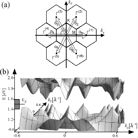
In Fig.1b we plot the fragment of the energy spectrum of 2DEG at the Bi/Si(111) surface in the NFE model corresponding to the bulk band gap (labeled by at the left part of the figure) of around eV between the bands where the Fermi level is located, reported to be above the second spin split band.FPG The Fermi level position in the bulk gap where the gapped structure of the electron spectrum is produced by the hexagonal lattice with potential (2) creates the possibility of the edge states formation with energies in this gap, and, as we shall see below, makes the system a possible new candidate for the topological insulator class. The large metallic-like values of electron energy and SOC amplitude present for the 2DEG in this system make it promising for the consideration in transport and optical experiments where the disorder, collision and thermal broadening prevent the application of conventional semiconductors. It should be noted that the discussed properties of the band structure for Bi/Si 2DEG are obtained in the framework of one specific model with a set of parameters chosen for the best fit to experimental data. Thus, it may be modified in the future when more insight will be gained on the properties of Bi/Si or other similar compounds. Still, we shall see below that the qualitative and topologically described features of the electron states studied within this model are robust against the significant variations of the model parameters, which is an indication of certain intrinsic and stable properties of the system.
II.2 Edge states
We now turn our attention to the construction of the model for the edge states localized at the opposite edges of the finite strip formed in the 2DEG. We can start with the strip geometry where the electrons are confined along the direction in the strip and with conventional assumption of the hard-wall boundary conditions .Koenig ; Zhou ; Krueckl2011 ; Linder ; Lu
First, the spectrum of edge states can be found by solving the eigenstate problem with the requirement of exponential dependence across the strip direction . It can be done by starting from the bulk Hamiltonian and replacing the quasimomentum component in the direction of confinement by the pure imaginary variable describing the inverse localization depth corresponding to the localized states which means in our case the substitution . It should be mentioned that in general can be complex with imaginary part corresponding to the oscillations of the edge wavefunctions on top of the exponential decayKoenig ; Linder while in other models Zhou is taken purely real, like in our system. The reason for purely real in our model of edge states is the narrow bulk gap formed in the bulk spectrum originating from Hamiltonian (1) with strong Rashba SOC. If one adds more real nonzero wavevector components by adding the imaginary part to , then the resulting energy increase will push the edge states out of the bulk gap, making them unsuitable for the TI phase.
The eigenfunctions of this Hamiltonian can be constructed in the same nearly free-electron approximation as the bulk states (3), and have the following form:
| (5) | |||
| (6) |
The spinors can be obtained from (4) with the substitution , which results in a real number under the Arg function, giving us
| (7) |
The summation in (6) is over the 1D lattice in the reciprocal space which corresponds not to 2D hexagonal but the 1D simple lattice along the direction formed by the vectors and from Fig.1a, with the real space period period where is the length of the vector. The state (6) remains to be Bloch function along with the conventional translational property , while along the confinement direction the wavefunctions are exponents . If we solve the Schrödinger equation for our model of 2DEG at Bi/Si interface with the substitution (without considering the specific boundary conditions at this stage), the spectrum of edge states will be obtained as a function of two parameters . If there are eigenstates with energies corresponding to the gap in the bulk spectrum, one can be interested in them as in potential candidates for the edge states with topological protection.
The wavefunction satisfying the boundary conditions on a single edge and having the specific energy in the bulk gap has the form of linear combination of (6) with different localization lengths corresponding to the given energy :
| (8) |
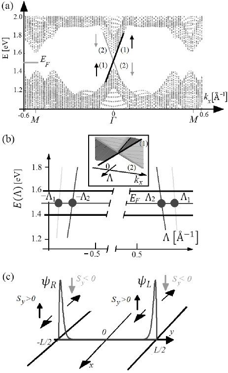
If the edge is represented by another and more smoothly rising potential differing from the hard wall, or more sophisticated boundary condition is chosen, the edge wavefunction is expected to be modified mainly in the small vicinity of the edge where a decaying tail can be formed. Since this modification would not affect seriously the global shape of the edge state and the main localization parameter, as well as the primary property of their possible topological stability induced by the presence of the topological invariant for the bulk states,we shall proceed with the simple hard wall condition introduced above. We have found that in our model the edge states indeed exist in the gap of the bulk spectrum, and their dependence on the parameter is shown in Fig.2(a) as two linear dispersion curves (1) and (2) crossing the bulk gap for typical value of inverse localization length , together with the bulk spectrum plotted vs for all values of in the 2D Brillouin zone shown in Fig.1a. The joint dependence on both and for the energy of the edge states is shown as 3D plot in the inset for Fig.2b. The two spin-resolved branches of energy are shaded differently (branch (1) is dark gray and branch (2) is light gray) there with respect to their spin projection . In Fig.2(a) we also plot the mean values of the only nonvanishing spin component for the edge states which are coupled to their direction of motion along the strip. The spin-up states are moving to the right with the group velocity while the spin-down states are moving to the left (), shown in the same grayscale level with corresponding branches of the edge spectrum.
An important feature of the edge state spectrum is the presence of two roots for each value of energy for a given , i.e. the equation has two pairs of solutions for the left and right edge of the strip, respectively, as it is shown in Fig.2b for the dependence of the energy on at . Such structure of energy eigenvalues is the direct consequence of the relative proximity of two branches of Rashba spectrum present in the basis for the Hamiltonian which can be also seen for the bulk spectrum in Fig.1b. This feature allows one to construct the edge states satisfying the boundary conditions for the band of energies located in the bulk energy gap, as it is done in various models of edge states in TI.Koenig ; Zhou ; Linder ; Lu
The specific boundary conditions are applied to the general form of the edge state (8). The two wavefunctions for the given energy satisfying the boundary condition on the left edge of the strip (when facing in the forward direction of the axis) and decaying into the strip have the form (8) and can be constructed explicitly by the following superposition of the states (6):
| (9) |
| (10) |
where the normalization condition is implied in . Correspondingly, the localized wavefunctions for the right edge can be written as
| (11) |
| (12) |
All the edge states (9),(10) and (11),(12) have different spinor parts due to the different value of parameter , and in general may describe different spin polarization. It should be noted that their spin properties are described by the mean value of spin calculated for the edge state which itself is not labeled by the spin quantum number, as typical in the systems with SOC where the spin operator does not commute with the Hamiltonian. Still, since for the 1D edge states their direction of propagation is strongly coupled to the sign of the mean spin polarization and the edge subband index, one can link these two properties together and describe the edge states as having a definite spin mean value.
An example of the edge wavefunctions is shown in Fig.2(c) for the energy of the edge state equal to the Fermi level inside the bulk gap eV and for the strip width nm. One can see that the edge states are well-localized at the corresponding edge of the strip on the length of about 1 nm if the corresponding bulk topological invariant is nontrivial, as it is discussed in the next section. The arrows indicate the direction of propagation and the spin of each state in pair (9),(10) and (11),(12). The direction of the propagation of two chiral states on the one edge in our model is the same as on the other edge , which can be explained by to the strong Rashba SOC in our system leading, among other things, to the dominant polarization of the states moving in the direction. Here the non-compensated total spin can be accumulated if the population of right-moving and left-moving electrons is unbalanced, for example, by external electric field , as it happens in various models with current-induced spin polarization both in conventional materials with strong SOC and in TI,KS which is also can be expected for the edge states shown in Fig.2(c).
The form of spin polarization shown in Fig.2(a),(c) creates a positive expectation about their topological stability for the charge transport against the scattering on non-magnetic impurities which do not violate the TR symmetry, if supported by the analysis of the topological properties of the bulk states indicating the presence of a nontrivial topological invariant. If we consider the backscattering, then it is clear from Fig.2(c) that the change of the propagation direction will lead to the spin flip, and such reversal cancels the reflected waves and extinguishes the backscattering.KaneRMP ; QiZhangRMP This is consistent with the arguments of the topological stability of such edge states as the participants of charge transport, which is the required property of a system to become a topological insulator. We shall see below in Sec.III that our assumption about the 2DEG on the Bi/Si interface as a possible TI is supported further by the analysis of the topological properties of 2D bulk states.
III Topological properties of bulk states
It is known from the general theory that the stability of edge states is guaranteed by certain topological properties of the bulk states. In particular, the system can be a TI if an integer called invariant is different from zero.KaneRMP ; QiZhangRMP ; KaneMele ; FuKane There are several ways for calculation of this invariant, and here we shall use the method proposed by Kane and Mele KaneMele which links the index to the zeros of the Pfaffian for the interband matrix elements of the time reversal operator between the occupied bands, which has the form for the spin-1/2 particles, where is the complex conjugation operator. If we have only two lowest bands occupied which is the case of 2DEG in Bi/Si 2DEG, then the Pfaffian is equal to the single off-diagonal matrix element between the Bloch functions in the occupied bands and ,
| (13) |
The topological considerations provide a convenient form of using the definition (13) for the task of finding new material demonstrating the properties of TI. Namely, if for the hexagonal BZ the -dependent function has pairs of zeros in the corners of the BZ (or, depending on the overall symmetry, on the lines inside the BZ), then the system demonstrates the properties of TI.KaneMele ; Murakami ; FuKane There is an extensive discussion of the invariant properties related to the TI including another definition of it where the matrix elements of TR operator are calculated between the states with opposite wavevectors and and the TI is determined by its properties not in the entire BZ but at discrete set of ”time reversal invariant points” like or points. The detailed discussion and all relevant mathematical connections between different approaches on the calculation of invariant can be found in the literature.KaneRMP ; QiZhangRMP ; FuKane ; Schnyder2008 ; Ryu2007 ; Fukui2007 ; Roy2009 ; Yu2011
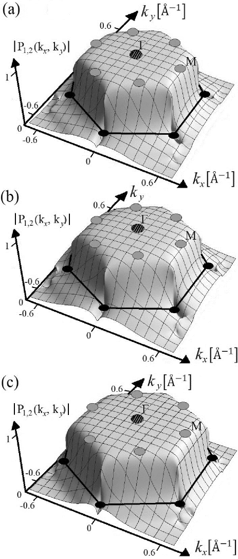
In Fig.3a we plot the absolute value of the Pfaffian (13) in the hexagonal BZ for the 2DEG on the Bi/Si interface for the same basic set of model parameters as were used for calculations of the bulk spectrum in Fig.1b. In order to see the possible changes in the index with the variation of the system parameters, in Fig.3b,c we plot for two other sets of parameters: in Fig.3b the amplitude of the periodic potential is increased compared to the basic case shown in Fig.1b, eV and the amplitude of Rashba SOC is the same, . In Fig.3c the periodic potential amplitude is the same as in Fig.3a, eV, but the Rashba coupling amplitude is decreased, . It is clearly seen for all cases that the Pfaffian has zeros in the corners of the BZ where the visible zeros are shown as black circles which border is shown schematically, while in the TR-invariant and points shown as shaded and light gray circles, respectively. There are three pairs of zeros for which indicates that the invariant is odd, thus classifying the 2DEG at the Bi/Si interface as a topological insulator with the protected edge states.KaneRMP ; QiZhangRMP ; KaneMele ; FuKane The presentation of the structure of Pfaffian in Fig.3 in the whole BZ is useful in determining the areas where the states of different bands belong to the ”even” or ”odd” subspace relatively to the action of the time reversal operator , in accordance with the classification proposed by Kane and Mele.KaneMele In our case shown in Fig.3 we see that the major part of the BZ corresponds to the states belonging to the even subspace with , however by approaching the borders of the BZ the value of is modified significantly, and in the corners we arrive to the odd subspace where , so the property of TI is present.
One can also see in Fig.3 that the variations of material parameters do not change significantly the topological properties of the Pfaffians which all have the same qualitative features with at the TR-invariant and points and with three pairs of zeros for in the corners of the BZ. The depth of the parameter variation present in three parts of Fig.3 is rather big and reaches which covers a wide range of possible experimental and technological fabrication of the 2DEG at the Bi/Si interface. Still, the absolute values of Pfaffians shown in Fig.3 look very similar to each other which indicates their qualitative topological nature being the key for discovering new examples of topological insulators. The method of mutual analysis of chiral edge states and topological bulk properties used in our calculations can be applied to other materials and structures.
IV Conclusions
We have derived a model for the one-dimensional edge states for the electrons on the bismuth on silicon interface in the finite strip geometry. Based on the bulk nearly free-electron model, their energy dispersion was obtained inside the bulk gap being linear in the quasimomentum. The spin polarization of edge states is linked to the direction of propagation along the given edge which provides topological stability of these chiral modes. The topological stability of edge states was confirmed by the structure of the interband matrix element for the time reversal operator which was shown to be stable against the large variations of material parameters. The results of the paper may be of interest both for the development of the topological insulator theory by providing a novel example of the material belonging to this class, and also for the development of new spintronics and nanoelectronics devices with stable transport and operating at room temperature.
Acknowledgements
The authors are grateful to V.Ya Demikhovskii, A.M. Satanin, A.P. Protogenov, G.M. Maximova, V.A. Burdov and A.A. Konakov for helpful discussions. The work is supported by the Russian Foundation for Basic Research (Grants No. 13-02-00717a, 13-02-00784a).
References
- (1) M.Z. Hasan and C.L. Kane, Rev. Mod. Phys. 82, 3045 (2010).
- (2) X.-L. Qi and S.-C. Zhang, Rev. Mod. Phys. 83, 1057 (2011).
- (3) J.E. Moore, Nature 464, 194 (2010).
- (4) D. Culcer, Physica E 44, 860 (2012).
- (5) X.-L. Qi, T.L. Hughes, and S.-C. Zhang, Phys. Rev. B 78, 195424 (2008).
- (6) C.L. Kane and E.J. Mele, Phys. Rev. Lett. 95, 146802 (2005); 95, 226801 (2005).
- (7) B.A. Bernevig, T.L. Hughes, and S.-C. Zhang, Science 314, 1757 (2006).
- (8) M. König, H. Buhmann, L.W. Molenkamp, T.L. Hughes, C.-X. Liu, X.-L. Qi, and S-C. Zhang, J. Phys. Soc. Jpn 77, 031007 (2008).
- (9) B. Zhou, H.-Z. Lu, R.-L. Chu, S.-Q. Shen, and Q. Niu, Phys. Rev. Lett. 101, 246807 (2008).
- (10) V. Krueckl and K. Richter, Phys. Rev. Lett. 107, 086803 (2011).
- (11) S. Murakami, Phys. Rev. Lett. 97, 236805 (2006); M. Wada, S. Murakami, F. Freimuth, and G. Bihlmayer, Phys. Rev. B 83, 121310 (R) (2011).
- (12) T.E. Huber, A. Adeyeye, A. Nikolaeva, L. Konopko, R.C. Johnson, and M.J. Graf, Phys. Rev. B 83, 235414 (2011).
- (13) J.G. Rodrigo, A. García-Martín, J.J. Sáenz, and S. Vieira, Phys. Rev. Lett. 88, 246801 (2002); C. Sabater, D. Gosálbez-Martínez, J. Fernández-Rossier, J.G. Rodrigo, C. Untiedt, and J.J. Palacios, arxiv:1304.0934 (2013).
- (14) H.-J. Zhang, S. Chadov, L. Müchler, B. Yan, X.-L. Qi, J. Kübler, S.-C. Zhang, and C. Felser, Phys. Rev. Lett. 106, 156402 (2011).
- (15) X.-L. Qi, Y.-S. Wu, and S.-C. Zhang, Phys. Rev. B 74, 085308 (2006).
- (16) L. Fu and C.L. Kane, Phys. Rev. B 74, 195312 (2006); Phys. Rev. B 76, 045302 (2007).
- (17) L. Fu, C.L. Kane, and E.J. Mele, Phys. Rev. Lett. 98, 106803 (2007).
- (18) T. Fukui and Y. Hatsugai, Phys. Rev. B 75, 121403(R) (2007).
- (19) L. Fu, Phys. Rev. Lett. 106, 106802 (2011).
- (20) M. Ezawa, Phys. Rev. Lett. 109, 055502 (2012); Phys. Rev. B 86, 161407 (2012); Phys. Rev. Lett. 110, 026603 (2013); arXiv:1303.1245 (2013).
- (21) N.D. Drummond, V. Zólyomi, and V.I. Fal’ko, Phys. Rev. B 85, 075423 (2012).
- (22) J.-M. Hou, W.-X. Zhang, and G.-X. Wang, Phys. Rev. B 84, 075105 (2011).
- (23) M. Levin, F.J. Burnell, M. Koch-Janusz, and A. Stern, Phys. Rev. B 84, 235145 (2011).
- (24) Y. Li, X. Zhou, and C. Wu, Phys. Rev. B 85, 125122 (2012).
- (25) A.A. Burkov, M.D. Hook, and L. Balents, Phys. Rev. B 84, 235126 (2011).
- (26) C. Liu, T.L. Hughes, X.-L. Qi, K. Wang, and S.-C. Zhang, Phys. Rev. Lett. 100, 236601 (2008).
- (27) I. Knez, R.-R. Du, and G. Sullivan, Phys. Rev. Lett. 107, 136603 (2011).
- (28) R.-J. Slager, A. Meszaros, V. Juričic̀, and J. Zaanen, Nat. Physics 9, 98 (2013).
- (29) B. Douçot, M.V. Feigel’man, L.B. Ioffe, and A.S. Ioselevich, Phys. Rev. B 71, 024505 (2005).
- (30) A.P. Schnyder, S. Ryu, A. Furusaki, and A.W.W. Ludwig, Phys. Rev. B 78, 195125 (2008).
- (31) A.D. Mirlin, F. Evers, I.V. Gornyi, and P.M. Ostrovsky, Int. J. Mod. Phys. B 24, 1577 (2010).
- (32) D. Hsieh, D. Qian, L. Wray, Y. Xia, Y.S. Hor, R.J. Cava, and M.Z. Hasan, Nature (London) 452, 970 (2008).
- (33) K. Miyamoto, A. Kimura, T. Okuda, H. Miyahara, K. Kuroda, H. Namatame, M. Taniguchi, S.V. Eremeev, T.V. Menshchikova, E.V. Chulkov, K.A. Kokh, and O.E. Tereshchenko, Phys. Rev. Lett. 109, 166802 (2012).
- (34) I.A. Nechaev, R.C. Hatch, M. Bianchi, D. Guan, C. Friedrich, I. Aguilera, J.L. Mi, B.B. Iversen, S. Blügel, Ph. Hofmann, and E.V. Chulkov, Phys. Rev. B 87, 121111 (2013).
- (35) D.N. Sheng, Z.Y. Weng, L. Sheng, and F.D.M. Haldane, Phys. Rev. Lett. 97, 036808 (2006).
- (36) S. Caprara, V.V. Tugushev, P.M. Echenique, and E.V. Chulkov, Phys. Rev. B 85, 121304(R) (2012).
- (37) S.-T. Lee, S.-M. Huang, and C.-Y. Mou, arXiv:1308.4053 (2013).
- (38) J. Linder, T. Yokoyama, and A. Sudbø, Phys. Rev. B 80, 205401 (2009).
- (39) H.-Z. Lu, W.-Y. Shan, W. Yao, Q. Niu, and S.-Q. Shen, Phys. Rev. B 81, 115407 (2010).
- (40) T. Hirahara, T. Nagao, I. Matsuda, G. Bihlmayer, E.V. Chulkov, Yu.M. Koroteev, P.M. Echenique, M. Saito, and S. Hasegawa, Phys. Rev. Lett. 97, 146803 (2006).
- (41) T. Hirahara, T. Nagao, I. Matsuda, G. Bihlmayer, E.V. Chulkov, Yu.M. Koroteev, and S. Hasegawa, Phys. Rev. B 75, 035422 (2007).
- (42) E. Frantzeskakis, S. Pons, H. Mirhosseini, J. Henk, C.R. Ast, and M. Grioni, Phys. Rev. Lett. 101, 196805 (2008).
- (43) J.H. Dil, F. Meier, J. Lobo-Checa, L. Patthey, G. Bihlmayer, and J. Osterwalder, Phys. Rev. Lett. 101, 266802 (2008).
- (44) I. Gierz, T. Suzuki, E. Frantzeskakis, S. Pons,, S. Ostanin, A. Ernst, J. Henk, M. Grioni, K. Kern, and C.R. Ast, Phys. Rev. Lett. 103, 046803 (2009).
- (45) J. Ibañez-Azpiroz, A. Eiguren, and A. Bergara, Phys. Rev. B 84 125435 (2011).
- (46) E. Frantzeskakis, S. Pons, and M. Grioni, Phys. Rev. B 82, 085440 (2010).
- (47) D.V. Khomitsky, JETP 114, 738 (2012), doi:10.1134/S1063776112030156.
- (48) T. Hirahara, K. Miyamoto, I. Matsuda, T. Kadono, A. Kimura, T. Nagao, G. Bihlmayer, E.V. Chulkov, S. Qiao, K. Shimada, H. Namatame, M. Taniguchi, and S. Hasegawa, Phys. Rev. B 76, 153305 (2007).
- (49) G. Bian, T. Miller, and T.-C. Chiang, Phys. Rev. B 80, 245407 (2009).
- (50) K. Sakamoto, H. Kakuta, K. Sugawara, K. Miyamoto, A. Kimura, T. Kuzumaki, N. Ueno, E. Annese, J. Fujii, A. Kodama, T. Shishidou, H. Namatame, M. Taniguchi, T. Sato, T. Takahashi, and T. Oguchi, Phys. Rev. Lett. 103, 156801 (2009).
- (51) D.N. Sheng and Z.Y. Weng, Phys. Rev. B 54, R11070 (1996).
- (52) A. Ström, H. Johannesson, and G.I. Japaridze, Phys. Rev. Lett. 104, 256804 (2010).
- (53) S. Basak, H. Lin, L.A. Wray, S.-Y. Xu, L.Fu, M.Z. Hasan, and A. Bansil, Phys. Rev. B 84, 121401(R) (2011).
- (54) D. Niesner, Th. Fauster, S.V. Eremeev, T.V. Menshchikova, Yu.M. Koroteev, A.P. Protogenov, E.V. Chulkov, O.E. Tereshchenko, K.A. Kokh, O. Alekperov, A. Nadjafov, and N. Mamedov, Phys. Rev. B 86, 205403 (2012).
- (55) S.V. Eremeev, I.V. Silkin, T.V. Menshchikova, A.P. Protogenov, E.V. Chulkov, JETP Lett. 96, 780 (2012).
- (56) H.-J. Zhang, C.-X. Liu, X.-L. Qi, X.-Y. Deng, X. Dai, S.-C. Zhang, and Z. Fang, Phys. Rev. B 80, 085307 (2009).
- (57) G.-W. Chern, Phys. Rev. B 81, 125134 (2010).
- (58) A. Rüegg and G.A. Fiete, Phys. Rev. Lett. 108, 046401 (2012).
- (59) D. Bercioux, N. Goldman, and D.F. Urban, Phys. Rev. A 83, 023609 (2011).
- (60) J.D. Sau, R. Sensarma, S. Powell, I.B. Spielman, and S. Das Sarma, Phys. Rev. B 83, 140510(R) (2011).
- (61) A. Dyrdał and J. Barnaś, Phys. Rev. B 86, 161401 (2012).
- (62) M. Dzero, K. Sun, P. Coleman, and V. Galitski, Phys. Rev. B 85, 045130 (2012).
- (63) L. Craco and S. Leoni, Phys. Rev. B 85, 195124 (2012).
- (64) R.H. Miwa, T.M. Schmidt, and P. Venezuela, Phys. Rev. B 72, 125403 (2005); Z.-Q. Huang, F.-C. Chuang, C.-H. Hsu, Y.-T. Liu, H.-R. Chang, H. Lin, and A. Bansil, Phys. Rev. B 88, 165301 (2013).
- (65) K. Yaji, Y. Ohtsubo, S. Hatta, H. Okuyama, K. Miyamoto, T. Okuda, A. Kimura, H. Namatame, M. Taniguchi, and T. Aruga, Nat. Commun. 1:17 doi:10.1038/ncomms1016 (2010).
- (66) J. Ibañez-Azpiroz, A. Eiguren, E.Ya. Sherman, and A. Bergara, Phys. Rev. Lett. 109, 156401 (2012).
- (67) K. Okamoto, K. Kuroda, H. Miyahara, K. Miyamoto, T. Okuda, Z.S. Aliev, M.B. Babanly, I.R. Amiraslanov, K. Shimada, H. Namatame, M. Taniguchi, D.A. Samorokov, T.V. Menshchikova, E.V. Chulkov, and A. Kimura, Phys. Rev. B 86, 195304 (2012).
- (68) K. Ishizaka, M.S. Bahramy, H. Murakawa, M. Sakano, T. Shimojima, T. Sonobe, K. Koizumi, S. Shin, H. Miyahara, A. Kimura, K. Miyamoto, T. Okuda, H. Namatame, M. Taniguchi, R. Arita, N. Nagaosa, K. Kobayashi, Y. Murakami, R. Kumai, Y. Kaneko, Y. Onose, and Y. Yokura, Nat. Materials 10, 521 (2011).
- (69) V. Gnezdilov, D. Wulferding, P. Lemmens, A. Möller, P. Recher, H. Berger, R. Sankar, and F.C. Chou, arXiv:1303.4333 (2013).
- (70) S.V. Eremeev, I.A. Nechaev, Yu.M. Koroteev, P.M. Echenique, and E.V. Chulkov, Phys. Rev. Lett. 108, 246802 (2012); G. Landolt, S.V. Eremeev, Yu.M. Koroteev, B. Slomski, S. Muff, T. Neupert, M. Kobayashi, V.N. Strocov, T. Schmitt, Z.S. Aliev, M.B. Babanly, I.R. Amiraslanov, E.V. Chulkov, J. Osterwalder, and J.H. Dil, Phys. Rev. Lett. 109, 116403 (2012); S.V. Eremeev, I.A. Nechaev, E.V. Chulkov, JETP Lett. 96, 437 (2012); I.P. Rusinov, I.A. Nechaev, S.V. Eremeev, C. Friedrich, S. Blügel, and E.V. Chulkov, arXiv:1303.4987 (2013).
- (71) B. Rasche, A. Isaeva, M. Ruck, S. Borisenko, V. Zabolotnyy, B. Büchner, K. Koepernik, C. Ortix, M. Richter, and J. van den Brink, Nat. Materials, doi:10.1038/nmat3570 (2013).
- (72) P. Kleinert, V.V. Bryksin, O. Bleibaum, Phys. Rev. B 72, 195311 (2005); V.V. Bryksin and P. Kleinert, Phys. Rev. B 73, 165313 (2006); J. Wang, K.S. Chan, and D.Y. Xing, Phys. Rev. B 73, 033316 (2006); J. Li and S.-Q. Shen, Phys. Rev. B 76, 153302 (2007); D.V. Khomitsky, Phys. Rev. B 79, 205401 (2009); Ph. Jacquod, Nanotechnology 21, 274006 (2010); P. Bokes and F. Horváth, Phys. Rev. B 81, 125302 (2010); P. Schwab, R. Raimondi, and C. Gorini, Europhys. Lett. 93, 67004 (2011); D. Culcer, Phys. Rev. B 84, 235411 (2011).
- (73) S. Ryu, C. Mudry, H. Obuse, and A. Furusaki, Phys. Rev. Lett. 99, 116601 (2007).
- (74) R. Roy, Phys. Rev. B 79, 195321 (2009).
- (75) R. Yu, X.L. Qi, A. Bernevig, Z. Fang, and X. Dai, Phys. Rev. B 84, 075119 (2011).