Charge transport in pn and npn junctions of silicene
Abstract
We investigate charge transport of pn and npn junctions made from silicene, Si analogue of graphene. The conductance shows the distinct gate-voltage dependences peculiar to the topological and non-topological phases, where the topological phase transition is caused by external electric field. Namely, the conductance is suppressed in the np regime when the both sides are topological, while in the nn regime when one side is topological and the other side is non-topological. Furthermore, we find that the conductance is almost quantized to be 0, 1 and 2. Our findings will open a new way to nanoelectronics based on silicene.
pacs:
73.23.-b, 72.80.Vp,73.40.-cI Introduction
Technology fabricating one-atom thick systems has been rapidly developing since the appearance of monolayer honeycomb carbon (graphene).Novoselov et al. (2004) Recently, silicon analog of graphene (silicene) Vogt et al. (2012); Fleurence et al. (2012); Lin et al. (2012) has been synthesized and attracts much attention. The low-lying excitations of the monolayer honeycomb systems are Dirac fermions. Due to spin-orbit interaction (SOI), the Dirac fermions become massive, i.e., the energy band has a gap. These massive Dirac fermion systems lead to a quantum spin Hall (QSH) insulator, which is originally proposed in graphene.Kane and Mele (2005a, b) However, SOI of graphene is tiny so that the QSH effect in graphene has not been experimentally observed. SOI of silicene is, in contrast, thousand times larger than that of graphene,Min et al. (2006); Yao et al. (2007) which makes experimentally accessible QSH effectsLiu et al. (2011a).
Transport properties of Dirac fermions show various anomalous behaviors. A prominent feature is the Klein tunnelingKlein (1929). Graphene heterojunctions exhibit perfect transmission through the barrier at normal incidence regardless of the barrier characteristics. The origin of the Klein tunneling is the absence of the backscattering due to the pseudospin conservation.Katsnelson et al. (2006); Beenakker (2008); Ando et al. (1998) The perfect transmission is protected by time–reversal symmetry. Actually, signature of Klein tunneling has been observed in graphene.Huard et al. (2007); Shytov et al. (2008); Young and Kim (2009) The systems supporting Dirac fermions can exhibit unique charge and spin transport.Saito et al. (2007); Sonin (2009); Yokoyama et al. (2009); Bercioux and De Martino (2010); Bai et al. (2010); Ingenhoven et al. (2010); Rataj and Barnaś (2011); Bai et al. (2011a, b); Niu (2011); Guigou et al. (2011); Liu et al. (2012); Esmaeilzadeh and Ahmadi (2012); Tian et al. (2012a, b); Rothe et al. (2012); Prada and Metalidis (2013) They have a potential to provide us with new electronics and spintronics devices.
Among such Dirac fermion systems, silicene has another advantage: the band gap is controllable by applying an external electric fieldEzawa (2012a) owing to the buckling structure.Takeda and Shiraishi (1994) A bilayer graphene also has an electric-field-tunable band gapOhta et al. (2006); McCann and Fal’ko (2006); McCann (2006); Oostinga et al. (2008); Zhang et al. (2009). Silicene, differently from a bilayer graphene, shows a topological phase transition by tuning the band gap. If one applies an electric field whose energy is stronger than SOI, the topological phase transition occurs from the QSH to non-topological insulators. It is also intriguing that silicene realizes various topological insulators by exchange interaction,Ezawa (2012b) photo-irradiationEzawa (2013a) and anti-ferromagnetic order.Ezawa (2013b)
These characteristics could be useful for device applications. The most fundamental electronic device is a field-effect transistor (FET). FET made by silicene has an advantage that it has a large band gap due to SOI compared with graphene which is a zero gap semiconductor. In addition, the tunable band gap and the topological phase transition of silicene by external electric field may lead to a new feature for FETs.
Charge transport properties of a silicene nanoribbon has been studied.Ezawa (2013c) Spin transport has been also studied in a bulk silicene junction under Zeeman field.Tsai et al. (2013) On the other hand, we focus on the charge transport in the bulk silicene. In this paper, we analyze the transport properties of pn and pnp junctions made of silicene. Controlling the conductance by tuning the gate voltage, we find that i) the gate-voltage dependences of conductance in the topological and non-topological phases are quite distinct, and ii) the conductance is almost quantized to be 0, 1 and 2. The former is an evidence for the existence of the topological phase. The latter enables us to use silicene as a FET with almost quantized three values of conductance. Our results will open a new way to future nanoelectronics.
This paper is composed as follows. In Sec. II, we review the bulk properties of silicene. In Sec. III, we investigate the pn junction of silicene. First we calculate the conductance for the normal incident case with and without the Rashba interaction. Next we calculate the obliquely incident case. The conductance is almost the same but smeared compared with that of the normal incident case. In sec. IV, we investigate a pnp junction of silicene. Section V is devoted to discussions.
II Bulk properties
First, we show the bulk properties of silicene. The Hamiltonian of a silicene in the vicinity of the K and K′ points readsLiu et al. (2011a, b); Ezawa (2012a)
| (1) |
where , , and are the Pauli matrices for the spin ( and ), sublattice (A and B sites) pseudospin, and valley (K and K′ points) spaces, respectively. and denote the lattice constant and the perpendicular distance between A and B sites, respectively.
is the intrinsic SOI coupling constant that triggers the topological phase transition from the non-topological to topological insulators (See below). The sublattice-dependent Rashba SOI also appears due to the buckling structure of silicene. And also, the mass term shows up because of the buckling structure with an external electric field along the -axis. Hereafter, we set .
We start with a review of the topological phase diagram of silicene. The Dirac mass for the K point () in the bulk silicene is given by
| (2) |
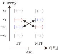
The system is a topological insulator for , while it is a non-topological insulator for . is the critical point, where the energy gap closes. The sign-change of the mass term means the inversion between the conduction and valence bands. Correspondingly, the directions of and of the conduction and valence electrons change. Namely, the sublattice and spin states are given by , , , and in descending energy order for the topological phase. On the other hand, the second and third states are interchanged for the non-topological phase, i.e., , , , and . Here denotes the eigenstate with and . This energy level scheme is shown in Fig. 1. As one switches off , the two states with and (with and ) are degenerated ( in Fig. 1).
In addition, we show the energy dispersions for and in Fig. 2. The energy in the bulk is obtained to be
| (3) |
with . The corresponding eigenvector is also obtained analytically (Appendix A). The energy bands are doubly degenerated for due to the inversion [] and time-reversal [] symmetries defined within each valley. In contrast, there is no spin-degeneracy for since breaks the inversion symmetry, which lifts the degeneracy at each k-point..
III Silicene pn junction
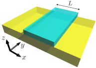
In this section, we investigate charge transport in a silicene pn junction, which is illustrated in Fig. 3.
III.1 Normal incident case
III.1.1 Formalism of the scattering problem
Firstly, we investigate a normal incident of a pn junction of silicene for . The Hamiltonian is given by
| (4) |
Hereafter, we focus only on the K point (). The same analysis is applicable to the K′ point.
We solve the scattering problem of the pn junction. The calculation has been done by employing theories for grapheneKatsnelson et al. (2006); Beenakker (2008); Cayssol et al. (2009) and the Kane-Mele model.Yamakage et al. (2009, 2011) In the incident side (), an external electric field is not applied and hence the energy bands are doubly degenerated. As a result, there are two incident states for a fixed incident energy . Wave function of the scattering state with the incident energy being has the form as
| (5) | ||||
| (6) |
where the subscript of denotes the spin state of the incident state . The first term of Eq. (5) denotes the incident state. The other two terms correspond to the reflected states with the same () and different (spin-flip, ) spin states. Momentum of the incident electron is given by
| (7) |
The sign of is determined so that the group velocity of the incident state is positive. Note that the incident state must be a propagating mode; . Otherwise, the corresponding conductance is zero, by definition. On the other hand, momentum of the transmitted electron is obtained by solving the following equation;
| (8) |
Since the group velocities of the transmitted electrons should be positive, the following relation is satisfied for the propagating mode;
| (9) |
For the evanescent mode, on the other hand, is satisfied. And note that when , the system in becomes insulating, i.e., the resulting conductance vanishes.
The reflection and transmission coefficients and are obtained by solving the continuity condition at . Since the charge current is conserved, the following relation holds.
| (10) |
where is the velocity operator. The above relation is reduced to
| (11) |
Solving this, one obtains the reflection and transmission coefficients. From the reflection coefficient , the transmission probability is given by
| (12) |
Charge conductance in the normal incident case () is defined by
| (13) |
III.1.2 Charge transport asymmetry in the nn and pn regimes
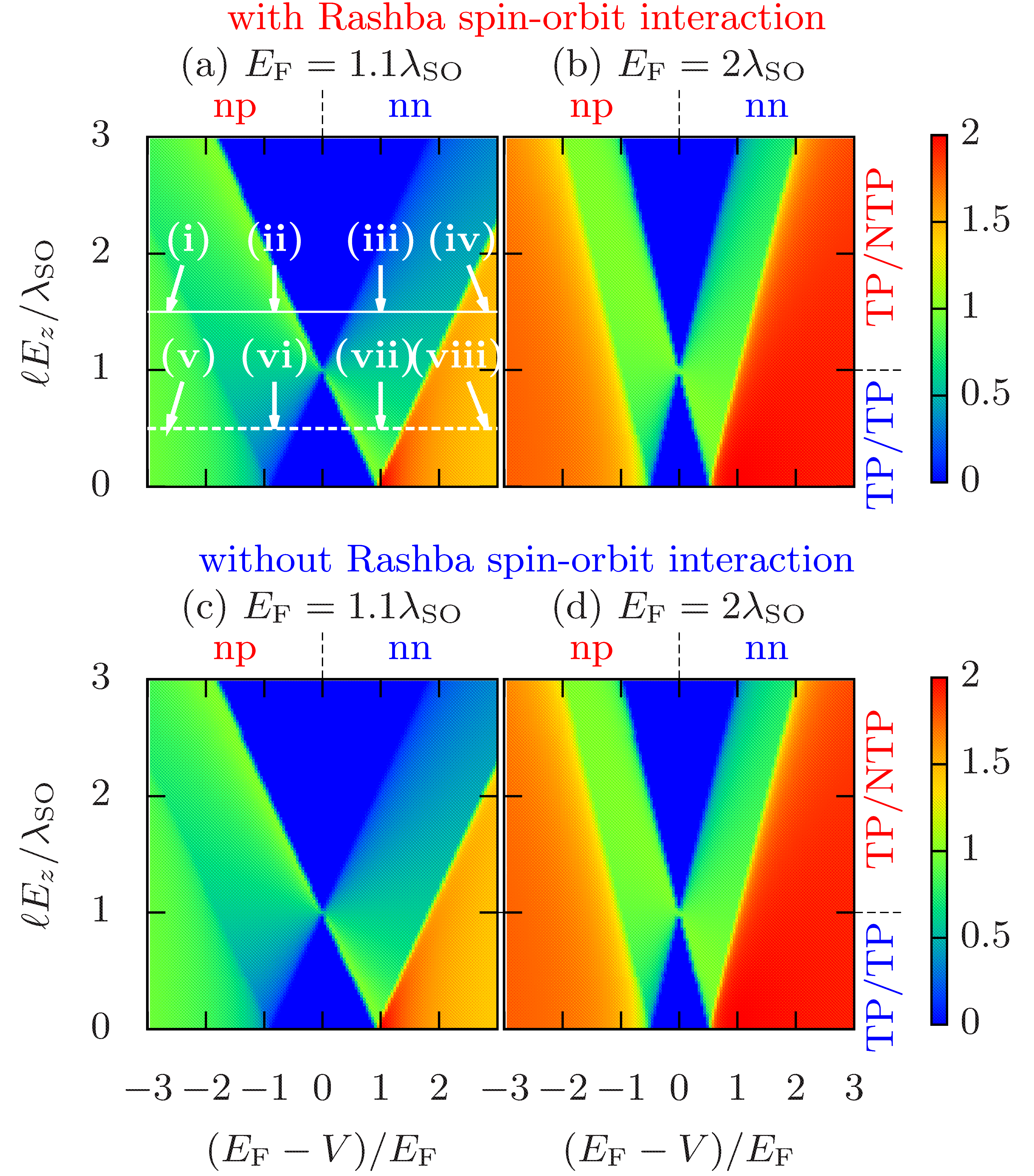
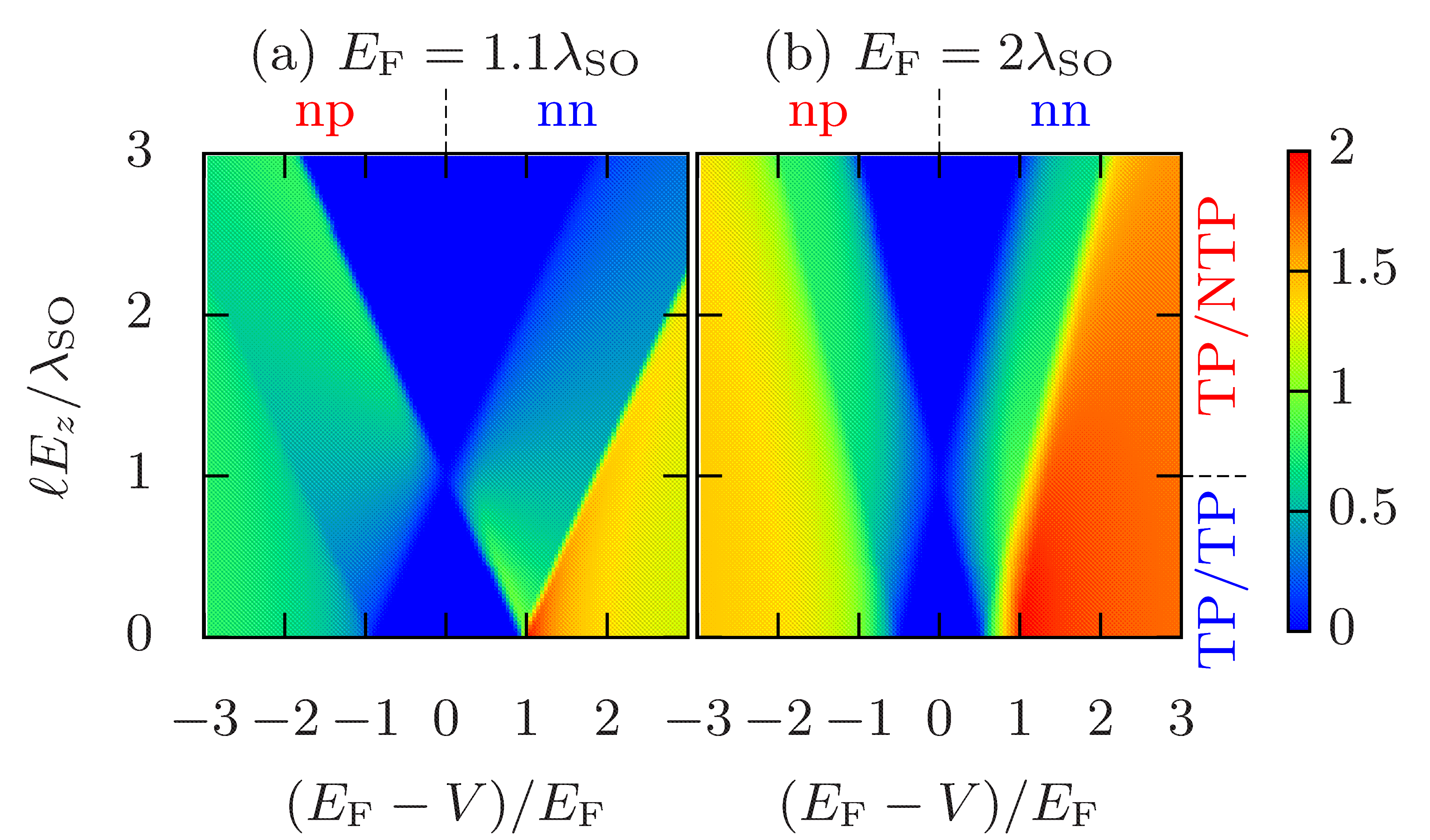
We show results on the conductance of the normal incident case () in Fig. 4. The horizontal axis is , where corresponds to the Fermi energy in measured from the charge neutrality point. The vertical axis is .
Note that and are not actually independent of each other since both of them are induced by the gate electric field. Therefore, the conductance along a curve in the plane of Fig. 4 is realized in the actual pn junction. The relation between and depend on the substrate. It is worthwhile to investigate the general conductance formula depending on and .
Only the region of is shown since the transmission probability is symmetric with respect to (See Appendix B). A pn junction with two doped topological insulators (TP/TP) is realized for . On the other hand, that with doped topological and non-topological (TP/NTP) insulators is realized for . Clearly seen from Fig. 4, there is no qualitative difference between the conductances with [Figs. 4(a) and (b)] and without [Figs. 4(c) and (d)] the sublattice-dependent Rashba SOI . This is because for silicene () is weak and furthermore vanishes at the K and K′ points.
For , one can obtain a simple formula for the reflection coefficient. The reflection coefficient with being the -component of spin of the incident electron is given by
| (14) |
with
| (15) |
The conductance is given by . If and , the corresponding tends to zero, i.e., a perfect transmission occurs, which is known as the Klein tunneling in monolayer graphene.Katsnelson et al. (2006); Beenakker (2008)
Here we go back to Fig. 4. In the inner region of , the conductance vanishes since the transmitted side () is insulating. In the central region of , there is a single energy band at the Fermi level, hence the maximum value of resultant conductance is . On the other hand, in the outer region of , two energy bands are located at the Fermi level. Here the conductance becomes larger (almost double) than that in the central region. We refer to these regions as insulating, single-channel, and double-channel regimes, respectively. This behavior originates from a peculiarity of silicene, i.e., the band gap and spin-split energy bands owing to SOI and electric-field effect in the buckling structure. Graphene, in contrast, does not have SOI nor the buckling structure. The resulting conductance is always .
For the lightly doped case [, Figs. 4(a) and 4(c)], one can see asymmetry of the conductance with respect to . To be more explicit we show the conductance as a function of for (TP/NTP junction) and (TP/TP junction) in Fig. 5.
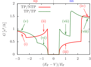
For the double-channel regime (), the transmission probabilities of the TP/NTP and TP/TP junctions are similar for both np [(i) and (v)] and nn [(iv) and (viii) case]. The transmission probability in the nn regime [(iv) and (viii)] is slightly larger than that in the np regime [(i) and (v)]. In contrast, for the single-channel regime () [(ii), (iii), (vi), and (vii)], the conductances of the TP/NTP and TP/TP junctions are qualitatively different. Namely, the conductance for the TP/NTP (TP/TP) junction in the np (nn) regime (ii) [(vii)] takes a larger value than that in the nn (np) regime (iii) [(vi)]. Note that the gate-voltage dependence of the conductance for the TP/NTP junction is distinct to that for the TP/TP junction.
This asymmetric behavior of conductance stems from the sublattice and spin states of the incident and transmitted electrons.
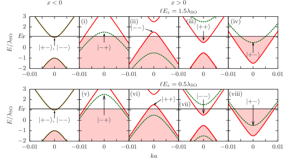
Figure 6 shows the energy bands for and . The sublattice and spin states for each energy band at are also denoted in Fig. 6. The incident states () with a positive energy are approximately given by and . When the transmitted states is given by [(ii) and (vii)] or [(iv) and (viii)], the conductance is large, due to matching of the sublattice and spin states. Especially, for and , the transmission probabilities are unity since the sublattice and spin states of the incident and transmitted electrons coincide with each other. In contrast, when the transmitted state is given by the mismatched state [(iii) and (vi)] or [(i) and (v)], the corresponding conductance is suppressed. Thus the matching/mismatching of the sublattice and spin states gives a larger/smaller conductance.
It is emphasized that the transmitted states and are controlled by . As shown in Fig. 1, the two states and are interchanged in the different topological phases, which is determined by . In other words, the conductance is well tuned by through changing the symmetry of the wave function. The obtained results are summarized in Table. 1. The same behavior has been observed in Ref. Yokoyama et al., 2010 on the surface of a topological insulator with ferromagnets.
| np | nn | |
|---|---|---|
| TP/NTP | large | small |
| TP/TP | small | large |
As explained above, the conductance controlled by is determined by the matching of the sublattice and spin states between the both sides of the junction. Therefore, this behavior does not appear in the heavily doped case () [Figs. 4(b) and 4(d)], where the mass gap is negligible as compared to . The conductance asymmetry peculiar to the topological phase can be expected for other topological insulators, provided that the system has a single Fermi surface in the pn junction.
III.1.3 Heavily doped case
From Figs. 4 (b) and (d), the transmission probability is almost quantized to be 0 for the insulating case (), to 1 for the single-channel regime (), and to 2 for the double-channel regime (). This is a consequence of the Klein tunneling of Dirac fermions: A massless Dirac fermion can tunnel through any barriers. Hence the normal incident transmission probability is unity.Katsnelson et al. (2006); Beenakker (2008) Although silicene has a finite energy gap, a perfect transmission approximately occurs for a heavily doped case, since the energy gap is effectively ignored as compared to the incident energy. In contrast, a graphene pn junction always shows a perfect transmission, i.e., the value of conductance is always . Thus graphene cannot be used as a FET.
III.2 Obliquely incident case
Next we turn to the case of finite , which corresponds to an actual silicene pn junction. The Hamiltonian of the two-dimensional system in the vicinity of the K point reads
| (16) |
Here we assume translational invariance along the -axis, i.e., the -component of momentum is regarded as a parameter. We solve the scattering problem in the same way as in the previous section.
The normalized conductance is given by
| (17) |
with being the transmission probability for an incident angle defined by and for incident spin . In the case of perfect transmission (), the resulting conductance takes the value of , where factor 2 means that the system has two incident states and with different spin states. Here, , , and being the width of the system. Also, Fano factor , which corresponds to the shot noise-to-signal ratio, is given by
| (18) |
Figure 7 shows the normalized charge conductance as a function of gate voltage [] and electric field ().
Obviously, the charge conductance (Fig. 7) and the transmission probability of the normal incident case [Figs. 4(a) and 4(b)] are almost the same, except for the broadening of line shape. This is because transport is determined basically by the normal incidence. An integral over the incident angle solely gives line broadening of the charge conductance from that for the normal incidence .
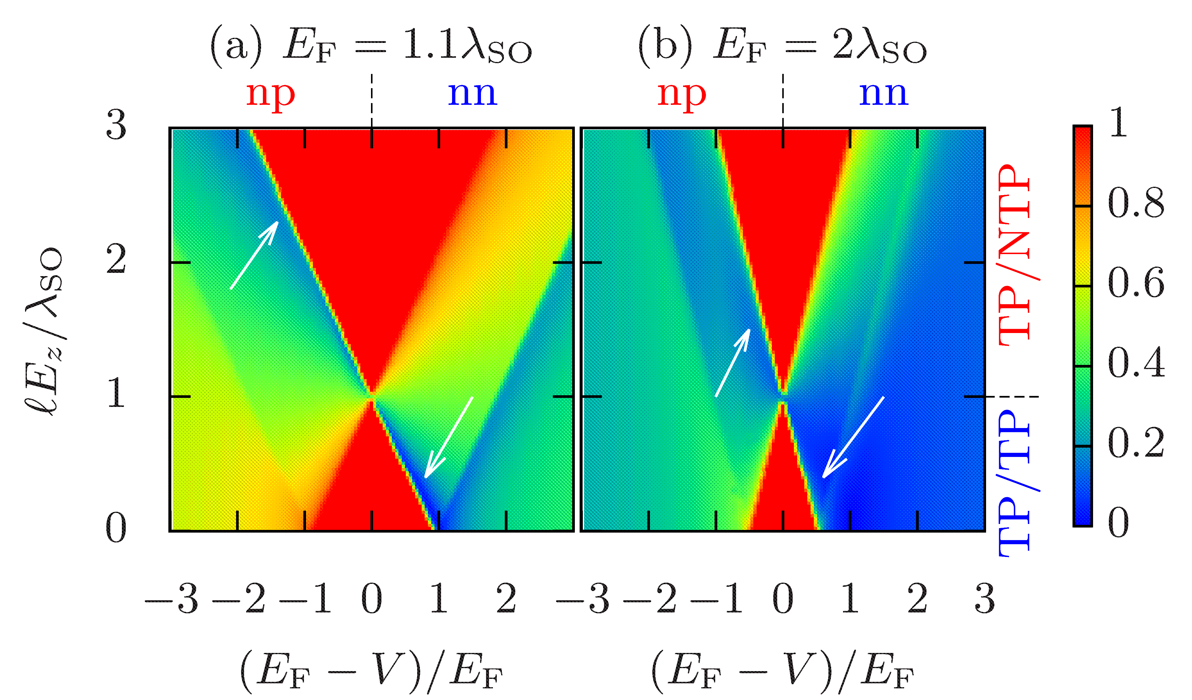
The Fano factor of the junction is shown in Fig. 8. Overall, the resulting Fano factor for the lightly doped case (a) is smaller than that for the heavily doped case (b). Also, the Fano factor is roughly given by the inverse of conductance, i.e., it takes a small (large) value when the corresponding conductance is large (small). This behavior is realized if the shot noise power is almost independent of the parameters ( and ). On the other hand, in the single-channel regime, the Fano factor is strongly suppressed when the sublattice and spin states of the incident and transmitted electrons coincide with each other (denoted by the arrows in Fig. 8). Note that the Fano factor in the insulating region () is obtained to be unity, although it is not well-defined for metal-insulator junctions because the corresponding conductance vanishes (). We have concluded in the insulating region since has been obtained for the long junction limit of the npn junction, as discussed in the next section.
IV silicene npn junction
Next we investigate charge transport in a silicene npn junction, where electrostatic field is applied in , which is illustrated in Fig. 9.
The scattering problem of the npn junction is solved in a manner similar to that of the pn junction. The wave function is given by
| (19) | ||||
| (20) | ||||
| (21) |
where and are solutions of . Coefficients , , and are obtained by solving the following boundary condition:
| (22) | ||||
| (23) |
The normalized conductance and the Fano factor are obtained by Eqs. (17) and (18), respectively.
IV.1 Normal incident case
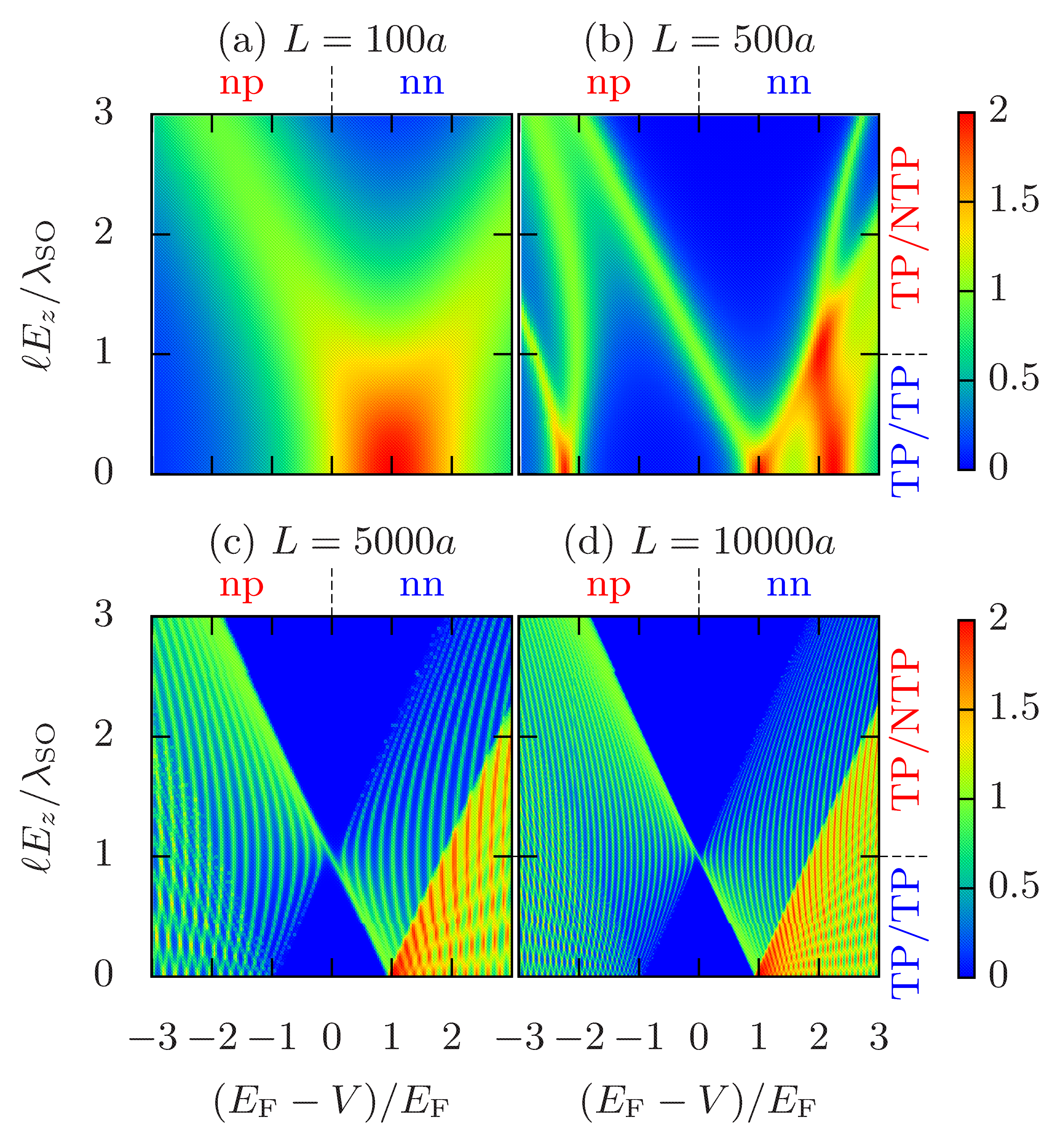
First we show the conductance for the normal incident case in Fig. 10, i.e., . A resonant tunneling occurs for in a npn junction. In the short junction limit (), a perfect transmission always occurs even when the central region is insulating. In a short but finite-length junction [Fig. 10(a)], the number of resonant peaks () is still small (two peaks). On the other hand, the peak width is broad () since the length of the junction is short so that the transmission probability is large. Thus, two broad resonant peaks appear in Fig. 10(a). As one increases , the number of resonant peaks increases and the peak width becomes narrower, as shown in Figs. 10(b) and 10(c). Finally, the transmission probability of the long junction () [Fig. 10(d)] asymptotically converges to that of the pn junction [Fig. 4(a)].
IV.2 Obliquely incident case
Next we show results on the obliquely incident case.
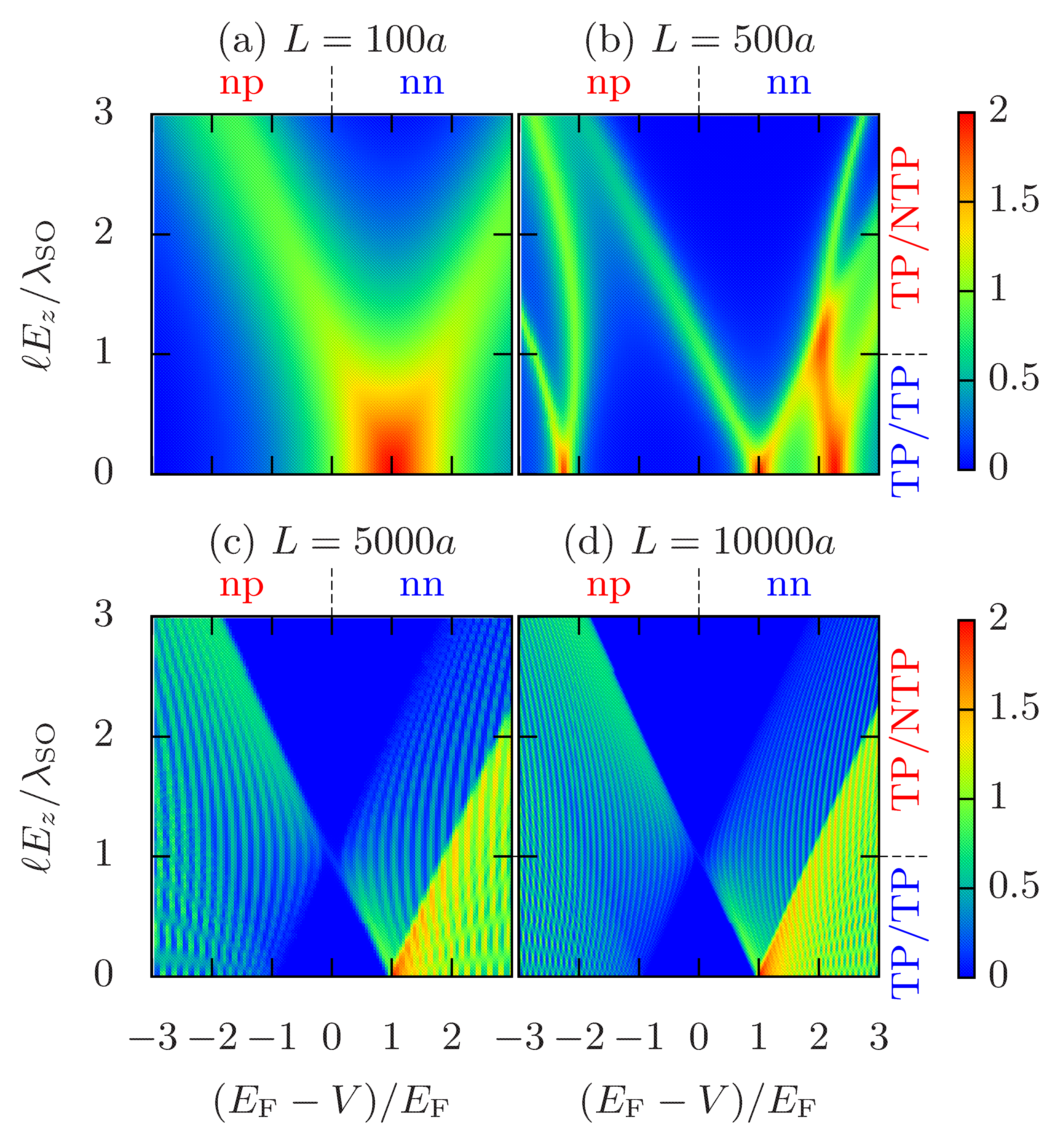
The charge conductance is shown in Fig. 11. As in the case of the pn junction discussed in Sec. III.2, integral over the incident angle entirely causes broadening of detail structures in the conductance. Namely, the conductance [Figs. 11(a)-(d)] is almost the same as that of the normal incident case [Figs. 10(a)-(d)].
In addition, we show the Fano factor in Fig. 12.
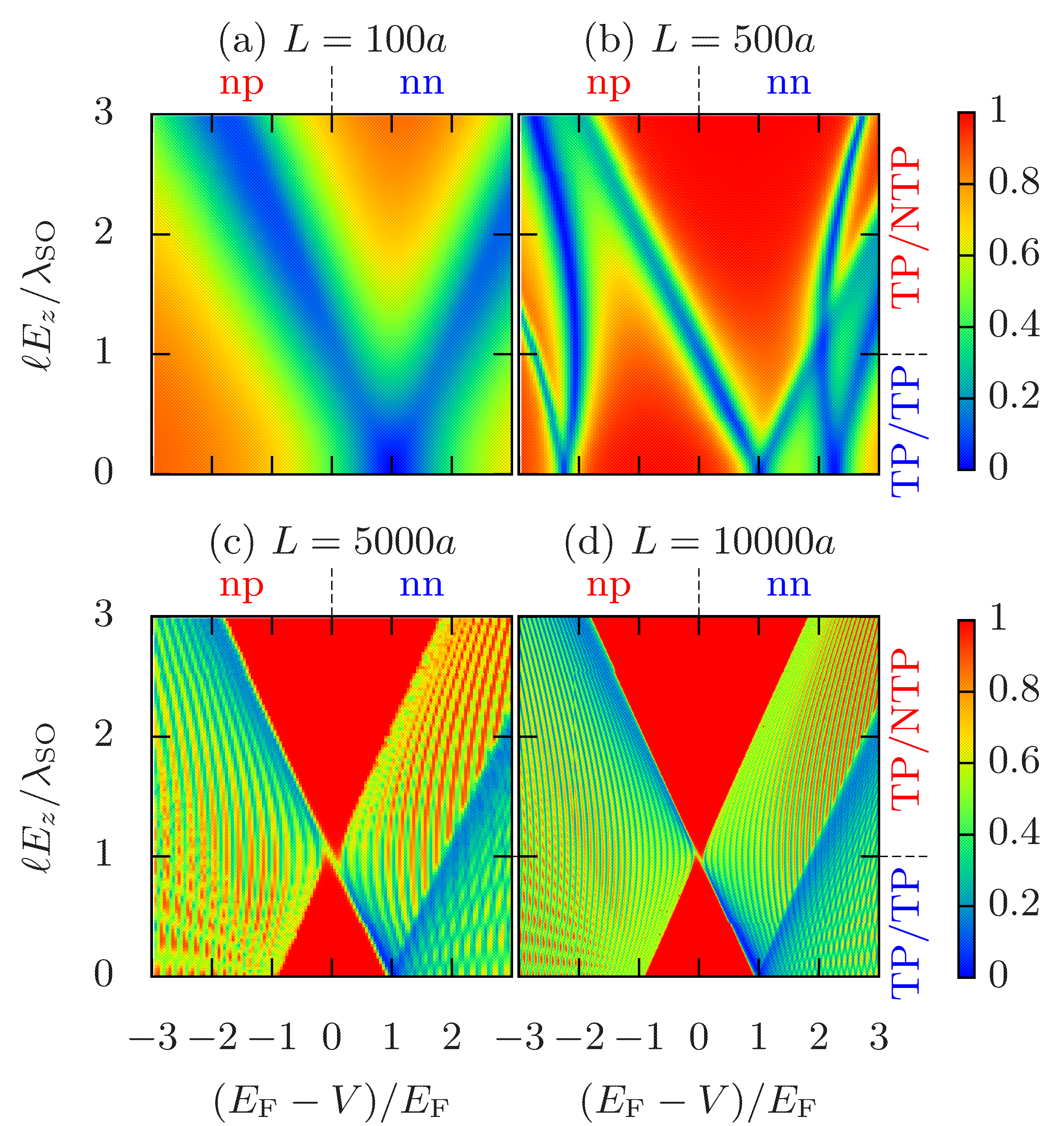
The Fano factor (Fig. 12) is basically given by the inverse of (Fig. 11): takes a small value for a resonant tunneling case. In the long junction limit [Figs. 12(c) and 12(d)], of the npn junction tends to that of the pn junction [Fig. 8(a)]. And also, in the insulating regime , converges to be unity. Namely, the Fano factor is interpreted to be unity for the insulating regime of pn junction.
V Summary
We have studied charge transport in the pn and npn junctions of silicene. In silicene, the topological phase transition occurs by applying electric field owing to the buckling structure. This transition affects the charge transport for the single-channel regime, i.e., the resulting conductance is suppressed in the np regime for the TP/TP junction, while it is suppressed in the nn regime for the TP/NTP junction. We have shown that this suppression originates from matching/mismatching of the spin and sublattice states of the incident and transmitted electrons. Furthermore, the silicene pn junction has been shown to be a FET which conductance is almost quantized. It is not the case in the graphene pn junction, which has no band gap. The silicene junctions can be a potential new device controlled by two types of electric field and .
Acknowledgements.
This work is supported by the “Topological Quantum Phenomena” (No. 22103005) Grant-in Aid for Scientific Research on Innovative Areas from the Ministry of Education, Culture, Sports, Science and Technology (MEXT) of Japan. MH is supported by Grant-in Aid for Scientific Research No. 22740196.Appendix A Wave function in bulk silicene
The low-energy Hamiltonian Eq. (1) is rewritten as
| (24) |
with . We diagonalize this Hamiltonian sequentially, i.e., diagonalizing the spin part () in the first step and sublattice pseudo spin () in the next step. The eigenvalue of is obtained to be with
| (25) |
The corresponding eigenvector is given by
| (26) |
As a result, the partially diagonalized Hamiltonian is given by
| (27) |
Thus, the energy spectrum is obtained to be with
| (28) |
The corresponding eigenvector is given by the direct product of the eigenvectors of the pseudo spin and the spin as
| (29) |
with
| (30) |
Appendix B Symmetry
In this Appendix, we show the symmetry of the conductance in the silicene junction. Applying -rotation along the -axis, one obtains
| (31) |
The eigenvector is transformed as
| (32) |
These lead to
| (33) |
It follows that the charge conductance, which is obtained by the integral over , , and , is an even function of .
Next, we show the relation of the conductance between the two valleys. Applying unitary transformation , the Hamiltonian is transformed as
| (34) |
The eigenvector is also transformed as
| (35) |
From Eqs. (33) and (35), we conclude that the conductances contributed from K and K′ points are equivalent to each other.
References
- Novoselov et al. (2004) K. S. Novoselov, A. K. Geim, S. V. Morozov, D. Jiang, Y. Zhang, S. V. Dubonos, I. V. Grigorieva, and A. A. Firsov, Science 306, 666 (2004).
- Vogt et al. (2012) P. Vogt, P. De Padova, C. Quaresima, J. Avila, E. Frantzeskakis, M. C. Asensio, A. Resta, B. Ealet, and G. Le Lay, Phys. Rev. Lett. 108, 155501 (2012).
- Fleurence et al. (2012) A. Fleurence, R. Friedlein, T. Ozaki, H. Kawai, Y. Wang, and Y. Yamada-Takamura, Phys. Rev. Lett. 108, 245501 (2012).
- Lin et al. (2012) C.-L. Lin, R. Arafune, K. Kawahara, N. Tsukahara, E. Minamitani, Y. Kim, N. Takagi, and M. Kawai, Appl. Phys. Express 5, 045802 (2012).
- Kane and Mele (2005a) C. L. Kane and E. J. Mele, Phys. Rev. Lett. 95, 226801 (2005a).
- Kane and Mele (2005b) C. L. Kane and E. J. Mele, Phys. Rev. Lett. 95, 146802 (2005b).
- Min et al. (2006) H. Min, J. E. Hill, N. A. Sinitsyn, B. R. Sahu, L. Kleinman, and A. H. MacDonald, Phys. Rev. B 74, 165310 (2006).
- Yao et al. (2007) Y. Yao, F. Ye, X.-L. Qi, S.-C. Zhang, and Z. Fang, Phys. Rev. B 75, 041401 (2007).
- Liu et al. (2011a) C.-C. Liu, W. Feng, and Y. Yao, Phys. Rev. Lett. 107, 076802 (2011a).
- Klein (1929) O. Klein, Z. Phys. 53, 157 (1929).
- Katsnelson et al. (2006) M. I. Katsnelson, K. S. Novoselov, and A. K. Geim, Nat. Phys. 2, 620 (2006).
- Beenakker (2008) C. W. J. Beenakker, Rev. Mod. Phys. 80, 1337 (2008).
- Ando et al. (1998) T. Ando, T. Nakanishi, and R. Saito, J. Phys. Soc. Jpn. 67, 2857 (1998).
- Huard et al. (2007) B. Huard, J. A. Sulpizio, N. Stander, K. Todd, B. Yang, and D. Goldhaber-Gordon, Phys. Rev. Lett. 98, 236803 (2007).
- Shytov et al. (2008) A. V. Shytov, M. S. Rudner, and L. S. Levitov, Phys. Rev. Lett. 101, 156804 (2008).
- Young and Kim (2009) A. F. Young and P. Kim, Nat. Phys. 5, 222 (2009).
- Saito et al. (2007) K. Saito, J. Nakamura, and A. Natori, Phys. Rev. B 76, 115409 (2007).
- Sonin (2009) E. B. Sonin, Phys. Rev. B 79, 195438 (2009).
- Yokoyama et al. (2009) T. Yokoyama, Y. Tanaka, and N. Nagaosa, Phys. Rev. Lett. 102, 166801 (2009).
- Bercioux and De Martino (2010) D. Bercioux and A. De Martino, Phys. Rev. B 81, 165410 (2010).
- Bai et al. (2010) C. Bai, J. Wang, S. Jia, and Y. Yang, App. Phys. Lett. 96, 223102 (2010).
- Ingenhoven et al. (2010) P. Ingenhoven, J. Z. Bernád, U. Zülicke, and R. Egger, Phys. Rev. B 81, 035421 (2010).
- Rataj and Barnaś (2011) M. Rataj and J. Barnaś, App. Phys. Lett. 99, 162107 (2011).
- Bai et al. (2011a) C. Bai, J. Wang, Y. Zhang, and Y. Yang, App. Phys. A 103, 427 (2011a).
- Bai et al. (2011b) C. Bai, J. Wang, S. Jia, and Y. Yang, Physica E 43, 884 (2011b).
- Niu (2011) Z. P. Niu, J. Phys.: Cond. Matt. 23, 435302 (2011).
- Guigou et al. (2011) M. Guigou, P. Recher, J. Cayssol, and B. Trauzettel, Phys. Rev. B 84, 094534 (2011).
- Liu et al. (2012) M.-H. Liu, J. Bundesmann, and K. Richter, Phys. Rev. B 85, 085406 (2012).
- Esmaeilzadeh and Ahmadi (2012) M. Esmaeilzadeh and S. Ahmadi, J. App. Phys. 112, 104319 (2012).
- Tian et al. (2012a) H. Y. Tian, K. S. Chan, and J. Wang, Phys. Rev. B 86, 245413 (2012a).
- Tian et al. (2012b) H. Y. Tian, Y. H. Yang, and J. Wang, Eur. Phys. J. B 85, 1 (2012b).
- Rothe et al. (2012) D. G. Rothe, E. M. Hankiewicz, B. Trauzettel, and M. Guigou, Phys. Rev. B 86, 165434 (2012).
- Prada and Metalidis (2013) E. Prada and G. Metalidis, J. Comp. Elec. 12, 63 (2013).
- Ezawa (2012a) M. Ezawa, New J. Phys. 14, 033003 (2012a).
- Takeda and Shiraishi (1994) K. Takeda and K. Shiraishi, Phys. Rev. B 50, 14916 (1994).
- Ohta et al. (2006) T. Ohta, A. Bostwick, T. Seyller, K. Horn, and E. Rotenberg, Science 313, 951 (2006).
- McCann and Fal’ko (2006) E. McCann and V. I. Fal’ko, Phys. Rev. Lett. 96, 086805 (2006).
- McCann (2006) E. McCann, Phys. Rev. B 74, 161403 (2006).
- Oostinga et al. (2008) J. B. Oostinga, H. B. Heersche, X. Liu, A. F. Morpurgo, and L. M. K. Vandersypen, Nat. Mater. 7, 151 (2008).
- Zhang et al. (2009) Y. Zhang, T.-T. Tang, C. Girit, Z. Hao, M. C. Martin, A. Zettl, M. F. Crommie, Y. R. Shen, and F. Wang, Nature (London) 459, 820 (2009).
- Ezawa (2012b) M. Ezawa, Phys. Rev. Lett. 109, 055502 (2012b).
- Ezawa (2013a) M. Ezawa, Phys. Rev. Lett. 110, 026603 (2013a).
- Ezawa (2013b) M. Ezawa, Phys. Rev. B 87, 155415 (2013b).
- Ezawa (2013c) M. Ezawa, Appl. Phys. Lett. 102, 172103 (2013c).
- Tsai et al. (2013) W.-F. Tsai, C.-Y. Huang, T.-R. Chang, H. Lin, H.-T. Jeng, and A. Bansil, Nat. Commun. 4, 1500 (2013).
- Liu et al. (2011b) C.-C. Liu, H. Jiang, and Y. Yao, Phys. Rev. B 84, 195430 (2011b).
- Cayssol et al. (2009) J. Cayssol, B. Huard, and D. Goldhaber-Gordon, Phys. Rev. B 79, 075428 (2009).
- Yamakage et al. (2009) A. Yamakage, K.-I. Imura, J. Cayssol, and Y. Kuramoto, Europhys. Lett. 87, 47005 (2009).
- Yamakage et al. (2011) A. Yamakage, K.-I. Imura, J. Cayssol, and Y. Kuramoto, Phys. Rev. B 83, 125401 (2011).
- Yokoyama et al. (2010) T. Yokoyama, Y. Tanaka, and N. Nagaosa, Phys. Rev. B 81, 121401 (2010).