Current-driven domain wall motion with spin Hall effect: Reduction of threshold current density
Abstract
We theoretically study the current-driven domain wall motion in the presence of both the spin Hall effect and an extrinsic pinning potential. The spin Hall effect mainly affects the damping ratio of the domain wall precession in the pinning potential. When the pinning potential is not too strong, this results in a significant reduction of a threshold current density for the depinning of a domain wall with certain polarity. We also propose one way to distinguish the spin Hall effect induced spin-transfer torque from the one induced by the Rashba spin-orbit coupling experimentally.
An electric control of magnetization by the spin-transfer torque (STT) berger1996 ; slonczewski1996 is under intense investigation due to its device application potentials. parkin2008 ; allwood2005 An essential prerequisite for the STT is to generate a spin flow of electrons. A simple intuitive method is to utilize spin-polarized conduction electrons in a ferromagnetic layer (FM). parkin2008 ; allwood2005 ; yamanouchi2004 ; klaui2005 ; yamaguchi2004 Recently, a very different way to generate a spin flow was proposed, liu2011 ; liu2012prl ; liu2012science ; haazen2012 which utilizes a pure spin current generated by the spin Hall effect (SHE). hirsch1999 ; zhang2000 When a charge current flows in a nonmagnetic layer (NM) with strong atomic spin-orbit coupling, the SHE generates a pure spin current in the direction perpendicular to the charge current. Thus, when a thin FM is deposited on the NM, the pure transverse spin current is injected to the FM and generates the STT. Recent experiments liu2012prl ; liu2012science ; haazen2012 demonstrated that the STT generated by the spin current can be strong enough to switch the magnetization direction of the FM. The magnitude of the spin current is often parameterized by the spin Hall angle, denoting the ratio between the source charge current density and the resulting spin current density. The spin Hall angle was estimated to be for Pt liu2012prl and for -Ta. liu2012science Here, the opposite signs of the Pt and -Ta spin Hall angles imply opposite spin direction of the spin current in the two cases.
The SHE-induced STT (SHE-STT) can modify the current-driven domain wall (DW) motion. An in-plane electric current in a FM/NM system can generate the DW motion through two mechanisms. In one mechanism, the spin-polarized charge current flowing in the FM generates adiabatic and nonadiabatic STTs, tatara2004 ; zhang2004 ; thiaville2005 of which effect on the DW motion has been examined extensively. The other mechanism is the pure spin current injected from the NM due to the SHE. A recent theoretical study smseo2012 examined the effect of the SHE-STT on the current-driven DW motion in an ideal situation without any pinning centers suppressing the DW motion. Such an ideal condition is rarely achieved in practical situations, however, and it is well known tatara2006 ; jryu2009 that pinning centers may affect the DW motion considerably. Also from an application point of view, pinning centers are needed to achieve reliable control of DW locations in DW-based devices. Notches klaui2005 or local modulation of magnetic properties yamanouchi2004 are commonly suggested forms of pinning centers for device applications. In this Letter, we study the SHE-STT effects on the current-driven DW motion in the presence of an extrinsic pinning potential. We show that the SHE can significantly reduce the threshold current density to depin a DW from the pinning potential, thereby lowering the energy cost for the operation of DW-based devices.
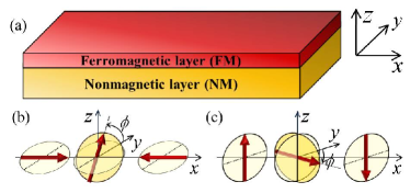
We consider a bi-layered system consisting of a thin FM deposited on a NM [Fig. 1(a)]. The current-driven DW motion in this system can be described by generalizing the standard Landau-Lifshitz-Gilbert (LLG) equation smseo2012 ; liu2011 to include the SHE-STT. In this study, we use the collective coordinate approach, thiele1973 ; swjung2008 in which DW dynamics is described by two collective coordinates, DW position (along -direction) and tilting angle [see Figs. 1(b) and (c) for its definition in in-plane magnetic anisotropy (IMA) system and perpendicular magnetic anisotropy (PMA) system, respectively]. Although this approach has some limitations especially for vortex DWs, it was found to be a very useful tool smseo2012 to analyze transverse DWs that we consider [Figs. 1(b) and (c)]. Interestingly, for both IMA [Fig. 1(b)] and PMA [Fig. 1(c)] systems, this approach results in the identical equations of motion describing the coupled dynamics of and , swjung2008 ; smseo2012 ; tatara2006
| (1) | ||||
where is the Gilbert damping constant, is the DW width, is the gyromagnetic ratio, is the hard-axis anisotropy field, is the magnitude of the adiabatic STT in the velocity dimension, is the magnitude of the nonadiabatic STT, is the saturation magnetization, is an extrinsic pinning potential, and represents the magnitude of the SHE-STT. Here, and are the thickness and spin polarization of the FM, is the spin Hall angle of the system, and is the current density in the NM(FM). is assumed to be a finite-ranged harmonic potential placed at : where is the unit step function centered at . Here, and are the depth and range of the pinning potential. For analysis, it is convenient to rewrite Eq. (1) in terms of dimensionless quantities as
| (2) | ||||
Here, , , , and .
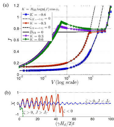
To investigate the SHE-STT effects in the presence of , we first calculate the threshold current density , above which a DW can get depinned from the pinning potential. In our simulation, a DW is placed at the center of the pinning potential () with the initial tilting angle (or polarity) or . The current pulse is then turned on with zero rising time. Figure 2(a) shows the numerical simulation result obtained with , and . These parameter choices may be applicable to an IMA bi-layer system such as Pt/Py. liu2011 In the absence of the SHE [black solid line in Fig. 2(a)], it is well known tatara2006 that depends on in three distinct ways. In the so-called intermediate regime [ in Fig. 2(a)], the adiabatic STT tatara2006 ; swjung2008 ; koyama2011 is the main depinning mechanism and is almost independent of , with value similar to the intrinsic threshold value. tatara2004 For smaller (weak pinning regime, ) and larger (strong pinning regime, ) , the nonadiabatic and adiabatic STTs are respectively the main depinning mechanisms overcoming the extrinsic pinning potential and increases as increases. A thick (nm) Py layer klaui2005 ; parkin2008 ; yamaguchi2004 can have small in the weak pinning regime. But when a Py layer is made thin ( a few nm liu2011 ), which increases the SHE-STT since is inversely proportional to , is expected to be larger due to the enhanced interface contribution to . Thus a SHE bi-layer system is likely to be near the borderline between the weak and intermediate pinning regimes. Interestingly, it turns out that this is the range where the SHE-STT effects are most pronounced. Numerical simulation of Eq. (2) indicates a significant reduction of in this range if [ and for red circular and blue squared symbols in Fig. 2(a)]. On the other hand, changes only mildly in this range if [ and for purple diamond and green triangular symbols in Fig. 2(a)]. Note that for a given sign of (or ), the SHE reduces significantly only for a DW with a proper sign of (or proper DW polarity). Hence, one can control the depinning efficiency by preparing the initial DW polarity to a proper value.
We remark that for metallic ferromagnets with IMA liu2011 , our estimation of . Here, we assume , , , , and .
To understand the origin of the reduction, we further analyze dynamics. Within the pinning range [], two equations in Eq. (2) can be combined into the following nd order partial differential equation for dynamics,
| (3) | ||||
For small , stays near its initial value , which is either or . Thus, to get an insight, we expand above equation near to obtain
| (4) |
where
| (5) |
Here, and are an undamped angular frequency and the damping ratio, respectively. For , is always positive and approaches towards its stable steady value. The accompanied dynamics is shown in Fig. 2(b) as blue dash-dotted () and green dashed () lines. In the presence of the SHE (), however, is not necessarily positive and may become negative if is negative and sufficiently large in magnitude. When , dynamics does not have a stable steady value and results in the DW depinning driven by the amplification of [and also as shown in Fig. 2(b), red solid line]. Thus the condition sets an upper bound on , that is, with
| (6) |
which is shown as black dashed and dash-dotted lines in Fig. 2(a) for and , respectively. In the region where the SHE reduces , note that is in good agreement with numerically calculated values [red circles and blue squares in Fig. 2(a)]. This demonstrates that the reduction of by the SHE arises because the SHE can induce negative and thus amplify the dynamics. For , on the other hand, the SHE increases and thus as well [purple diamond and green triangular symbols in Fig. 2(a)]. A slight decrease of in the weak pinning regime is due to the shift of the stable DW position. Note that one sign of reduces while the other increases it. Thus, to reduce , the DW polarity should be properly adjusted before the current injection, for example by applying weak in-plane magnetic field or injecting a properly designed train of small current pulses. thomas2006
Similar reduction of occurs in a PMA bi-layer as well, which is natural since IMA and PMA bi-layer systems share the same equations of motion for the DW depinning dynamics [Eq. (1)]. In particular, the upper bound in Eq. (6) applies equally to the PMA bi-layer. Thus the difference between the PMA and IMA bi-layers may come only through different material parameters. For the PMA bi-layer system -Ta/CoFeB with low Gilbert damping liu2012science , is estimated to be similar to or even smaller than the corresponding value in Fig. 2(a) for the IMA bi-layer system. For the PMA bi-layer system Pt/CoFeB, the reported value of ranges from liu2012science to 0.5 miron2011 . Since is proportional to , the reduction of due to the SHE is expected to be much less significant for the PMA system with large .
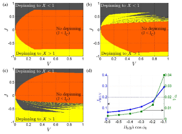
Next, we examine the depinning direction. In the absence of the SHE (), the DW gets depinned to the right (left) of the pinning center when electrons flow to the right (left) and thus the depinning direction agrees with the electron flow direction [Fig. 3(a)]. This direction remains the same even in the presence of the SHE if . On the other hand, when and , interestingly, the depinning direction is opposite to the electron flow direction in a wide range near [see upper yellow region in Fig. 3(b) and lower gray region in Fig. 3(c)].
This situation resembles the situation for the DW motion direction in an ideal wire without pinning centers. In the absence of the SHE, the terminal velocity of the DW is always along the electron flow direction. When the SHE exists, however, it was recently demonstrated smseo2012 that the terminal motion direction can be opposite to the electron flow direction if . Note that for both the depinning direction reversal and the terminal motion direction reversal, should be negative. Thus when the initial DW polarity satisfies this condition for a given sign of , the DW may get depinned against the electron flow direction and maintain the same motion direction. This raises a possibility that a DW may propagate against the electron flow direction without getting pinned in a nonideal nanowire containing pinning centers. This may also provide an explanation for the reversed DW motion observed experimentally, miron2011 without resorting to the Rashba spin-orbit coupling (RSOC) effect. kwkim2012 For this possibility to work, it is important to avoid the DW polarity switching or the sign change of , which sets a constraint; should be smaller than the certain current density value (), above which the DW polarity switching occurs. Thus, should fall in the current density window, . For such window to exist, the inequality should be satisfied. By numerical simulation, we calculate the threshold pinning potential depth , above which the inequality is violated. Firstly, for [blue circular symbols in Fig. 3(d)] is calculated. For , is of the order of which amounts to the current density of the order of for and . Then is compared with to extract [green squared symbols in Fig. 3(d)]. For , is smaller than which amounts to of the hard-axis anisotropy energy of a DW. swjung2008 Here, we used and where is the hard-axis anisotropy energy. To observe the DW motion against the electron flow direction, should be satisfied. Thus to explain the reversed DW motion in a recent experiment miron2011 with the SHE-STT (but without the RSOC effect kwkim2012 ), pinning centers should be very weak.
Lastly, recent theory kwkim2012 indicates that the RSOC-induced STT (RSOC-STT) may drive the DW against the electron flow direction in a FM sandwiched by two dissimilar layers such as metal and oxide. In this case, the so-calle field-like STT arising from the RSOC suppresses the DW polarity switching. Thus the DW motion against the electron flow direction can be maintained for relatively larger value of compared to the case with the SHE-only (without RSOC-STT) case. The strength of the extrinsic pinning potential can be controlled, for example by introducing the notch in the wire. Thus this feature may be used to distinguish the RSOC-STT and the SHE-STT in experiments.
In summary, we examine the SHE-STT effects on a DW motion in the presence of the extrinsic pinning potential. The presence of the SHE-STT mainly affects the damping ratio of a DW precession in the pinning potential and by inducing negative damping ratio, it can significantly reduce the threshold current density. We also examined the DW motion direction and found that the SHE-STT can induce a DW motion against the electron flow direction if the pinning potential is sufficiently weak. By using this dependence on the pinning potential strength, we suggest one way to distinguish the SHE-STT and RSOC-STT in the presence of the pinning potential.
References
- (1) J. C. Slonczewski, J. Magn. Magn. Mater. 159, L1 (1996).
- (2) L. Berger, Phys. Rev. B 54, 9353 (1996).
- (3) D. A. Allwood, G. Xiong, C. C. Faulkner, D. Atkinson, D. Petit, R. P. Cowburn, Science 309, 1688 (2005).
- (4) S. S. P. Parkin, M. Hayashi, and L. Thomas, Science 320, 190 (2008).
- (5) M. Kläui, C. A. F. Vaz, J. A. C. Bland, W. Wernsdorfer, G. Faini, E. Cambril, L. J. Heyderman, F. Nolting, and U. Rüdiger, Phys. Rev. Lett. 94, 106601 (2005).
- (6) M. Yamanouchi, D. Chiba, F. Matsukura, and H. Ohno, Nature 428, 539 (2004).
- (7) A. Yamaguchi, T. Ono, S. Nasu, K. Miyake, K. Mibu, and T. Shinjo Phys. Rev. Lett. 92, 077205 (2004).
- (8) T. Koyama, D. Chiba, K. Ueda, K. Kondou, H. Tanigawa, S. Fukami, T. Suzuki, N. Ohshima, N. Ishiwata, Y. Nakatani et al., Nat. Mat. 10, 194 (2011).
- (9) L. Liu, T. Moriyama, D. C. Ralph, and R. A. Buhrman, Phys. Rev. Lett. 106, 036601 (2011).
- (10) L. Liu, O. J. Lee, T. J. Gudmundsen, D. C. Ralph, and R. A. Buhrman, Phys. Rev. Lett. 109, 096602 (2012).
- (11) L. Liu, C.-F. Pai, Y. Li, H. W. Tseng, D. C. Ralph, and R. A. Buhrman, Science 336, 555 (2012).
- (12) P. P. J. Haazen, E. Muré, J. H. Franken, R. Lavrijsen, H. J. M. Swagten, and B. Koopmans, arXiv:1209.2320 (2012).
- (13) J. E. Hirsch, Phys. Rev. Lett. 83, 1834 (1999).
- (14) S. Zhang, Phys. Rev. Lett. 85, 393 (2000).
- (15) G. Tatara and H. Kohno, Phys. Rev. Lett. 92, 086601 (2004).
- (16) S. Zhang and Z. Li, Phys. Rev. Lett. 93, 127204 (2004).
- (17) A. Thiaville, Y. Nakatani, J. Miltat, and Y. Suzuki, Europhys. Lett. 69,990 (2005).
- (18) S.-M. Seo, K.-W. Kim, J. Ryu, H.-W. Lee, and K.-J. Lee, Appl. Phys. Lett. 101, 022405 (2012).
- (19) G. Tatara, T. Takayama, H. Kohno, J. Shibata, Y. Nakatani, and H. Fukuyama, J. Phys. Soc. Jpn. 75, 064708 (2006).
- (20) J. Ryu and H.-W. Lee, J. Appl. Phys. 105, 093929 (2009).
- (21) A. A. Thiele, Phys. Rev. Lett. 30, 230 (1973).
- (22) S.-W. Jung, W. Kim, T.-D. Lee, K.-J. Lee, and H.-W. Lee, Appl. Phys. Lett. 92, 202508 (2008).
- (23) I. M. Miron, P.-J. Zermatten, G. Gaudin, S. Auffret, B. Rodmacq, and A. Schuhl, Phys. Rev. Lett. 102, 137202 (2009).
- (24) Y. Tserkovnyak, H. J. Skadsem, A. Brataas, and G. E. W. Bauer, Phys. Rev. B 74, 144405 (2006)
- (25) I. M. Miron, T. Moore, H. Szambolics, L. D. Buda-Prejbeanu, S. Auffret, B. Rodmacq, S. Pizzini, J. Vogel, M. Bonfim, A. Xchuhl et al., Nat. Mat. 10, 419 (2011).
- (26) L. Thomas, M. Hayashi, X. Jiang, R. Moriya, C. Rettner, and S. S. P. Parkin, Nature 443, 197 (2006).
- (27) K.-W. Kim, S.-M. Seo, J. Ryu, K.-J. Lee, and H.-W. Lee, Phys. Rev. B 85, 180404(R) (2012).