Optical control of individual carbon nanotube light emitters by spectral double resonance in silicon microdisk resonators
Abstract
Single-walled carbon nanotubes have advantages as a nanoscale light source compatible with silicon photonics because they show room-temperature luminescence at telecom-wavelengths and can be directly synthesized on silicon substrates. Here we demonstrate integration of individual light-emitting carbon nanotubes with silicon microdisk resonators. Photons emitted from nanotubes are efficiently coupled to whispering gallery modes, circulating within the disks and lighting up their perimeters. Furthermore, we control such emission by tuning the excitation wavelength in and out of resonance with higher order modes in the same disk. Our results open up the possibilities of using nanotube emitters embedded in photonic circuits that are individually addressable through spectral double resonance.
pacs:
78.67.Ch, 42.82.Et, 78.55.-mAdvances in silicon photonics have enabled on-chip integration of various devices, Liang and Bowers (2010); Reed et al. (2010); Michel, Liu, and Kimerling (2010); Leuthold, Koos, and Freude (2010) expanding the capabilities of monolithic photonic circuits. For further scaling and increased functionality, however, integration of nanoscale emitters is desirable. Unfortunately, partly due to the fact that silicon is an indirect gap semiconductor, coupling of individually addressable nanoscale emitters to silicon photonics devices has remained a challenge.
In this regard, carbon nanotubes (CNTs) are promising because they are room-temperature telecom-band emitters O’Connell et al. (2002); Weisman and Bachilo (2003) that can be directly synthesized on silicon Kong et al. (1998) and be electrically driven.Misewich et al. (2003); Chen et al. (2005); Mann et al. (2007); Xia et al. (2008); Mueller et al. (2010) In particular, as-grown air-suspended CNTs show excellent optical properties,Lefebvre, Homma, and Finnie (2003); Chen et al. (2005); Mann et al. (2007) making them ideal for use as individual emitters compared to on-substrate Xia et al. (2008); Mueller et al. (2010) or solution based materials.Watahiki et al. (2012); Gaufrès et al. (2012)
As a silicon photonics device for coupling with air-suspended CNTs, microdisk resonators McCall et al. (1992) have many desirable properties. They are a commonly used microcavity structure, supporting whispering gallery modes (WGMs) where optical waves are guided along the circumference of the disk by continuous internal reflection. Because they can have ultra-high quality factors Borselli, Johnson, and Painter (2005); Soltani, Yegnanarayanan, and Adibi (2007) and small mode volumes, WGMs are suited for coupling with nanoscale emitters such as quantum dots.Michler et al. (2000); Peter et al. (2005); Mintairov et al. (2008) It is relatively easy to tune the cavity resonance to the emitter wavelength by fabricating disks with an appropriate diameter, and the three-dimensional structure of post-supported microdisks McCall et al. (1992); Michler et al. (2000); Peter et al. (2005) are compatible with air-suspended CNTs. Furthermore, they can be coupled to waveguides with high efficiency because they are traveling-wave resonators,Soltani, Yegnanarayanan, and Adibi (2007) making them a preferred choice compared to planar cavities Xia et al. (2008) for integration in silicon photonics.
Here we report on the integration of individual CNT emitters with silicon microdisks using fabrication processes compatible with standard silicon photonics. When photons emitted from nanotubes are coupled to the WGMs of the microdisks, emission enhancement occurs in a narrow spectral windows corresponding to the modes. Spatial imaging of the emission at the WGM wavelength shows the peripheral of the disk illuminated by the coupled CNT emission that circulates within the microdisk. In addition, we show that the excitation laser can also be coupled to whispering gallery modes in the same disk, allowing for non-local control over nanotube emission.
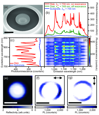
We fabricate microdisks from a silicon-on-insulator wafer with a 260-nm-thick top Si layer and a 2000-nm-thick buried oxide layer. Electron beam lithography and dry-etching processes are used to form doughnut-shaped trenches in the top Si layer. In order to create a post-supported disk structure, the buried oxide layer is etched in buffered hydrofluoric acid. A scanning electron microscope image of a typical microdisk prior to nanotube growth is shown in Fig. 1(a).
The devices are characterized with a home-built laser-scanning confocal photoluminescence (PL) microscopy system.Moritsubo et al. (2010); Yasukochi et al. (2011); Watahiki et al. (2012) An output of a wavelength-tunable continuous-wave Ti:sapphire laser is focused onto the sample by an objective lens to a spot size of 1 m. PL is coupled to a 300-mm spectrometer through a pinhole in a confocal configuration. An InGaAs photodiode array is used for detection and PL images are collected with a steering mirror. All measurements are done in air at room temperature.
A PL spectrum of a microdisk taken with an excitation wavelength nm and a power mW is shown as a red curve in Fig. 1(b). A forest of resonances consisting of WGMs as well as Fabry-Perot modes Mintairov et al. (2008) are visible within the silicon bandgap emission.
An interesting observation is that the emission intensity decreases by a factor of 5 when is tuned to 748 nm [green curve in Fig. 1(b)]. To investigate this strong excitation wavelength dependence, PL excitation (PLE) spectroscopy is performed [Fig. 1(c)-(d)]. We interpret the cross hatch pattern in the PLE map [Fig. 1(d)] as coupling of cavity modes at both excitation and emission wavelengths. The vertical streak-like features correspond to microdisk modes coupled to silicon emission, and the horizontal streaks represent modes coupled to the excitation laser. The intersections of vertical and horizontal streaks indicate simultaneous resonance of the excitation and emission, which allows control over PL intensity by about an order of magnitude [Fig. 1(b)].
The PLE spectrum [Fig. 1(c)] shows clear resonances with quality factors of 100, but precise mode assignment is difficult at these wavelengths because of high mode orders and strong absorption. Nevertheless, examination of reflectivity and PL images shows that PL is enhanced at the edges of the disk when the polarization matches the radial direction [Fig. 1(e)-(g)]. Such a polarization dependence is consistent with what one expects for WGMs with transverse-electric polarization. The coupling of excitation laser to WGMs implies that the laser photons can propagate within the disk at resonance, allowing for non-local excitation.
In order to couple single CNTs to microdisk WGMs, it is necessary to choose a disk with an appropriate diameter such that a suitable WGM exists at the emission wavelength of nanotubes. In addition, as CNTs interact primarily with light polarized along their axis,Hartschuh et al. (2003); Lefebvre et al. (2004); Moritsubo et al. (2010) it is also important to consider the mode polarization. WGMs can have either transverse-electric (TE) or transverse-magnetic (TM) polarization, and we expect TE modes to have better coupling with the nanotubes since CNTs suspended onto the microdisks will be parallel to the substrate.
We identify WGMs at CNT emission wavelengths by spin coating nanotube solution on the microdisks and performing PL measurements in a manner similar to experiments done on photonic crystal microcavities.Watahiki et al. (2012) Figure 2(a) shows spectra from a few microdisks with different diameters, and it can be seen that the mode wavelengths shift with diameter as expected.
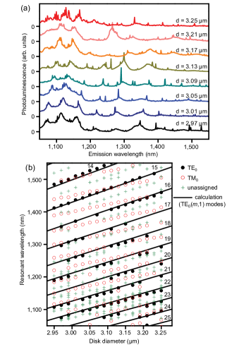
The disk diameter dependence of WGMs is summarized in Fig. 2(b). We assign the TE modes by comparing the data to an analytical model with no adjustable parameters.Borselli, Johnson, and Painter (2005) The TM modes are identified by a weaker dependence on the diameter, which is a result of their smaller effective index of refraction. Within the wavelength range of interest for coupling with CNTs (– nm), we confirm the presence of a few TE modes.
We now investigate CNT emitters integrated with silicon microdisks [Fig. 3(a)]. Another electron beam lithography step is performed to define catalyst windows at outer edges of the doughnut-shaped trenches. Single-walled CNTs are grown by chemical vapor deposition using ethanol as a carbon source.Maruyama et al. (2002) Catalyst solution is prepared by ultrasonicating 5.0 mg of cobalt(II) acetate tetrahydrate and 50.0 mg of fumed silica in 40.0 g of ethanol. We spin coat and lift off the catalyst solution, and the samples are annealed in air for 5 minutes at 400∘C prior to growth. The samples are then placed in a quartz tube furnace, and the temperature is elevated to 800∘C while flowing Ar with 3% H2. Ethanol is introduced by bubbling the carrier gas for 10 minutes. With some probability, nanotubes can get suspended across the trench onto the microdisk. By controlling the size of the catalyst areas, we are able to obtain a reasonable yield of 10% for microdisks with single suspended tubes. We note that the yield can be easily increased by placing more catalyst, if devices with multiple nanotubes are acceptable.
Figure 3(b) shows a reflectivity image of a device with a CNT attached. Although the nanotube does not show up in this image, the white box indicates the position at where the nanotube is suspended. PL spectrum taken with the laser spot on the suspended tube is shown in Fig. 3(c). The chiral index of this tube is determined to be by comparing the excitation map [Fig. 3(d)] to tabulated data.Ohno et al. (2006)
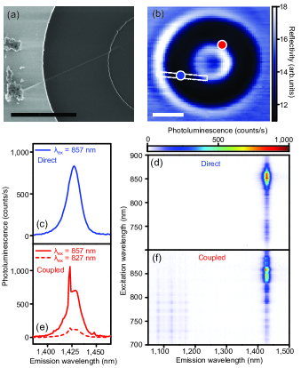
Surprisingly, the nanotube emission can also be observed at the opposite side of the disk [Fig. 3(e)], although it is spatially separated from the nanotube by 3 m. Notable is the sharp peak that appears on top of the nanotube spectrum. We identify this peak to be the 15th-order WGM with TE polarization [Fig. 2(b)]. As the mode wavelength corresponds to an energy far below the bandgap of Si, we attribute the emergence of this peak to nanotube emission coupled to a WGM.
The PLE map taken at the same position [Fig. 3(f)] resembles that of the directly measured nanotube [Fig. 3(d)], and in particular, the narrow WGM peak and the broader CNT emission peak are both maximized at the same excitation wavelength. This implies that the absorption characteristics are of the same origin for both WGM and CNT peaks, further supporting that the emission from the suspended nanotube is coupled to the WGM. We also note that faint Si emission is visible at wavelengths shorter than 1200 nm in Fig. 3(f). The contrast with bright CNT emission demonstrates the advantage of using direct-gap nanotube emitters.
Different from the direct measurement of the suspended CNT, the PLE map for coupled emission shows strong modulation of intensity with changes in the excitation wavelength. As mentioned previously, there exist WGMs at these wavelengths as well, and they can cause enhancements of the excitation efficiency when excitation is resonant with a WGM. When both the excitation and emission are in resonance with WGMs, we meet the doubly resonant condition of the cavity. Similar to the case of Si PL, the emission is enhanced by a factor of 10 at double resonance compared to off-resonant conditions [Fig. 3(e)], allowing non-local control over nanotube emission through spectral tuning.
The photons that couple to the WGM circulate within the microdisk, and this can be visualized through spectrally resolved PL imaging as in the case of WGM at Si emission wavelengths [Fig. 4(a)]. Using a higher resolution grating, we collect PL spectra as we raster the laser spot over the scan area, and fit them with two Lorentzian functions corresponding to the WGM peak and the direct CNT emission peak [Fig. 4(b)]. We find that the measured quality factor of the WGM is limited by spectrometer resolution to be 3000, which is already two orders of magnitude larger compared to a simple planar cavity.Xia et al. (2008) In Fig. 4(c) and 4(d), spectrally resolved PL images corresponding to the WGM and direct CNT emission are presented. It is clear that nanotube emission coupled to the WGM circulates within the disk and illuminates the circumference [Fig. 4(c)], showing that CNT emission is efficiently guided into the silicon photonic structure.
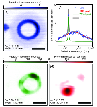
The direct emission from the CNT is centered on the nanotube itself as expected [Fig. 4(d)], although one can observe a lower intensity spot at the opposite side of the disk. We interpret the existence of such a remote spot in terms of in-plane Fabry-Perot mode within the microdisk.Mintairov et al. (2008) Such an interpretation is also consistent with the image of the WGM [Fig. 4(c)], which shows larger intensity near that spot.
Our results demonstrate the feasibility of integrating telecom-wavelength nanotube emitters in silicon photonics, opening up further possibilities for scaling down monolithic photonic circuits. By fabricating arrays of microdisks with different diameters and thus different resonant wavelengths, it should be possible to address each microdisk by tuning the excitation wavelength. Furthermore, the WGMs that couple to emission will also differ, which would be useful for implementing on-chip wavelength-division multiplexing. Integration of single photon emitting CNTs Högele et al. (2008); Walden-Newman, Sarpkaya, and Strauf (2012) with silicon photonics may open up new opportunities for quantum optics on a chip.Politi et al. (2008)
Acknowledgements.
The authors acknowledge support from SCOPE, KAKENHI (21684016, 23104704, 24340066, 24654084), Asahi Glass Foundation, KDDI Foundation, and the Photon Frontier Network Program of MEXT, Japan. The devices were fabricated at the Center for Nano Lithography & Analysis at The University of Tokyo.References
- Liang and Bowers (2010) D. Liang and J. E. Bowers, Nature Photon. 4, 511 (2010).
- Reed et al. (2010) G. T. Reed, G. Mashanovich, F. Y. Gardes, and D. J. Thomson, Nature Photon. 4, 518 (2010).
- Michel, Liu, and Kimerling (2010) J. Michel, J. Liu, and L. C. Kimerling, Nature Photon. 4, 527 (2010).
- Leuthold, Koos, and Freude (2010) J. Leuthold, C. Koos, and W. Freude, Nature Photon. 4, 535 (2010).
- O’Connell et al. (2002) M. J. O’Connell, S. M. Bachilo, C. B. Huffman, V. C. Moore, M. S. Strano, E. H. Haroz, K. L. Rialon, P. J. Boul, W. H. Noon, C. Kittrell, J. Ma, R. H. Hauge, R. B. Weisman, and R. E. Smalley, Science 297, 593 (2002).
- Weisman and Bachilo (2003) R. B. Weisman and S. M. Bachilo, Nano Lett. 3, 1235 (2003).
- Kong et al. (1998) J. Kong, H. T. Soh, A. M. Cassell, C. F. Quate, and H. Dai, Nature 395, 878 (1998).
- Misewich et al. (2003) J. A. Misewich, R. Martel, P. Avouris, J. C. Tsang, S. Heinze, and J. Tersoff, Science 300, 783 (2003).
- Chen et al. (2005) J. Chen, V. Perebeinos, M. Freitag, J. Tsang, Q. Fu, J. Liu, and P. Avouris, Science 310, 1171 (2005).
- Mann et al. (2007) D. Mann, Y. K. Kato, A. Kinkhabwala, E. Pop, J. Cao, X. Wang, L. Zhang, Q. Wang, J. Guo, and H. Dai, Nature Nanotech. 2, 33 (2007).
- Xia et al. (2008) F. Xia, M. Steiner, Y.-M. Lin, and P. Avouris, Nature Nanotech. 3, 609 (2008).
- Mueller et al. (2010) T. Mueller, M. Kinoshita, M. Steiner, V. Perebeinos, A. A. Bol, D. B. Farmer, and P. Avouris, Nature Nanotech. 5, 27 (2010).
- Lefebvre, Homma, and Finnie (2003) J. Lefebvre, Y. Homma, and P. Finnie, Phys. Rev. Lett. 90, 217401 (2003).
- Watahiki et al. (2012) R. Watahiki, T. Shimada, P. Zhao, S. Chiashi, S. Iwamoto, Y. Arakawa, S. Maruyama, and Y. K. Kato, Appl. Phys. Lett. 101, 141124 (2012).
- Gaufrès et al. (2012) E. Gaufrès, N. Izard, A. Noury, X. Le Roux, G. Rasigade, A. Beck, and L. Vivien, ACS Nano 6, 3813 (2012).
- McCall et al. (1992) S. L. McCall, A. F. J. Levi, R. E. Slusher, S. J. Pearton, and R. A. Logan, Appl. Phys. Lett. 60, 289 (1992).
- Borselli, Johnson, and Painter (2005) M. Borselli, T. Johnson, and O. Painter, Opt. Express 13, 1515 (2005).
- Soltani, Yegnanarayanan, and Adibi (2007) M. Soltani, S. Yegnanarayanan, and A. Adibi, Opt. Express 15, 4694 (2007).
- Michler et al. (2000) P. Michler, A. Kiraz, C. Becher, W. V. Schoenfeld, P. M. Petroff, L. Zhang, E. Hu, and A. Imamoğlu, Science 290, 2282 (2000).
- Peter et al. (2005) E. Peter, P. Senellart, D. Martrou, A. Lemaître, J. Hours, J. M. Gérard, and J. Bloch, Phys. Rev. Lett. 95, 067401 (2005).
- Mintairov et al. (2008) A. M. Mintairov, Y. Chu, Y. He, S. Blokhin, A. Nadtochy, M. Maximov, V. Tokranov, S. Oktyabrsky, and J. L. Merz, Phys. Rev. B 77, 195322 (2008).
- Moritsubo et al. (2010) S. Moritsubo, T. Murai, T. Shimada, Y. Murakami, S. Chiashi, S. Maruyama, and Y. K. Kato, Phys. Rev. Lett. 104, 247402 (2010).
- Yasukochi et al. (2011) S. Yasukochi, T. Murai, S. Moritsubo, T. Shimada, S. Chiashi, S. Maruyama, and Y. K. Kato, Phys. Rev. B 84, 121409(R) (2011).
- Hartschuh et al. (2003) A. Hartschuh, H. N. Pedrosa, L. Novotny, and T. D. Krauss, Science 301, 1354 (2003).
- Lefebvre et al. (2004) J. Lefebvre, J. M. Fraser, P. Finnie, and Y. Homma, Phys. Rev. B 69, 075403 (2004).
- Maruyama et al. (2002) S. Maruyama, R. Kojima, Y. Miyauchi, S. Chiashi, and M. Kohno, Chem. Phys. Lett. 360, 229 (2002).
- Ohno et al. (2006) Y. Ohno, S. Iwasaki, Y. Murakami, S. Kishimoto, S. Maruyama, and T. Mizutani, Phys. Rev. B 73, 235427 (2006).
- Högele et al. (2008) A. Högele, C. Galland, M. Winger, and A. Imamoğlu, Phys. Rev. Lett. 100, 217401 (2008).
- Walden-Newman, Sarpkaya, and Strauf (2012) W. Walden-Newman, I. Sarpkaya, and S. Strauf, Nano Lett. 12, 1934 (2012).
- Politi et al. (2008) A. Politi, M. J. Cryan, J. G. Rarity, S. Yu, and J. L. O’Brien, Science 320, 646 (2008).