Genetic Design of Enhanced Valley Splitting towards a Spin Qubit in Silicon
Electronic spins in Silicon (Si) are rising contenders for qubits – the logical unit of quantum computation Nielsen and Chuang (2000) – owing to its outstanding spin coherence properties and compatibility to standard electronics Morton et al. (2011); Zwanenburg et al. (2012). A remarkable limitation for spin quantum computing in Si hosts is the orbital degeneracy of this material’s conduction band, preventing the spin- states from being an isolated two-level system Koiller et al. (2001); Zwanenburg et al. (2012). So far available samples of Si quantum wells cladded by Ge-Si alloy barriers provide relatively small valley splitting (VS), with the order of 1 meV or less Nicholas et al. (1980); Lai et al. (2006); Goswami et al. (2007); Boykin et al. (2004); Friesen et al. (2007); Saraiva et al. (2009), degrading the fidelity of qubits encoded in spin “up” and “down” states in Si. Here, based on an atomically resolved pseudopotential theory, we demonstrate that ordered Ge-Si layered barriers confining a Si slab can be harnessed to enhance the VS in the active Si region by up to one order of magnitude compared to the random alloy barriers adopted so far. A biologically inspired genetic-algorithm search Franceschetti and Zunger (1999); Piquini et al. (2008) is employed to identify magic Ge/Si layer sequences of the superlattice barriers that isolate the electron ground state in a single valley composition with VS as large as 9 meV. The enhanced VS is preserved with the reasonable inter-layer mixing between different species, and is interestingly “protected” even if some larger mixing occurs. Implementation of the optimized layer sequences of barriers, within reach of modern superlattice growth techniques Menczigar et al. (1993), overcomes in a practical systematic way the main current limitations related to the orbital degeneracy, thus providing a roadmap for reliable spin-only quantum computing in Si.
The qubits for quantum information processing are encoded in two-level quantum systems , and can be realized, for example, by two spin states of an electron at the conduction band edge of a semiconductor Loss and DiVincenzo (1998); Kane (1998). While Si enjoys a number of advantages over III-V semiconductors in this respect, including long spin coherence lifetime (associated with its weak spin-orbit coupling and small content of nonzero-nuclear-spin isotopes), as well as advanced fabrication know-how, its major drawback is the (six-fold) orbital degeneracy of its lowest conduction band (Fig. 1a) located close to the point in the Brillouin zone. This is no longer a two-level system determined solely by its spin, leading to considerable leakage and decoherence driven by the energetic proximity among the degenerate orbitals Koiller et al. (2001). Whereas this six-fold valley degeneracy in the Oh-symmetric bulk Si can be partially removed by application of tensile biaxial strain Schäffler (1997), thus, isolating the two lowest and components from the rest (Fig. 1b), the creation of a sufficiently large energy splitting within this -valley subspace (hereby called valley splitting (VS), see Fig. 1c) has proven to be a challenge for the experimental realization of Si-based spin qubits Zwanenburg et al. (2012).
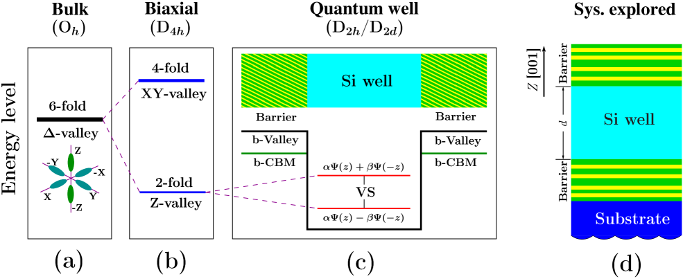
The geometry of the basic physical system explored (Fig. 1d) includes a Si slab (“Well”) interfaced by a material with higher conduction band (“barrier”). The VS of this system depends on a multitude of degrees of freedom present in the realistic device growth. The Si well of thickness cladded by barrier materials of composition is coherently strained on a substrate with the planar lattice constant (determined by its composition ). We focus on the substrate and barrier composed of Ge-Si based materials, which provide better-quality interfaces than oxides. The barrier can be a Ge-Si random alloy of composition or any corresponding atomistically ordered structure. We incorporate monolithically the full system containing up to 105 atoms/computational-cell, via an atomistic pseudopotential Hamiltonian A. Zunger (1996); Wang and Zunger (1995), solved in a plane-wave basis for each relaxed atomic configuration, which gives directly the energies {} and wavefunctions {} of the valley states.
Macroscopic degrees of freedom: We start by exploring the continuum configuration-averaged degrees of freedom in this system, as common in the literature Boykin et al. (2004); Nestoklon et al. (2006); Friesen et al. (2007); Valavanis et al. (2007); Boykin et al. (2008); Saraiva et al. (2009), finding that whereas they do not provide a clear avenue to major VS enhancement, their exploration hints at the importance of another length scale. We consider a fixed-thickness Si well embedded in the Ge-Si alloy barriers with varied composition , on three substrates with different composition . For each alloy composition of barriers, we calculated 20 randomly realized atomic configurations and the averaged VS is evaluated. The solid red line in Figs 2a-c shows the calculated configuration-averaged VS as a function of composition . Generally, one observes an uneventful monotonic increase of the averaged VS as the barrier becomes richer in Ge (see also Supplementary Fig. S1b, which shows the VS for a few distinct ). Such continuum-like effect of the configuration-averaged alloy barriers can be understood by the gradual change of the barrier height, i.e., the band offset between the valley states of Si well and barrier (“b-Valley” in Fig. 1c and Supplementary Fig. S1a) Saraiva et al. (2009, 2011). Although the averaged VS (red lines in Figs 2a-c) shows substantial dependence on the epitaxial strain (also see Supplementary Fig. S1b), the variation of the macroscopic barrier composition and substrate composition provides limited tuning of VS.

Atomically resolved length scale: Important clues emerge as to the significance of the atomically resolved length scale and symmetry, as indicated in a recent work on the intervalley splittings of PbSe Poddubny et al. (2012). In principle, the splitting within the valleys is closely related to the interface-induced deviation from the Oh symmetry of bulk Si (or the D4h symmetry of biaxially strained Si). For a Si quantum well (Fig. 1d), the interfacial perturbation potential with the D2h/D2d symmetry provides a coupling channel between two -valley states, giving a VS magnitude in perturbation theory of . To tune VS, we can engineer the magnitude and profile of the perturbation potential by varying the atomic-scale structure and symmetry for the well and barriers. The importance of the atomic scale is revealed, for example, in Fig. 2a-c, where the blue circles represent the VS obtained by resolving distinct random realizations of site occupations in alloy barriers. The VS ranging from 0 to an upper bound of 1 meV is in reasonable agreement with experiments Nicholas et al. (1980); Lai et al. (2006); Goswami et al. (2007); Zwanenburg et al. (2012). We can see that the VS of Si can vary significantly for different atomic configurations of barriers at the same composition . This is consistent with the recent calculation showing that specific atomic arrangements at the interface region can result in distinct VS (however the assumed Si3Ge luzonite structure is difficult for experimental realization) Jiang et al. (2012). Also, the critical role of atomic resolution and symmetry is apparent by considering a system of short-period Si-Ge superlattices located directly on a substrate (i.e, no active Si layer in Fig. 1d), where our calculated VS reaches values as large as several tens of meV, although the Si-Ge superlattice system is not the case of interest here (but may relate to different qubit proposals Vrijen et al. (2000)).
Inspired by these basic insights from the atomic length scale, we next explore in a systematic way whether and how atomic degrees of freedom in the Si well, barrier composition and structure, and epitaxial substrate could raise the VS. By varying the above degrees of freedom, we aim at identifying the rule of how the relevant physical factors govern VS, and use it to seek an optimized VS.
Effect of Si well thickness: The thickness of the Si well is the first obvious parameter to tune the perturbation potential , and thus manipulate VS. Fig. 3a shows the dependence of VS on the thickness in monolayers (MLs) for fixed pure Ge barrier from the pseudopotential calculations. We observe an overall decay in the magnitude of VS as the thickness increases, while the VS for with an odd (blue circles) and even (red squares) number of MLs appears to oscillate independently, with a common period 14 ML and a phase shift of /2. This intriguing oscillatory behavior has been reported previously, and was attributed to the symmetry change of the Si well of MLs: D D2h for odd even Boykin et al. (2004); Nestoklon et al. (2006); Srinivasan et al. (2008).
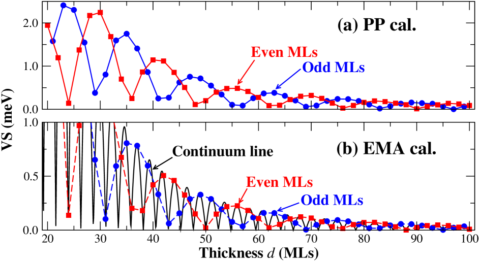
In Fig. 3b, we show the calculated VS within the effective mass approximation (EMA) as a function of the continuum thickness (solid black line), as well as the data sampled at odd (blue circles) and even (red squares) atomic MLs. We find that while the EMA results with continuum show a much faster oscillation, clearly they reproduce well the existence of “independent” oscillation for discrete of odd and even MLs. Thus, we attribute this atomic-scale odd-even independent oscillation to a manifestation of the aliasing effect (introduced by sampling a function at a rate which is not fine enough to capture each oscillation), rather than to a symmetry change (see Supplementary Information for detailed description). This understanding underlines that to gain an optimized VS of Si well, a well-controlled growth of monolayer precision is required to reach the thickness at the peak of the oscillation.
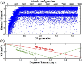
Atomically ordered superlattices barriers: The substantial effect of specific atomic realization for the disordered alloy barriers (open circles in Figs 2a-c) stimulates us to investigate the situation where the barriers are composed of ordered superlattices, i.e., a repeated sequence of Si and Ge layers of arbitrarily assigned widths. We explore the system composed of a 40 MLs Si well (located at an even peak of Fig. 3a) embedded in the superlattice barriers with a period of 80 MLs (with the minimum stacking unit of bilayer to comply with current experimental growth conditions). This gives an astronomical number (240) of candidate layer-stacking configurations of barriers, so a direct calculation for enumeration of all the candidates is not practical. We perform an inverse-band-structure search calculation Franceschetti and Zunger (1999); Piquini et al. (2008) where the best fitness is defined by the maximum VS, and favorable structures are selected within a genetic algorithm approach. Fig. 4a shows the evolution of fitness (VS) with generation (evolution step). One clearly observes that the VS can be effectively tuned within a wide energy range, from negligibly small up to 9 meV, by varying Ge/Si stacking sequence of superlattice barriers. Less than 100 generations already identify the best individuals, which remain superior for the following hundreds of generations, while new individuals still emerge with intermediate VS values.
Figs 2d-f show the achieved VS of all the atomic configurations visited by the inverse-band-structure search, sorted in terms of the Ge content in the barriers on three varied substrates. It is demonstrated that a remarkable VS enhancement by a factor of 5-10 is achievable with ordered superlattice barriers as compared to disordered alloy barriers (Figs 2a-c) for all substrates. Particularly, comparing with the maximum VS for the disordered alloy barriers – 1.0 meV on all the substrates, the maximum VS (accompanied by the optimum configuration) for the ordered superlattice barriers reaches:
0 Ge substrate: 5.7 meV (Ge4Si4Ge2Si6Ge4Si4Ge4Si);
20 Ge substrate: 7.4 meV (Ge4Si4Ge4Si2Ge4Si6Ge4Si);
40 Ge substrate: 8.7 meV (Ge4Si6Ge2Si6Ge4Si4Ge4Si).
We find that the multilayer superlattice barriers show larger VS around the central region, i.e., at 40-60 Ge content in the barrier, different from higher Ge content leading to larger VS for random alloy barriers. The same Ge content in the superlattice barriers can lead to both high and low VS extremes, again emphasizing the key role of atomistic scale ordering in controlling VS.
The Si/Ge4 motif: Interestingly, all the optimum configurations identified start the barrier sequence by a Ge4 sub-layer. This same“magic” thickness for the first Ge sub-layer is also identified in the exhaustive enumeration calculations for the superlattice barriers with a shorter period of 16 MLs (see Supplementary Fig. S2a-c). Similar results are obtained for a Si well with the thickness of 47 MLs (located at an odd peak of Fig. 3a, see Supplementary Fig. S2d-f). In order to better understand this, we explore a simple case – the fixed 40 MLs Si well embedded in GenSin superlattice barriers with = 1, 2, 4, 8, 16, as shown in Fig. 5a. We see that the barrier of Ge4Si4 superlattice indeed exhibits the largest VS (7 meV), whereas all other barriers (including pure Ge) show typically low VS ( meV). This indicates that the starting sub-layer thinner or thicker than Ge4 seem to equally suppress VS. We unravel the underlying origin within the EMA context. Briefly, the VS induced by a Si/Ge (ascending offset) interface has opposite sign to the Ge/Si (descending offset) interface with the same wavefunction. Choosing the interface positions to match the maxima/minima of the VS at the ascending/descending interfaces would maximize the total VS. It is impossible to match the interface positions perfectly to the incommensurate oscillations of well-thickness dependent VS (Fig. 3), but the Ge4 sub-layer is the closest we can get to this matching. Conversely, starting with a Ge2 sub-layer cladding the Si well, we find a destructive interference, in agreement with the suppressed VS for Si2Ge2 superlattice barrier in Fig. 5a. This engineering is analogous to that of a distributed Bragg reflector (see Supplementary Information for detailed description). But the fact that the oscillations are incommensurate with the lattice and the strong dependence of VS on atomic ordering makes it impossible to analytically predict the optimal structure. For this reason, the genetic selection of candidate structures is an essential ingredient of this work.
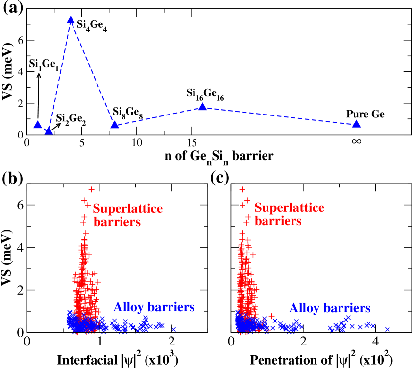
Previous studies correlate the VS with the electronic wave-function magnitude of the valley at the interface (interfacial ) Nestoklon et al. (2006); Friesen et al. (2007); Saraiva et al. (2009, 2011) and the wave-function penetration into the barrier region (penetration of ) Saraiva et al. (2009, 2011). In Fig. 5b and 5c, we probed the VS as a function of interfacial and penetration of , for the 40 MLs Si well cladded by alloys barriers (blue crosses) and superlattice barriers (red pluses). Compared with the alloy barriers, the stronger confinement power of superlattice barriers give much narrower distribution of both interfacial and penetration of . The optimum VS values for the superlattice barriers emerge in the region of the narrowest distribution of these two quantities. This is related to the sharp well/barrier interface for superlattice barriers, which could in principle enhance the VS Saraiva et al. (2009); Culcer et al. (2010).
Effect of Ge-Si intermixing in barriers: Since it is still a challenge to grow perfectly pure sub-layer of Si or Ge in superlattices due to atomic inter-diffusion Menczigar et al. (1993), we examine how much VS is affected by the interfacial mixing between Si and Ge. In particular, the inter-layer mixing is modeled by mapping pure Si into Si1-ηGeη, and pure Ge into Ge1-ηSiη at the interfacial first few layers, determined by a mixing length. The parameter quantifies the degree of inter-layer mixing, with = 0 corresponding to no mixing and = 0.5 meaning maximum mixing, i.e., complete destruction of Si-rich or Ge-rich pattern within this layer. Fig. 4b shows the calculated VS as a function of for the above optimized superlattice barrier on 40 Ge substrate (Ge4Si6Ge2Si6Ge4Si4Ge4Si, see Supplementary Fig. S3 for more ordered superlattice barriers), when two cases of mixing lengths [2 MLs (green) and 4 MLs (red)] are explored. Note that the favorable Ge4 starting sub-layer is only partially damaged if the mixing length is 2 ML (1 ML towards each side of the interface), while for the 4ML mixing length the Ge-pure layer is totally destroyed. The non-trivial, non-monotonic behavior indicates that the intermixing may lead to the formation of a more complex geometry which tunes VS by affecting the interference pattern discussed before. This is reflected in a surprisingly steeper suppression of VS in the shorter mixing length of 2 MLs compared to the longer mixing length of 4 MLs for small . Similarly, at very large , the structure becomes a complex layering of alloys, pure Si and pure Ge, which might keep suppressing (the case of 4ML) or invert the symmetry and enhance the VS (the case of 2ML). In both mixing lengths, for a reasonable degree of mixing ( 0.1), the rather high VS of 6 meV is preserved.
Advantage of atomically ordered barriers: We anticipate that the choice of ordered superlattice barriers instead of random alloy barriers might mitigate many problems of real samples. For instance, the intrinsic non-deterministic nature of alloys induces disorder ranging from the geometry of the interface plane to the inhomogeneous strain fields Evans et al. (2012). The leakage of electrons tunneling through the superlattice barrier should also be reduced since the electronic density inside the barrier is much reduced. Our atomically-resolved pseudopotential calculations of the Si well strained on various substrates and interfaced with different barriers can be used to explore the effects on VS of both global macroscopic quantities (strain, alloy compositions, geometric well thickness), as well as atomic scale effects (ordering, inter-layer mixing, even-odd independent oscillation). We identify the critical Si well thicknesses as well as an emerging “magic” motif of starting in the ordered superlattice barrier that causes strong coupling between and valley states, leading to significantly enhanced VS as large as 9 meV. The predicted structure is accessible within current experimental fabrication capabilities. This opens the way to fundamental understanding of the hitherto rather intangible -valley splitting in indirect-gap semiconductors such as Si with the possible benefit of isolating single electron valley state for spin-based quantum computing.
Methods
The structures employed to optimize VS in this work (Fig. 1d) involve an active Si well with the thickness of MLs, cladded on both sides by a barrier consisting of Si-Ge based materials, including homogeneous random alloy and layer-by-layer superlattice structures. The whole system is coherently strained on a substrate, via minimization of atomically-resolved strain with a generalized valence force field method (see Supplementary Methods A) Bernard and Zunger (1991). To comply with what is currently accessible in experimental growth we used two restrictions: (i) Since too high Ge content in substrate is known to cause dislocations in thick Si active layers to relieve excessive strain, up to 40 Ge content is considered in substrate. (ii) a bilayer is used as the minimum stacking unit of each specie (Si/Ge) for the superlattice barrier.
The energies and wave-functions of conduction valley states for candidate structures are calculated “on the fly” with the atomistic pseudopotential method, described in detail in Refs. Wang and Zunger (1995); A. Zunger (1996). The atomistic pseudopotential method (overcoming the well-known Density-Functional-Theory limitations on electronic structure calculations), accompanied with a plane-wave basis set and folded-spectrum diagonalization, allow us to accurately calculate energy splitting of -valley states (at the order of meV or lower) for numerous candidate structures with economic efficiency, as described in Supplementary Methods B.
Effective mass approach calculations were performed to accompany the interpretation of the pseudopotential results. The effective mass calculations follow essentially the model presented in Refs. Saraiva et al. (2009, 2011), adapted to describe quantum wells in first order approximation, as described briefly in Supplementary Methods C.
For Si wells embedded in layer-by-layer superlattice barriers, since the search space shows a combinatorial burst of degrees of freedom, we employ the developed inverse-band-structure approach Franceschetti and Zunger (1999); Piquini et al. (2008); d’Avezac et al. (2012), i.e., a biologically inspired (Darwinian) genetic algorithm to guide the electronic structure calculations, with the aim at finding the optimum configuration that gives the maximum VS (Supplementary Methods D).
Acknowledgements
We thank M. A. Eriksson and M d’Avezac for helpful discussions. This work is supported by the U.S. Department of Energy, Office of Science, Basic Energy Sciences, under Contract No. DE-AC36-08GO28308 to NREL. The ”Center for Inverse Design” is a DOE Energy Frontier Research Center. A.S. and B.K.’s work is part of the Brazilian National Institute for Science and Technology on Quantum Information. A.S. and B.K. acknowledge partial support from FAPERJ, CNPq and CAPES.
References
- Nielsen and Chuang (2000) M. A. Nielsen and I. L. Chuang, Quantum Computation and Quantum Information (Cambridge University Press, 2000), ISBN 9780521635035.
- Morton et al. (2011) J. J. L. Morton, D. R. McCamey, M. A. Eriksson, and S. A. Lyon, Nature 479, 345 (2011), ISSN 0028-0836, URL http://www.nature.com/nature/journal/v479/n7373/abs/nature10681.html.
- Zwanenburg et al. (2012) F. A. Zwanenburg, A. S. Dzurak, A. Morello, M. Y. Simmons, L. C. L. Hollenberg, G. Klimeck, S. Rogge, S. N. Coppersmith, and M. A. Eriksson, arXiv:1206.5202 (2012), URL http://arxiv.org/abs/1206.5202.
- Koiller et al. (2001) B. Koiller, X. Hu, and S. Das Sarma, Physical Review Letters 88, 027903 (2001), URL http://link.aps.org/doi/10.1103/PhysRevLett.88.027903.
- Nicholas et al. (1980) R. Nicholas, K. von Klitzing, and T. Englert, Solid State Communications 34, 51 (1980), ISSN 0038-1098, URL http://www.sciencedirect.com/science/article/pii/0038109880906286.
- Lai et al. (2006) K. Lai, T. M. Lu, W. Pan, D. C. Tsui, S. Lyon, J. Liu, Y. H. Xie, M. Mühlberger, and F. Schäffler, Phys. Rev. B 73, 161301 (2006), URL http://link.aps.org/doi/10.1103/PhysRevB.73.161301.
- Goswami et al. (2007) S. Goswami, K. A. Slinker, M. Friesen, L. M. McGuire, J. L. Truitt, C. Tahan, L. J. Klein, J. O. Chu, P. M. Mooney, D. W. van der Weide, et al., Nature Physics 3, 41 (2007).
- Boykin et al. (2004) T. B. Boykin, G. Klimeck, M. A. Eriksson, M. Friesen, S. N. Coppersmith, P. von Allmen, F. Oyafuso, and S. Lee, Applied Physics Letters 84, 115 (2004).
- Friesen et al. (2007) M. Friesen, S. Chutia, C. Tahan, and S. N. Coppersmith, Physical Review B 75, 115318 (2007), URL http://link.aps.org/doi/10.1103/PhysRevB.75.115318.
- Saraiva et al. (2009) A. L. Saraiva, M. J. Calderón, X. Hu, S. Das Sarma, and B. Koiller, Phys. Rev. B 80, 081305 (2009), URL http://link.aps.org/doi/10.1103/PhysRevB.80.081305.
- Franceschetti and Zunger (1999) A. Franceschetti and A. Zunger, Nature 402, 60 (1999).
- Piquini et al. (2008) P. Piquini, P. A. Graf, and A. Zunger, Physical Review Letters 100, 186403 (2008).
- Menczigar et al. (1993) U. Menczigar, G. Abstreiter, J. Olajos, H. Grimmeiss, H. Kibbel, H. Presting, and E. Kasper, Physical Review B 47, 4099 (1993), URL http://link.aps.org/doi/10.1103/PhysRevB.47.4099.
- Loss and DiVincenzo (1998) D. Loss and D. P. DiVincenzo, Physical Review A 57, 120 (1998), URL http://link.aps.org/doi/10.1103/PhysRevA.57.120.
- Kane (1998) B. E. Kane, Nature 393, 133 (1998), ISSN 0028-0836, URL http://www.nature.com/nature/journal/v393/n6681/abs/393133a0.html.
- Schäffler (1997) F. Schäffler, Semiconductor Science and Technology 12, 1515 (1997), ISSN 0268-1242, 1361-6641, URL http://iopscience.iop.org/0268-1242/12/12/001.
- A. Zunger (1996) A. Zunger, in Quantum Theory of Real Materials, edited by J. R. Chelikowsky and S. G. Louie (Kluwer Academic Publishers, Boston, MA, 1996), pp. 173–187.
- Wang and Zunger (1995) L.-W. Wang and A. Zunger, Physical Review B 51, 17398 (1995), URL http://link.aps.org/doi/10.1103/PhysRevB.51.17398.
- Nestoklon et al. (2006) M. O. Nestoklon, L. E. Golub, and E. L. Ivchenko, Phys. Rev. B 73, 235334 (2006), URL http://link.aps.org/doi/10.1103/PhysRevB.73.235334.
- Valavanis et al. (2007) A. Valavanis, Z. Ikonić, and R. W. Kelsall, Phys. Rev. B 75, 205332 (2007).
- Boykin et al. (2008) T. B. Boykin, N. Kharche, and G. Klimeck, Phys. Rev. B 77, 245320 (2008).
- Saraiva et al. (2011) A. L. Saraiva, M. J. Calderón, R. B. Capaz, X. Hu, S. Das Sarma, and B. Koiller, Phys. Rev. B 84, 155320 (2011).
- Poddubny et al. (2012) A. N. Poddubny, M. O. Nestoklon, and S. V. Goupalov, Phys. Rev. B 86, 035324 (2012), URL http://link.aps.org/doi/10.1103/PhysRevB.86.035324.
- Jiang et al. (2012) Z. Jiang, N. Kharche, T. Boykin, and G. Klimeck, Applied Physics Letters 100, 103502 (2012), URL http://link.aip.org/link/?APL/100/103502/1.
- Vrijen et al. (2000) R. Vrijen, E. Yablonovitch, K. Wang, H. W. Jiang, A. Balandin, V. Roychowdhury, T. Mor, and D. DiVincenzo, Physical Review A 62, 012306 (2000), URL http://link.aps.org/doi/10.1103/PhysRevA.62.012306.
- Srinivasan et al. (2008) S. Srinivasan, G. Klimeck, and L. P. Rokhinson, Applied Physics Letters 93, 112102 (2008), URL http://link.aip.org/link/?APL/93/112102/1.
- Culcer et al. (2010) D. Culcer, X. D. Hu, and S. Das Sarma, Physical Review B 82 (2010).
- Evans et al. (2012) P. G. Evans, D. E. Savage, J. R. Prance, C. B. Simmons, M. G. Lagally, S. N. Coppersmith, M. A. Eriksson, and T. U. Schuelli, Advanced Materials 24, 5217 (2012).
- Bernard and Zunger (1991) J. E. Bernard and A. Zunger, Phys. Rev. B 44, 1663 (1991).
- d’Avezac et al. (2012) M. d’Avezac, J.-W. Luo, T. Chanier, and A. Zunger, Physical Review Letters 108, 027401 (2012), URL http://link.aps.org/doi/10.1103/PhysRevLett.108.027401.