Tailoring the diameter of decorated C N nanotubes by temperature variations using HF-CVD
Abstract
Patterned films of decorated nitrogenated carbon (C N) nanotubes were catalytically synthesised by hot filament chemical vapour deposition (HF-CVD) in a nitrogen methane ammonia environment. The systematic study of a transition between different kinds of C N nanostructures as a function of the local substrate temperature ranging from 700 up to 820∘C is presented. The morphology, the diameter as well as the properties of the generated tubular structures showed strong dependence on this parameter. By means of electron microscopy a new type of decoration covering all tubular structures was observed. Buckled lattice fringes revealed the disordered graphitic-like character of the hollow C N nanotubes. Raman spectroscopy confirmed a transition in the microscopic order as a function of temperature. Furthermore field emission in vacuum was studied and showed a spectacular correlation to the deposition temperature and therefore the diameter of the C N tubes. For arrays of tubes thinner than 50 nm an onset field below 4 V/m was observed.
Introduction
The discovery of fullerene C60 by Kroto et al. in 1985 1 has sparked a lot of exciting research in the field of carbon based nanostructures. Numerous new structures like carbon nanotubes 2 , nano-onions 3 , nano-horns 4 or micro-trees 5 were reported. Most of these materials hold a variety of interesting properties including electronic 6 ; 7 and mechanical properties 8 ; 9 , which promise to be not just of academic interest but also to be sources for new applications. As an example carbon single and multiwalled nanotubes have been used as cold field emitters (e.g. 10 ) and as hydrogen storage material 11 .
On the other hand, carbon nitride (CNx) coatings and diamond like carbon (DLC) films have been under intense investigation for a longer time because they can serve as hard layers for tools (e.g. 12 ). Interesting mechanical behaviour, in particular an exceptionally high elasticity, has also been observed for sputtered CNx thin solid films 13 ; 14 . In that case, the strengthening effect has been attributed to a cross-linked fullerene-like structure with curved and buckled basal planes 13 .
Furthermore, doping of carbon nanotubes with nitrogen or boron is expected to induce exciting electronic properties 15 . Miyamoto et al. 16 showed that tubular forms of graphitic-like carbon nitrides can be stabilised by displacing C atoms out of the honeycomb network of graphite. Detailed transmission electron microscopy (TEM) and electron energy loss spectroscopy (EELS) of carbon nitride nanotubulites prepared by chemical vapour deposition (CVD) and magnetron sputtering, respectively, was reported by Suenaga et al. 17 ; 18 . Several other groups have also succeeded in synthesising nitrogen-containing nanotubes 19 ; 20 ; 21 ; 22 ; 23 . Furthermore, nanotubes within the boron nitride (BN) 23 ; 24 and ternary B-C-N systems 22 ; 25 ; 26 have been reported. Apart from the structure, both the electronic and mechanical properties are dependent on the chemistry of hetero-atomic nanotubes (e.g. 27 ). However, the correlation between the morphology, crystalline order and properties of such tubular CNx structures is not yet completely understood.
Recently we described the autocatalytic growth of a new type of carbon structures 28 produced by hot filament chemical vapour deposition (HF-CVD). They consist of tubular nitrogenated carbon (C-N) nanostructures covered with graphitic-like sheets growing perpendicular to the tube axis. Furthermore the essential role of nitrogen on structure formation of decorated nanotubes was analysed in detail by TEM and EELS 29 . At this stage various decorated nanotube-like structures were grown randomly distributed at the surface of a pure Si substrate, and factors that influence nucleation were not understood. Vapour-phase deposition of CNx nanotubes with controlled structure and chemical composition can provide a tool for synthesis of materials with tailored electronic 16 and mechanical properties 30 .
We present here a systematic study of the transition between different kinds of C-N nanostructures as a function of temperature (given by lateral distance from filament), which determines the tube diameter. Strong correlation to properties such as Raman signal and field emission were found. The fundament of these investigations was the deposition of patterned films of decorated nanotubes, which were realised by applying a catalyst on the substrate using the microcontact (CP) printing method.
Experimental methods
Synthesis of nanostructured material
Microcontact printing (CP) of catalysts 31 is becoming a popular method because it allows to form chemical patterns on the surface of a variety of substrates. Structured stamps were realised by curing the elastomer poly(dimthyl)siloxane (PDMS) over a master. They were then hydrophilised by an oxygen plasma treatment and stored under water to keep them hydrophilic. The stamps were dried under nitrogen flow for 10 s before use. The catalyst ink solution (Fe(NO3)3 9H2O and Ni(NO3)2 6H2O solved in ethanol) was applied to the stamps after a period of 12 h of ageing, which was found to be ideal for catalytic growth of nanotubes 32 . The printing was done by bringing the inked stamp in contact with the surface of a Si wafer for 3 s.
Decomposition of methane (CH4) using the bias-enhanced hot filament chemical vapour deposition technique results in a new type carbon based nanostructures. Pure nitrogen was used as dilution gas and a small flow of ammonia (NH3) was introduced during the experiments in order to increase the amount of nitrogen in the deposits. The total gas flow was kept constant at 500 sccm and a typical flow ratio of N2-CH4-NH3 of 100:1:1 was applied.
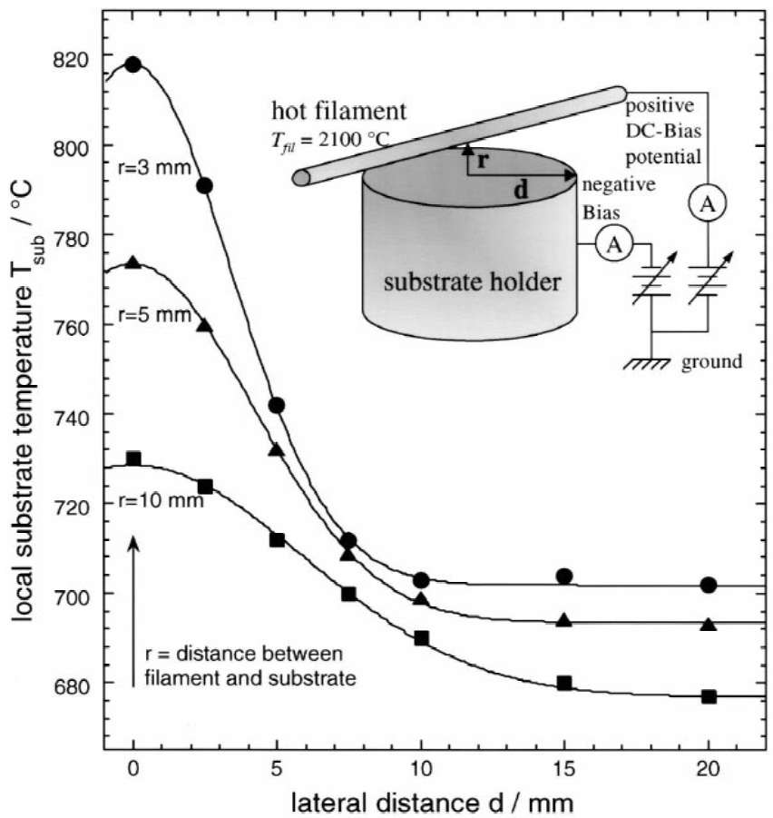
For all the experiments described in this work, only one resistively heated tungsten carbide (WC) filament ( = 500 m) was used in order to study the resulting nonuniformity in deposition conditions described by the lateral distance at the sample surface measured perpendicular to the filament. The inset in Fig. 1 shows schematically the experimental setup. A molybdenum (Mo) substrate holder placed at = 3 mm (fixed value for all further reported results) underneath the filament was heated independently to 650∘C. Positive and negative dc-bias potential up to 200 V were applied independently to the filament and to the substrate, respectively. The background pressure typically reached in the deposition chamber was 10-5 Pa, whereas the working pressure was kept constant at 300 Pa during deposition. A fixed filament temperature Tfil = 2100∘C as measured by means of a two-colour pyrometer was used. The temperature profile at the sample surface (Tsub versus ) as measured by a W-5%Re/W-26%Re thermocouple is given in Fig. 1. Due to the thermal radiation a strong temperature gradient was observed depending on the distance between filament and substrate (). The measurement data were fitted assuming a Gaussian distribution.
Characterisation techniques
Scanning electron microscopy (SEM) was performed to analyse the microstructures in plan view. A Philips XL 30 microscope equipped with a field emission gun (FEG) operating at an acceleration voltage between 2 and 5 kV, a working distance of typically 10 mm, and in secondary electron (SE) image mode was used.
The growth morphology of the tubular structures and their crystallinity were controlled by analytical transmission electron microscopy (TEM). For this purpose a Hitachi HF-2000 field emission microscope equipped with a Gatan image plate operating at 200 kV (point resolution 0.23 nm) was used.
The micro Raman technique was used to obtain local information about the vibrational properties of the nanostructures. The Raman spectra were recorded in backscattering configuration using the 514.5 nm line of an Ar+ ion laser and a DILOR XY 800 spectrometer. An incident maximal laser power of 20 mW was applied in order to avoid peak shifts due to thermal heating during data acquisition or structure transformations. A spot size of approximately 10 m was achieved with a 100 Olympus microscope objective. The spectra were calibrated using a natural diamond single crystal.
Additionally, field emission measurements were performed using the examined samples as cathodes with a lateral resolution of 1 mm. The emitted electrons were collected on a highly polished stainless steel spherical counterelectrode of 1 cm diameter, which corresponds to an emission area of 0.007 cm2. The distance was initially adjusted to 125 m and was reduced to 50 or 25 m when no emission was observed below 1000 V. A Keithley 237 source-measure unit was used for sourcing the voltage (up to 1000 V) and measuring the current with pA sensitivity, allowing the characterisation of current-voltage (I-V) behaviour.
Results
Morphology
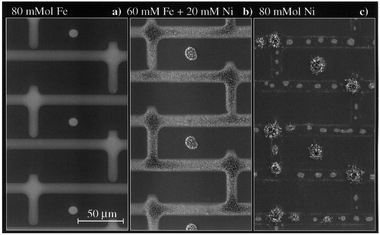
We used CP to study the specific effect of the catalyst on both the quality of the printed pattern and the tube growth. Figure 2 shows SEM images of the substrate after deposition using various catalyst mixtures. The structure consists of lines and dots with a typical structure width of 10 m. Best printing was achieved with an Fe catalyst as shown in Fig. 2(a) whereas the pure Ni solution showed poor printing behaviour. The Ni ink produced small drops on the stamp of 10 m diameter, which were transferred to the substrate as seen in Fig. 2(c). In contrast, a higher efficiency regarding the growth of nanotubes was obtained for Ni than for pure Fe. The best results in terms of both tube growth and patterns uniformity were achieved using an ethanolic ink containing 60 mMol Fe3+ and 20 mMol Ni2+. This ink was used for the following experiments. Note that the same type of decorated tubes also grows autocatalytically 28 with the disadvantage of a random distribution on the surface of a pure Si wafer. Clearly, a well-controlled film growth requires the use of a catalysts.
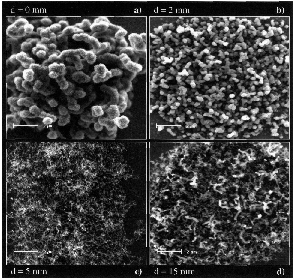
The above mentioned temperature gradient Tsub versus the lateral distance from the filament (Fig. 1) strongly affects the growth conditions for the nitrogenated carbon tubes. The evolution of the morphology of various tubular structures grown onto the substrate in dependence of this important parameter is represented in Fig. 3 by a series of SEM images. For Figures 3(a) to 3(d) the lateral distance d increases from 0 to 2, 5, and 10 mm, respectively. From = 0 to 5 mm (Figs. 3(a-c)) the structures become finer, i.e. the tube diameter decreases from approximately 1 m to 50 nm. Above = 10 mm the local substrate temperature remains constant at Tsub 700∘C (Fig. 1). Simultaneously a significant change in the morphology of the grown tubes is observed. As one can conclude from Fig. 3(d) nanotubes with a strong dispersion in diameter (20 to 200 nm) were formed at the same location, i.e. under the same conditions. In contrast, for higher Tsub ( 7 mm) a sharper local distribution of tubular C-N species in terms of tube diameter was obtained (Fig. 3(a-c)).
As a rule, all structures are of wounded tubular character. It is interesting to note that a decoration is formed over the surface of all studied tubes, which can be clearly seen in Fig. 3a. The large dendritic-like surface of the decorated C-N tubes results from thin foils or lamellae growing perpendicular to the tube axis. The shape of these nanoaggregates varies with the applied filament temperature, ranging from twisted lamellae to straight sheets showing ramifications 33 . Recently, we could show 29 that coiling as well as decoration depends on the amount of nitrogen incorporated in the tubes. Performing energy electron loss spectroscopy (EELS) a maximum N/C atomic ratio of 0.043 0.014 was obtained on samples produced under the same conditions but without catalyst 34 .
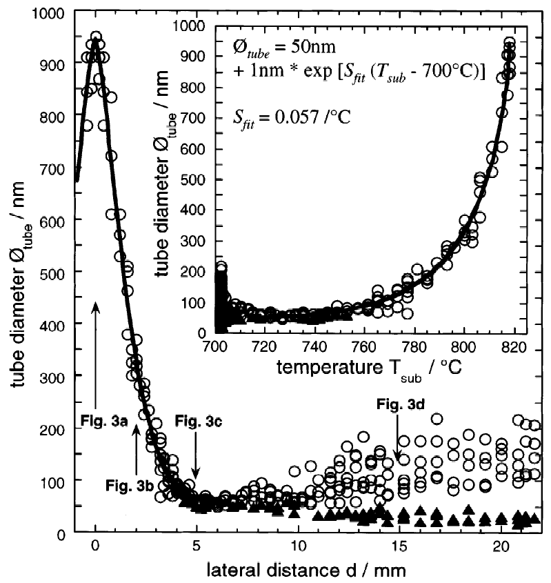
A quantitative analysis of the tube diameter () was done using high-magnification SEM. Figure 4 shows the observed data of the outer tube diameter as a function of the lateral distance . It confirms the strong dependence on and therefore on the local substrate temperature. The diameter was found to vary between 15 and 950 nm. Maximum tube diameters of approximately 1 m were observed directly underneath the filament. For 5 mm we found that the larger , the thinner the diameter and the longer the tubes. Wounded tubes with a length up to 50 m were observed with typical diameters of approximately 50 nm.
For 7 mm the distribution of the tube diameter becomes broader with increasing . In Figure 4 the thinnest tubes were marked by filled symbols whereas open symbols were used for the thicker species. The positions where Figures 3a-d were taken are also marked in Fig. 4. The inset shows the tube diameter () versus the local substrate temperature (Tsub). In the analysed region one can fit an exponential curve nm to the obtained data, where is a fit parameter related to the slope of the tube diameter. The values 50 nm and 700∘C are offsets for the tube diameter and the temperature, respectively. was determined to be 0.057/∘C. Considering the nice fit of the calculated curve to the experimental data, it is obvious that the nanotube growth depends exponentially on the local temperature. The higher the deposition temperature the thicker the decorated C-N nanotubes. The same behaviour was observed using other catalyst concentrations and even for the autocatalytic growth.
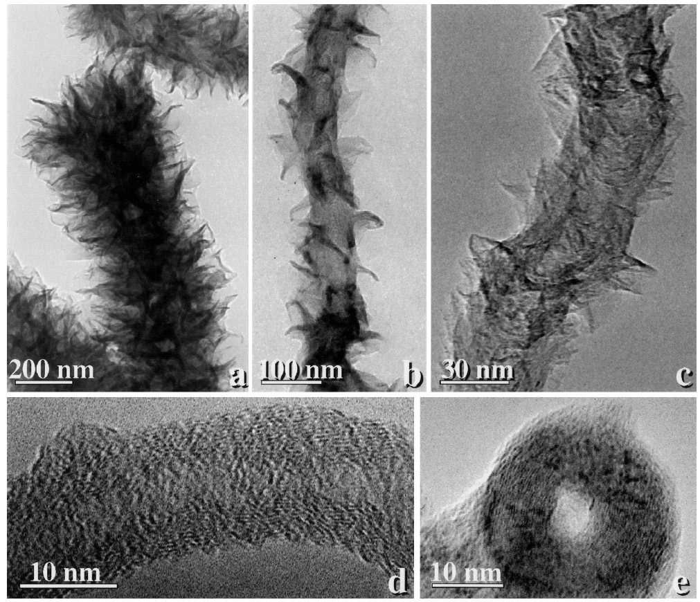
TEM investigations were performed to study the microstructure of decorated nanotubes in more detail. Figure 5 shows typical micrographs of such C-N nanotubes with decreasing outer diameter obtained at increasing . The same tendency as given in Fig. 4 was confirmed by TEM analysis. Furthermore Figs. 5(a-c) reveal again structures radiating from the surface of the nanotubes. High resolution TEM images suggest that the needle-like structures are in fact thin bent or rolled up graphene sheets.
In the case of thick nanotubes the inner structure is difficult to study due to the decoration that reduces the electron transparency. The contrast in Figs. 5(d-e) clearly represents the tubular structure of very thin C-N nanotubes and suggests that they are probably hollow inside. Tubes aligned parallel to the electron axis (Fig. 5(e)) indicate concentric wall structures and an inner diameter in that case of less than 5 nm. The two high magnification micrographs of individual tubes in plan view (Fig. 5(d)) and cross section (Fig. 5(e)) reveal the occurrence of a crystalline structure. The lattice fringes visible in Figs. 5(d,e) correspond to the {002} basal planes of graphite. Locally the planes are roughly parallel to each other but on a larger scale they show bending and interlinking between planes. Such a buckling effect of the basal planes reflecting the disorder even on atomic scale has been also observed in previously reported CNx structures 14 ; 17 ; 18 but also in pure carbon nanotubes catalytically grown 35 .
Raman spectroscopy
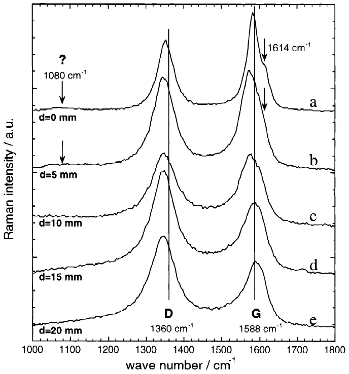
The influence of the local substrate temperature Tsub during deposition of the various types of C-N tubular structures was investigated by Raman spectroscopy. The bonding states in carbon based materials depend on the nature of polymorphs, which is influenced by the deposition parameter. These effects are illustrated in Fig. 6, which compares the micro-Raman spectra generated from nanotubes grown at different lateral distances d increasing from 0 to 20 mm as indicated.
All spectra were decomposed into at least two strong peaks confirming the graphitic-like structure of the material. It is known that pyrolythic graphite leads to a sharp vibration mode at 1588 cm-1 36 due to the presence of C-sp2 domains (first order G band). Structural modifications result in a shift of this peak to lower wave numbers as seen in curves (a-c). A shift to higher wave numbers, i.e. higher activation energy of the vibration mode, as seen in curve (e) might be caused by internal stress in the material. A second strong peak at approximately 1360 cm-1 is considered to represent a more disordered structure labelled as D (disordered) band 37 . Decreasing particle size, bending of the lattice fringes as well as incorporation of N into the structure may activate this band and cause furthermore the observed peak-shifts. Note that in a perfect graphitic crystal this first order vibrational mode is forbidden due to the selection rules.
Analysing the G band in more detail, a shoulder located at approximately 1614 cm-1 becomes clearly visible (marked by an arrow in Fig. 6). This additional vibration mode appears at high Tsub, i.e. between 0 and 4 mm and it is less pronounced below 750∘C. Beside that, a significant shift of the measured G peak position was observed as a function of . The largest deviation = 15 cm-1 was detected at = 5 mm (curve b) corresponding to decorated C-N nanotubes with an outer diameter less than 50 nm.
It is worth studying the relative Raman peak area intensities of the D and G band (ID/IG). It was found that the ID/IG peak ratio increases from 0.5 for spectrum (a) to 2.5 (spectrum e). This behaviour can visibly verified in Fig. 6 since the D band becomes dominant for large . In line with the discussion above, the D band arises from the finite size of the graphite domains and originates from grain boundaries or imperfections, such as substitutional N atoms, sp3 carbon, or other impurities 38 . Therefore the relative Raman peak area intensities of the D and G band are a measure of the degree of order of graphite clusters in the C-N tubes, which decreases with increasing . According to 39 one can estimate the length of the graphite cluster from the ID/IG ratio using the following equation: nm . In the case of our decorated C-N nanotubes, graphite cluster sizes of approximately 9 and 2 nm, respectively, were obtained for = 0 and 20 mm.
The half width of the peaks varies only slightly in the presented curves and reflects either the degree of crystalline perfection in the case of sharp peaks or the more amorphous-like character of the material (broader overlapping peaks as in curve (e)). An additional band located at approximately 1080 cm-1 was detected at the tubular structures deposited at small lateral distances but it could not yet identified.
Field emission
Field emission is one of the most promising applications for carbon-based films, and recent studies have stressed the determinant influence of the film morphology on the emission properties 10 ; 40 ; 41 ; 42 ; 43 . The ability to tailor the tube diameter by HF-CVD could thus prove to be a decisive advantage to produce emitting structures of high quality.
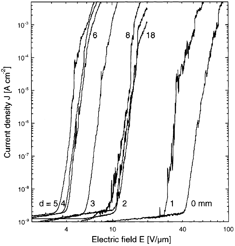
The effect of the distance to the filament, and hence of the tube diameter, is displayed in Fig. 7. The field emission was measured at 20 locations on the film between = 0 and 20 mm as indicated, and Fig. 7 shows clearly a strong variation in the field emission properties. Directly underneath the filament ( = 1 mm), no field emission below 1100 V applied voltage (which corresponds to the limit of our acquisition setup) was observed unless the interelectrode distance was decreased to 10 m. The onset field (applied field necessary to obtain a current density of 10 nA cm-2) was 36 V/m, and the threshold current density of 10 mA cm-2 was not obtained below 95 V/m. As increased, the fields decreased rapidly (see Fig. 7), and reached a minimum for = 5 mm. The interelectrode distance was 125 m at that point, and the onset and threshold fields were 3.7 and 7.2 V/m, respectively. Beyond that distance, the emission fields increased again, and levelled off for distances larger than = 8 mm. In that region, the interelectrode distance was 50 m, and the onset and threshold fields amounted to 10 and 20 V/m, respectively.
Field emission results are usually analysed with Fowler-Nordheim theory. The Fowler-Nordheim model describes the electron emission from a flat surface under a high applied field by tunnelling through the triangular surface potential barrier. The emitted current, , is proportional to , where is the applied field just above the emitting surface, is the workfunction and is a constant ( V eV3/2 m-1) 44 . In the case of sharp point emitters such as the ones considered here, is generally not known and is therefore usually taken as , with the applied voltage, the interelectrode distance and the macroscopic applied field. The field amplification factor is determined solely by the geometrical shape of the emitter 45 .
In the case of Fig. 7, all emission curves followed the Fowler-Nordheim model at low emitted currents (up to 10 A cm-2), and the field amplification factor could thus be easily determined by fitting the emission characteristics with the Fowler-Nordheim formula, using a workfunction of = 5 eV 46 . The field amplification factor follows a behaviour which is reciprocal to that of the emission fields: the field amplification is very low just below the filament ( = 80 at = 0 mm). It increases rapidly with the distance and reaches a maximal value of = 750 for the most efficient tubes, and decreases then again to 300 far away from the filament.
Discussions and Conclusions
The fact that all our C-N nanotubes prepared by HF-CVD are always decorated may probably interpreted by at least two simultaneous growth mechanisms. The results allow one to suppose a tubular growth (along the tube axis) on the one hand and the formation of graphitic foils on the other hand. In the later case one can assume as a hypothesis that small flake-like aggregates are already formed in the plasma close to the filament and are attached to the outer surface of the tubes, where they can act as nuclei for a growth of the needle-like graphene sheets. The observed splitting of the Raman G peak at high Tsub may probably also originated by one more ordered and another disordered graphitic-like structure corresponding to the two different growth mechanisms.
In the temperature range from Tsub = 700 to 820∘C a continuous increase of the tube diameter (50-1000 nm) with temperature was observed. This strong correlation seems to be a behaviour of universal character due to its independence on the major deposition parameter such as catalyst, kind and concentration of hydrocarbon gases, Tfil, , bias potential and working pressure (over large ranges).
Since several years pure carbon fibres have been grown from the decomposition of hydrocarbons (e.g. methane, acetylene, benzene, natural gas) at lower temperatures (e.g. 300∘C - 700∘C) in the presence of a metallic catalyst (e.g. Fe, Ni, Co) 47 . The diameter of such carbon filaments range from several hundred micrometers to about 100 nm and decreases with increasing temperature. Sporadic works also showed synthesis of hollow tubes in this temperature region 48 . Moreover thermal decomposition of acetylene in an oven at temperatures above 720∘C results as well in catalytic growth of nanotubes whose diameter increases with temperature 49 . However, carbon based nanotubes seem to exhibit minimum diameter in the temperature range from 720 to 750∘C confirmed by the present work.
The dispersion of the tube diameters above 7 mm may be attributed to nonequilibrium growth conditions in this region far from the filament. Due to the small deposition rate an effect of various nucleation times and an influence of a flux gradient should probably considered here as well.
The field emission properties (turn-on fields, field amplification) were clearly correlated to the diameter of the tubular C-N structures. The minimal fields and highest amplifications were found around = 4 - 6 mm, i.e., where the lowest overall values for the tube diameter are obtained (50 nm). Field emission is a highly selective process, and only structures showing the highest field amplification (e.g., the smallest tube diameter) will participate in a significant proportion to the electron emission. The fact that the emission is not as efficient for larger diameters shows however that the field emission is not governed solely by the diameter of the smallest tubes. In fact, if this were the case the emission fields should decrease further for larger , as the diameter of the smaller species decreases further to 30 nm far away from the filament. One observes however on the SEM micrographs (e.g., Fig. 3(d)) that the smaller tubes are surrounded by thicker and higher tubular structures. In such a case, the field amplification is not only determined by the diameter, but also by the distance to the neighbouring tubes 42 ; 43 ; 50 . The field amplification on a film is therefore influenced both by the geometrical shape of the emitter and by its surroundings, as the presence of nearby objects may screen the applied electric field and provoke a decrease in the effective field amplification.
The C-N nanotubes obtained by HF-CVD compare quite well with pure carbon nanotubes obtained by the catalytic decomposition of acetylene in a tube flow reactor at 720∘C 43 . The latter samples were also structured by microcontact printing using catalyst Fe:Ni inks of different densities with patterns identical to the ones used here. The best nanotube sample had onset and threshold fields of 1.8 and 3.3 V/m, with a field amplification of = 1208. Carbon nanotube films with slightly inferior properties, e.g, a film prepared with an ink of lower density (resulting in less dense nanotube patterns), showed properties nearly identical to the best C-N nanotubes observed here. Actually, one carbon nanotube film had onset and threshold fields of 3.6 and 7.0 V/m for a field amplification of 850, to be compared with 3.7 and 7.2 V/m and = 750. It is hence very probable that the factors governing the field emission are very similar for the pure carbon and C-N nanotubes, and that the incorporated nitrogen plays very little, if any, role in the field emission.
Finally, we can also compare the patterned C-N tubes with continuous films obtained by the same method 33 . The best emission obtained on a continuous film was characterised by onset and threshold fields of 3.8 and 7.8 V/m and a = 675, i.e. slightly inferior to the structured sample at = 5 mm. The continuous films show however poor homogeneity, and the structured deposition of the catalyst allows a far better control over the emission properties of the sample.
Due to the single filament configuration a strong temperature gradient appears, which give rise to the observed variations in tube diameter. The most promising range for application regarding to the field emission properties was found to be at = 4 - 6 mm corresponding to Tsub = 720-760∘C. However, once the optimal conditions have been determined, homogeneous and controlled film growth can be obtained by adjusting and Tfil in a multiple parallel filament arrangement as described recently 34 .
Acknowledgements
The Swiss National Science Foundation (SNSF) is acknowledged for the financial support. The electron microscopy was performed at the Centre Interdepartmental de Microscopie Electronique of EPFL. The authors are grateful to Yann von Kaenel from Departement des Materiaux of EPFL for technical assistance in Raman spectroscopy and to Laszlo Forro from Department de Physique of EPFL for fruitful discussions.
References
- (1) Kroto HW, Heath JR, O Brian SC, Curl RF, Smalley RE, C60: Buckminsterfullerene. Nature 1985;381(6042):162-3.
- (2) Iijima S. Helical microtubules of graphitic carbon. Nature 1991;354(6348):56-8.
- (3) Ugarte D, Curling and closure of graphitic networks under electron-beam irradiation. Nature 1992;359(6397):707-9.
- (4) Iijima S, Yudasaka M, Yamada R, Bandow S, Suenaga K, Kokai F, Takahashi K, Nano-aggregates of single-walled graphitic carbon nano-horns. Chem Phys Lett 1999;309(3-4):165-70.
- (5) Ajayan PM, Nugent JM, Siegel RW, Wei B, Kohler-Redlich Ph, Growth of carbon micro-trees. Nature 2000;404:243.
- (6) Odom TW, Huang JL, Kim P, Lieber CM, Atomic structure and electronic properties of single-walled carbon nanotubes. Nature 1998;391(6662):62-4.
- (7) Wildoer JWG, Venema LC, Rinzler AG, Smalley RE, Dekker C, Electronic structure of atomically resolved carbon nanotubes. Nature 1998;391(6662):59-62.
- (8) Yu MF, Lourie O, Dyer MJ, Moloni K, Kelly TF, Ruoff RS, Strength and breaking mechanism of multiwalled carbon nanotubes under tensile load. Science 2000;287(5453):637-40.
- (9) Salvetat JP, A.J. Kulik, J.-M. Bonard, G. Andrew, D. Briggs, T. Stockli, K. Metenier, S. Bonnamy, F. Beguin, N.A. Burnham, L. Forro, Elastic modulus of ordered and disordered multiwalled carbon nanotubes. Adv Mater 1999;11(2):161-5.
- (10) Bonard JM, Salvetat JP, Stockli T, Forro L, Kern K, Chatelain A, Field emission from carbon nanotubes: perspectives for applications and clues to the emission mechanism. Appl Phys A 1999;69(3):245-54.
- (11) Liu C, Fan YY, Liu M, Cong HT, Cheng HM, Dresselhaus MS, Hydrogen storage in single-walled carbon nanotubes at room temperature. Science 1999;286:1127-1129.
- (12) Kaltofen R, Sebald T, Weise G, Low-energy ion bombardment effects in reactive RF magnetron sputtering of carbon nitride films. Thin Solid Films 1997;308-309:11825.
- (13) Sjostrom H, Stafstrom S, Boman M, Sundgren JE, Superhard and elastic carbon nitride thin films having fullerene-like microstructure. Phys Rev Lett 1995;75(7):1136-9.
- (14) Hellgren N, Johansson MP, Broitman E, Hultman L, Sundgren JE. Role of nitrogen in the formation of hard and elastic CNx thin films by reactive magnetron sputtering. Phys Rev B 1999;59(7):5162-9.
- (15) Blase X, Charlier JC, De Vita A, Car R, Frustration effects and microscopic growth mechanisms for BN nanotubes. Appl Phys Lett 1997;70(8):197-9.
- (16) Miyamoto Y, Cohen ML, Loui SG. Theoretical investigation of graphitic carbon nitride and possible tubule forms. Solid State Communications 1997;102(8):605-8.
- (17) Suenaga K, Yudasaka M, Colliex C, Iijima S, Radially modulated nitrogen distribution in CNx nanotubular structures prepared by CVD using Ni phthalocyanine. Chem Phys Lett 2000;316(5-6):365-372.
- (18) Suenaga K, Johansson MP, Hellgren N, Broitman E, Wallenberg LR, Colliex C, Sundgren JE, Hultman L, Carbon nitride nanotubulite - densely-packed and well aligned tubular nanostructures. Chem Phys Lett 1999;300(5-6):695-700.
- (19) Stephan O, Ajayan PM, Colliex C, Redlich Ph, Lambert JM, Bernier P, Lefin P, Doping graphitic and carbon nanotube structures with boron and nitrogen. Science 1994;266(5191):1683-5.
- (20) Yudasaka M, Kikuchi R, Ohki Y, Yoshimura S, Nitrogen-containing carbon nanotube growth from Ni phthalocyanine by chemical vapor deposition. Carbon 1997;35(2):195-201.
- (21) Terrones M, Grobert N, Zhang JP, Terrones H, Olivares J, Hsu WK, Hare JP, Cheetham AK, Kroto HW, Walton DRM, Preparation of aligned carbon nanotubes catalysed by laser-etched cobalt thin films. Chem Phys Lett 1998;285(5-6):299-305.
- (22) Satishkumar BC, Govindaraj A, Sen R, Rao CNR, Single-walled nanotubes by the pyrolysis of acetylene-organometallic mixtures. Chem Phys Lett 1998;293(12):47-52.
- (23) Goldberg D, Bando Y, Bourgeois L, Kurashima K, Sato T, Large-scale synthesis and HRTEM analysis of single-walled B- and N-doped nanotube bundles. Carbon 2000;38:2017-27.
- (24) Loiseau A, Willaime F, Demoncy N, Shramchenko N, Hug G, Colliex C, Pascard H, Boron nitride nanotubes. Carbon 1998:36(5-6):743-52.
- (25) Redlich Ph, Loeffler J, Ajayan PM, Bill J, Aldinger F, Ruhle M, B-C-N nanotubes and boron doping of carbon nanotubes. Chem Phys Lett 1996;260(34):465-70.
- (26) Terrones M, Benito AM, Manteca-Diego C, Hsu WK, Osman OI, Hare JP, Reid DG, Terrones H, Cheetham AK, Prassides K, Kroto HW, Walton DRM, Metal particle catalysed production of nanoscale BN structures. Chem Phys Lett 1996;257(5-6):576-73.
- (27) Hernandez E, Goze C, Bernier P, Rubio A, Elastic properties of C and BxCyMz composite nanotubes. Phys Rev Lett 1998;80(20):4502-5.
- (28) Kurt R, Karimi A, Hoffmann V, Growth of decorated carbon nanotubes. Chem Phys Lett 2000; in print.
- (29) Kurt R, Karimi A, Influence of nitrogen on growth mechanism of decorated C-N nanotubes. Adv. Mater. 2000 in print.
- (30) Lowther JE, Defective and amorphous structure of carbon nitride. Phys Rev B 1998;57(10):5724-7.
- (31) Kind H, Bonard JM, Emmenegger C, Nilsson LO, Hernadi K, Maillard-Schaller E, Schlapbach L, Forro L, Kern K, Patterned films of nanotubes using microcontact printing of catalysts. Adv Mater 1999;11(15):1285-9.
- (32) Kind H, Bonard JM, Forro L, Kern K. Hernadi K, Nilson LO, Schlapbach L, Printing Gel-like Catalysts for the Directed Growth of Multiwall Carbon Nanotubes. Langmuir 2000; 16:6877-6883.
- (33) Kurt R, Bonard JM, Karimi A, Nano-structured nitrogenated carbon films - morphology and field emission. Diamond and Related Materials 2000; in print.
- (34) Kurt R, Bonard JM, Karimi A, Morphology and field emission properties of nano-structured nirogenated carbon films produced by plasma enhanced hot filament CVD. Carbon 2000; in print.
- (35) Hernadi K, Piedigrosso P, Fonseca A, Nagy JB, Kiricsi I, Carbon nanotube formation over supported catalysts. Molecular Crystals and Liquid Crystals 1998;310:179-84.
- (36) Tuinstra F, Koenig JL, Raman Spectrum of Graphite. The Journal of Chemical Physics 1970;53(3):1126-1130.
- (37) Dillon RO, Woollam JA, Katkanant V, Use of Raman scattering to investigate disorder and crystallite formation in as-deposited and annealed carbon films. Phys Rev B 1984;29(6):3482-3489.
- (38) Kaufman JH, Metin S, Saperstein DD, Symmetry breaking in nitrogen-doped amorphous carbon: Infrared observation of the Raman-active G and D bands. Phys Rev B 1989;39():13053-60.
- (39) Knight DS, White WB, Characterization of diamond films by Raman spectroscopy. J Mater Res 1989;4(2):385-93.
- (40) Davidov DN, Sattari PA, AlMawlawi D, Osika A, Haslett TL, Moskovits M, Field emitters based on porous aluminum oxide templates. J Appl Phys 1999; 86:3983-7.
- (41) Bonard JM, Kind H, Stockli T, Nilsson LO, Field emission from carbon nanotubes: the first five years. Sol. St. Elec. 2000; in print.
- (42) Nilsson L, Groning O, Emmenegger C, Kuttel O, Schaller E, Schlapbach L, Kind H, Bonard JM, Kern K, Scanning field emission from structured carbon nanotube films. Appl Phys Lett 2000;76:2071-2073.
- (43) Bonard JM, Weiss N, Kind H, Stockli T, Forro L, Kern K, Chatelain A, Tuning the field emission properties of patterned carbon nanotube films, Adv Mater 2000; in press.
- (44) Gadzuk JW, Plummer EW. Field emission energy distribution (FEED). Reviews of Modern Physics 1973;45(3):487-548.
- (45) Dyke WP, Dolan WW, Field Emission. In: Marton L, editor. Advances in Electronics and Electron Physics, vol 8, New York: Academic, 1956:89-185.
- (46) Dean KA, Groening O, Kuttel OM, Schlapbach L, Nanotube electronic states observed with thermal field emission electron spectroscopy. Appl Phys Lett 1999;75(18):2773-5.
- (47) Dresselhaus MS, Dresselhaus G, Eklund PC, Science of Fullerenes and Carbon Nanotubes. Academic: San Diego.1996.
- (48) Ivanov V, Fonseca A, Nagy JB, Lucas A, Lambin P, Bernaerts D, Zhang XB, Catalytic production and purification of nanotubules having fullerene-scale diameters. Carbon 1995;33:1727-35.
- (49) Klinke C, Bonard JM, Kurt R, Kern K, Temperature dependence of the growth of patterned nanotube films. under preparation.
- (50) Groning O, Kuttel OM, Emmenegger C, Groning P, Schlapbach L, Field emission properties of carbon nanotubes. J Vac Sci Technol B 2000;18(2):665-78.