Quantum Junction Plasmons in Graphene Dimers
Abstract
The interaction between doped graphene nanoislands connected by narrow junctions constitutes an ideal testbed to probe quantum effects in plasmonic systems. Here, the interaction between graphene plasmons in neighboring nanoislands is predicted to be extremely sensitive to the size and shape of the junctions. The reported ab initio calculations reveal three different regimes of interaction: (1) for narrow bridges ( carbon-atom rows), the conductance of the junction is too low to allow electron transport and the optical response is dominated by a characteristic bonding dipolar dimer mode that also appears in a classical description; (2) for wider junctions (4-8 carbon rows), a strong charge polarization is induced across the junction, which gives rise to a novel junction plasmon that has no counterpart in a classical description; (3) for even wider junctions ( rows), their conductance is sufficiently large to allow charge transport between the two graphene islands, resulting in a pronounced charge-transfer plasmon, which can also be described classically. This work opens a new path for the investigation of intrinsic plasmon quantum effects.
I Introduction
A major advantage of plasmons –the collective excitations of conduction electrons in metals– is that they can produce high levels of light confinement and optical field enhancement Li et al. (2003), which enable them to strongly interact with objects that have relatively low optical cross-sections, such as atoms and simple molecules in solid-state environments Álvarez-Puebla et al. (2010). Additionally, confined plasmons can display intense dipoles through which they couple to external radiation. Therefore, plasmons can act as intermediaries (antennas) that boost the interaction of light with molecules (e.g., in techniques as useful as surface-enhance Raman scattering (SERS) Kneipp et al. (1997); Xu et al. (1999) and surface-enhanced infrared resonant absorption (SEIRA) Kundu et al. (2008), and also in promising applications to tumor removal O’Neal et al. (2004), drug delivery Luo et al. (2011), improved photovoltaics Atwater and Polman (2010), and catalysis Jain et al. (2008)). An interesting scenario is found when a plasmon is supported by a single molecular structure rather than an extended nanoparticle. Many molecules have been found to exhibit plasmons Kociak et al. (2000); Stéphan et al. (2002); Yan et al. (2007); Yan and Gao (2008); Zhou et al. (2012), including the C60 molecule and carbon nanotubes Saito et al. (1991); Keller and Coplan (1992). Like other carbon allotropes, they display plasmon bands at energies around eV ( plasmons) and eV ( plasmons). However, these are conventional plasmons, in the sense that they are not too sensitive to the charge state of the molecules, similar to those found in noble metal nanoparticles. Instead, we are here concerned with plasmons hosted by doped graphene molecular nanostructures, which in contrast to noble-metal plasmons, only occur when they are electrically charged. These plasmons emerge at lower energies for typical levels of doping.
Graphene has recently emerged as an attractive electrically tunable, optical material Li et al. (2008) displaying strong infrared plasmons, the frequencies of which scale roughly as with the doping charge density Wunsch et al. (2006); Hwang and Das Sarma (2007); Hill et al. (2009); Jablan et al. (2009). Graphene plasmons provide unprecedented levels of light confinement and field enhancement Koppens et al. (2011), which are promising tools for accessing quantum-optics phenomena Chang et al. (2006); Dzsotjan et al. (2010); Savasta et al. (2010); Manjavacas et al. (2011). In this context, graphene offers the additional benefits of a robust structure and a simple and convenient electrical tunability for controlling quantum interactions Manjavacas et al. (2012). The electrical modulation of graphene-plasmon-related phenomena also suggests potential application in optical waveguiding and signal processing Vakil and Engheta (2011); Nikitin et al. (2011); Christensen et al. (2012), metamaterials Thongrattanasiri et al. (2012a); Nikolaenko et al. (2012), quantum optics Koppens et al. (2011), and spectrometry Ju et al. (2011). Experimental evidence of electrostatic control over plasmonic features in the absorption spectra of graphene has been recently reported Ju et al. (2011), followed by the observation and spatial mapping of confined plasmons in this material Chen et al. (2012); Fei et al. (2012). Additionaly, graphene has been used to extrinsically modulate the plasmons of neighboring metallic structures Emani et al. (2012); Grigorenko et al. (2012). These advances have sparked considerable interest into the unique optical behavior of nanostructured graphene.
Here, we describe intrinsic quantum effects in the plasmonic response of bowtie graphene nanodimers bridged by thin junctions. Due to the two-dimensional character of this material, the addition of a small number of atoms () is sufficient to dramatically modify the absorption spectrum of the entire dimer. Three distinct regimes of plasmonic behavior are predicted by our first-principles calculations. For separated nanotriangles bridged by narrow junctions ( atomic rows wide), we find a characteristic hybridized bonding dipolar plasmon (BDP) mode Nordlander et al. (2004). In the limit of wide junctions (more than 8 atomic rows), a dramatic reshaping of the optical spectrum leads to a pronounced charge-transfer plasmon (CTP), which emerges at lower energies, similar to what happens when the gap vanishes in a conventional metallic nanoparticle dimer Romero et al. (2006); Lassiter et al. (2008); Zuloaga et al. (2009); Esteban et al. (2012). The plasmonic features in both of these regimes are also found within a classical electrodynamics description using the appropriate dielectric permittivity for the graphene, although the behavior of the CTP is substantially modified by quantum mechanical effects (see below). In contrast, for intermediate junction widths ( atomic rows), a plasmonic feature shows up at intermediate energies, which is absent in classical-electrodynamics calculations. We refer to this mode as a junction plasmon (JP) because it is caused by quantum effects in the small molecular junction. We also predict a minor dependence on the length of the junction and a strong dependence on its width, thus confirming the importance of a quantum mechanical description of the optical properties of bridged graphene dimers.
II Results and discussion
We simulate the optical response of nanoscale bowtie graphene structures using the random-phase approximation (RPA) and wave functions derived from a tight-binding description of the carbon sheet. Further details of the method are given elsewhere Thongrattanasiri et al. (2012b). The triangular structures forming the bowties are oriented with respect to the graphene lattice in such a way that they have armchair edges, which prevent undesired losses typically observed in zigzag-edge structures, and caused by the presence of zero-energy electronic edge states Thongrattanasiri et al. (2012b). Such states are not present in the structures under consideration, because they have the same number of atoms in both carbon sublattices Fernández-Rossier and Palacios (2007). For comparison, we include classical-electrodynamics calculations, which are performed by describing the graphene through its local-RPA surface conductivity Koppens et al. (2011) using a finite elements method (COMSOL). We fix the side length of the nanotriangles to 8 nm in all cases ( atoms in each triangle). We set the Fermi energy of our structures to eV, and the intrinsic damping to meV, corresponding to a DC mobility of 10,000 cmVs Jablan et al. (2009).
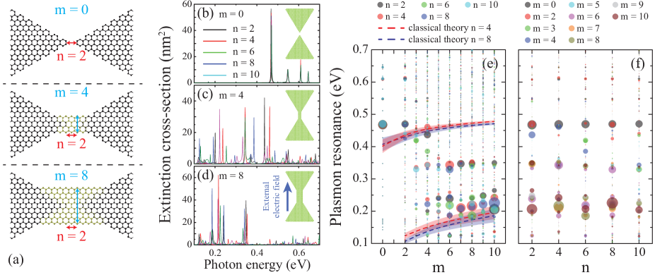
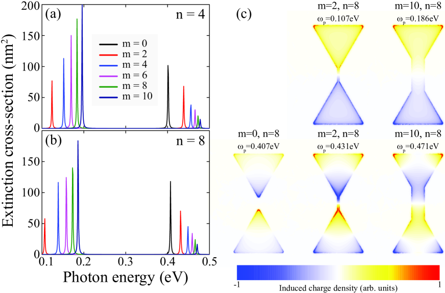
Our main results are summarized in Fig. 1. We show details of the junction region in Fig. 1(a) for three characteristic values of the width (, where is the number of carbon-atom zigzag rows forming the junction, and stands for the non-touching configuration). The corresponding spectra are shown in Fig. 1(b)-(d) for a range of junction lengths [ is defined as the number of carbon hexagons that are needed to join the graphene triangles for , see Fig. 1(a)]. These spectra show a clear trend from high to low energy features as the junction width is increased, irrespective of the length. This behavior is further examined in Fig. 1(e), where the plasmon features are arranged as a function of energy (vertical axis) and junction width (, horizontal axis) for different values of the junction length (see color code in the upper inset; full spectra are provided in the Appendix (Fig. 4). The area of the circles is made proportional to the intensity of the plasmon mode defined as the area under the corresponding plasmon peaks in the extinction spectra (for light polarization along the gap). For narrow bridges, the spectra exhibit prominent plasmonic features centered around eV. In contrast, the spectra for the wide-junction limit are dominated by lower-energy plasmonic features around eV. At intermediate values of the junction width, there is a complex transition between these two regimes, with intermediate-energy features around eV showing up in the spectra. The transition is fast, but not singular. These conclusions seem to be rather independent of the length of the junctions . As Fig. 1(e) illustrates, no significant spectral changes are induced when the plasmon energies are plotted as a function of junction length . The three distinct behaviors of the plasmon energies noted above for narrow, intermediate, and wide junctions appear for all values of the junction length.
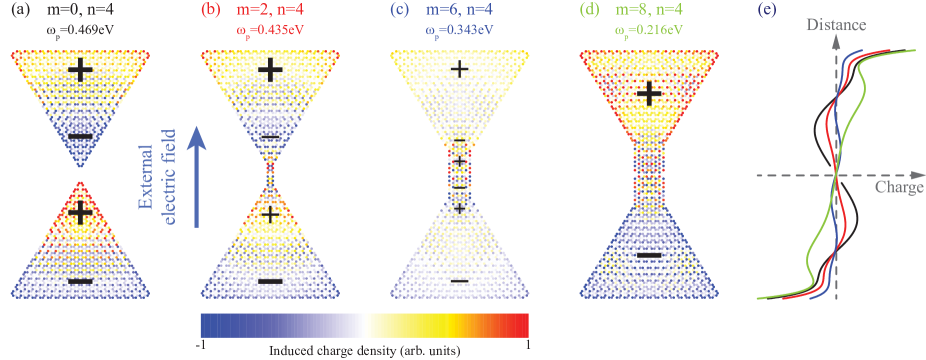
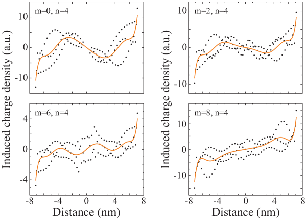
Further insight into the character of these plasmons is provided by examining their induced-charge distributions, which are plotted in Fig. 2(a)-(d) for representative structures along the transition from narrow to wide junction regimes. The polarization profile for the high-energy plasmon around eV in the non-touching dimer [, Fig. 2(a)] displays a dipole-dipole pattern that is not substantially modified when a narrow junction [, Fig. 2(b)] is present between the two triangular islands of the structure. This distinct polarization pattern is characteristic of a BDP. In contrast, the intermediate energy plasmon around eV [Fig. 1(c)] for a junction width shows a clear dipolar polarization pattern across the junction. This is the JP that is formed from the local electronic properties of the junction. A weak charge transfer between the two nanotriangles is also evident in the plot and corresponds to the CTP, which is delocalized over the entire graphene structure like an standing wave. The latter shows a consistent charge polarization that does not change with increasing , as shown for in Fig. 2(d). The CTP becomes the dominant feature once the junction is sufficiently wide. The signs superimposed on the density plots of Fig. 2(a)-(d) qualitatively correspond to the distribution of the plasmon induced charge as a function distance to the dimer center, which is shown in Fig. 2(e) (see also Fig. 6 in the Appendix). This analysis is rather independent of the length of the junction . An in-depth inspection of bowties of increasing length leads to results that are consistent with the above conclusions, including the emergence of quantum junction plasmons once the width of the junction and the length of the structure are sufficiently large (see Fig. 10 in the Appendix for more details).
A classical-electrodynamics description of these graphene nanostructures (see broken curves in Fig. 1(e) and Fig. 5 in the Appendix) does not completely reproduce the plasmonic behavior derived from first-principles. For instance, classical calculations miss the intermediate-energy junction plasmon that we observe in the quantum calculations for intermediate junction widths. Another discrepancy is that classical theory predicts a smooth fadeout of the dipole-dipole mode exhibited by non-overlapping triangles when the junction width is increased, while the CTP shows a singular behavior, as it migrates towards zero energy in the limit of vanishing junction width. This is in striking contrast to the results from the quantum description, in which the CTP is rather dispersionless and fades out smoothly in that limit [see Fig. 1(e)]. The dipole-dipole and charge-transfer nature of the classically predicted plasmons is clear from their induced-charge distributions (see Appendix, Fig. 5).
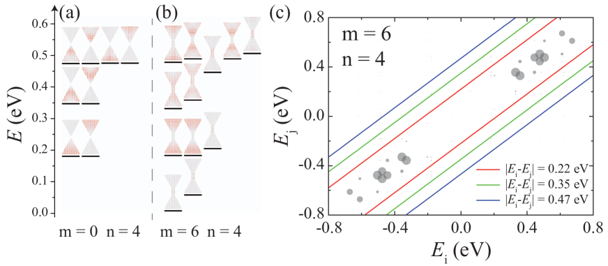
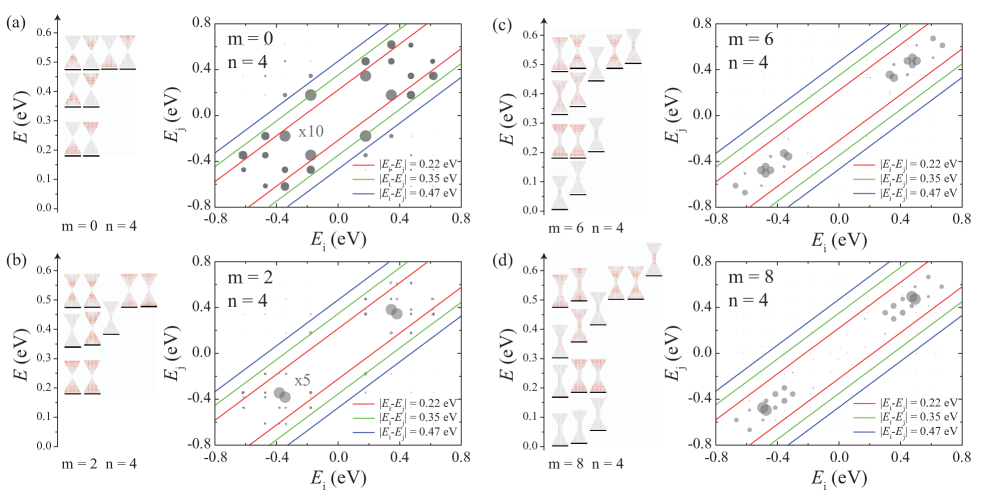
The electronic states involved in the plasmon of separated nanotriangles [Fig. 3(a)] are nearly identical to those of individual triangular islands, but with a small amount of Coulombic interaction and hybridization. When a bridge of intermediate width is added to form a junction [Fig. 3(b)], the level of hybridization of these states increases, and new electronic junction states emerge. In particular, two new junction states are observed near the Dirac point (zero energy), which are expected due to the presence of carbon zigzag edges in the bridge Akhmerov and Beenakker (2008); Wimmer et al. (2010). Thus, the junction plasmon noted above must be supported by excitations involving electrons or holes in these electronic junction states. The strength of the electron-hole pair (e-h) dipole transitions in this system are represented in Fig. 3(c) as a function of initial and final energies (the strength is represented through the area of the circles). Clearly, the plasmon energies (solid curves) do not strongly overlap with the dominant e-h transitions. This energy mismatch shows that the optical transitions are not single-particle excitations and is a strong argument supporting our conclusion of collective plasmonic nature of the bowtie optical excitations under consideration. Similar results are observed for different widths of the junction (see Appendix, Fig. 9).
III Outlook and conclusions
Graphene dimers provide advantageous systems compared to metallic dimers both because of the structural robustness of this material and because the carbon structure can be reliably imaged with atomic detail Ç. Ö. Girit et al. (2009); Subramaniam et al. (2012), and therefore, a detailed correlation between atomic structure and optical response is within reach experimentally. This is not the case of gaps formed by closely spaced three-dimentional metallic particles or tips Koh et al. (2009); Yamamoto et al. (2011), which suffer from inherent faceting and structural uncertainties. Planar graphene nanostructures are thus ideal systems on which to study the interplay between structural features (e.g., ripples and defects) and the plasmonic response (for example, the amount by which they increase the plasmon scattering and dephasing rate via electron-hole pair generation). Recent advances in atomically resolved imaging Tian et al. (2011) and patterning Börrnert et al. (2012) of graphene should facilitate this task.
The remarkably large variations here reported in the optical properties of plasmonic structures consisting of thousands of carbon atoms by just adding a few () extra atoms provides a handle for tuning plasmons in graphene. Together with the already established chemical Wehling et al. (2008) and electrical Novoselov et al. (2004) tunability of this material, this adds a novel tuning parameter, which can be potentially exploited for ultrasensitive optical sensing (e.g., by analyzing the dependence on the presence of molecules near the junction, which can modify the local valence charge density).
Although for simplicity we only discuss above free-standing graphene with a Fermi energy eV, no qualitative changes are observed for different doping or when the graphene sheet is placed on a substrate (see Appendix, Figs. 7 and 8). Quantum effects are found to be more significant when the level of doping is reduced (see results for eV in the Appendix, Figs. 7), as one expects for the smaller number of doping electrons participating in the plasmons, whereas the CTP energies are closer to the classical description when the doping increases (see eV results in the Appendix, Figs. 7).
In conclusion, using a fully quantum mechanical approach we have studied the optical properties of graphene dimers consisting of several thousand carbon atoms connected by a narrow graphene junction. The optical properties of the system are found to be strongly sensitive to the detailed structure of the junction, with the spectrum exhibiting drastic changes with the addition of a few carbon atoms in that region. In addition to the conventional hybridized and charge transfer plasmons observed for metallic dimers Romero et al. (2006); Lassiter et al. (2008); Zuloaga et al. (2009); Esteban et al. (2012), graphene dimers display junction plasmons of a purely quantum mechanical origin, which does not seem to appear in conventional metallic junctions Savage et al. (2012). The plasmonic response of this graphene structure is found to be strongly influenced by quantum effects, making it of significant interest in the emerging field of quantum plasmonics as well as for novel nanophotonics and optoelectronics applications.
ACKNOWLEDGMENT
This work has been supported in part by the Spanish MEC (MAT2010-14885 and Consolider NanoLight.es) and the European Commission (FP7-ICT-2009-4-248909-LIMA and FP7-ICT-2009-4-248855-N4E). A.M. acknowledges financial support through FPU from the Spanish MEC. P.N. acknowledges support from the Robert A. Welch Foundation under grant C-1222.
APPENDIX
In this appendix, we provide detailed results of first-principles extinction spectra, electron states, and plasmon-induced charge densities for the graphene bowtie structures under consideration. Additionally, we study the evolution of plasmons in bowties of increasing length. Classical-electrodynamics calculations are also offered for comparison.
We choose a Fermi energy eV (except in Fig. 7) and an intrinsic damping meV, corresponding to a DC mobility of 10,000 cmVs. We set the temperature to K, although thermal effects are negligible for the plasmons under consideration, the energies of which are high compared with . The external light polarization is taken along the junction between the nanotriangles forming the bowties. The triangle side-length is set to 8 nm, except in Fig. 10. Our first-principles calculations are performed following methods described elsewhere Thongrattanasiri et al. (2012b). For the classical calculations of Fig. 5 we use a finite-element method (COMSOL) following a previously reported prescription Koppens et al. (2011) according to which the graphene is treated as a thin dielectric layer.
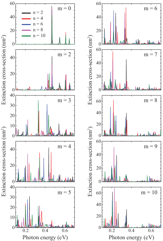
We show in Fig. 4 the full series of extinction spectra from which Figs. 1(e) and 1(f) are constructed. The cross section is given in square nanometers, so it can be directly compared with the geometrical area of the graphene in the bowties nm2. The maximum cross-section obtained in these first-principles calculations is approximately half the geometrical area. In contrast, the cross sections derived from classical electrodynamics (Fig. 5) can reach substantially large values compared with the geometrical area. The energies of the plasmons derived from classical calculations are represented in Fig. 1(e) for comparison.
The charge densities associated with the plasmons (Fig. 2) are examined in more detail in Fig. 6, where they are shown to exhibit strong modulations between nearest-neighbor carbon-atom rows. These modulations oscillate between three smoothly varying limits, as expected from the three different types of atomic sites in the armchair edges of the nanotriangles under consideration. The curves plotted in Fig. 2, and reproduced in Fig. 6 for convenience, correspond to averages over four carbon-atom neighbors.
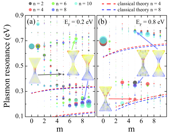
We have considered the effect of doping in Fig. 7, where we plot data similar to Fig. 1(e) (eV), but changing the doping level to eV (Fig. 7(a)) and eV (Fig. 7(b)). As a general trend, we observe a reduction in the role of quantum effects as the doping level is increased. For example, for eV we observe that charge-transfer plasmons (CTPs) pile up around eV in the quantum description, whereas classical theory places them at much lower energies; in contrast, both classical and quantum descriptions agree much better in the energies of CTPs for eV; and an intermediate situation is encountered for eV. Likewise, junction plasmons (JPs) appear to lose strength relative to the rest of the features as increases. Actually, these plasmons cover a wide spectral region extending above the energies of CTPs for eV as the junction width is varied, whereas they are only discernable in the range of junction widths for eV.
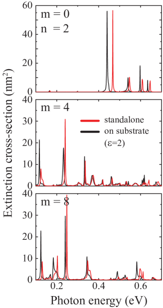
For simplicity, we present in this paper results for self-standing graphene, except in Fig. 8, where we study the effect of depositing the carbon layer on a glass substrate (). In a classical description of graphene, the net effect of the substrate is to change the conductivity to an effective value Christensen et al. (2012). This leads to a redshift of the plasmon energies by a factor . We show in Fig. 8 that a similar trend is observed in small graphene structures within our quantum-mechanical description, thus corroborating that the conclusions of our study also apply to the more physical situation of supported graphene nanostructures. The features of the extinction spectra are maintained by introducing a substrate, which essentially produces a redshift that is substantially smaller than that predicted by classical theory in our relatively small structures, particularly for the lowest-energy features and the widest junction considered in Fig. 8.
The electron wave functions and the strength of dipolar transitions connecting them are considered in Fig. 9, which is an extension of Fig. 3 including more junction widths. One can clearly observe the increasing involvement of electron junction states as the junction becomes wider.
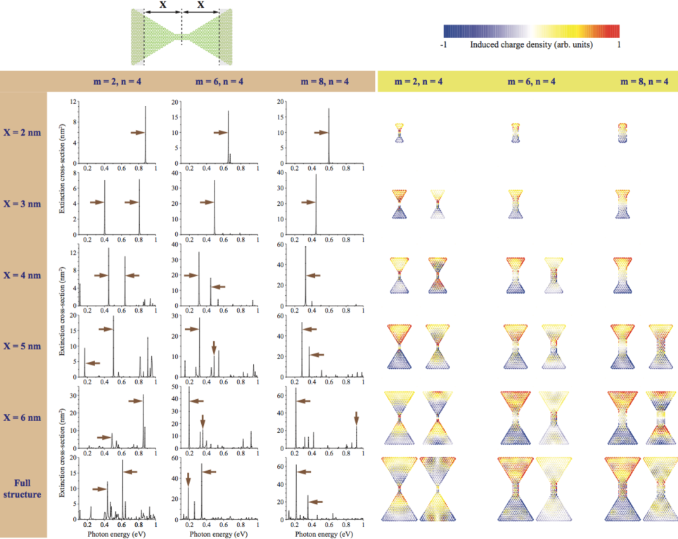
Finally, we study in Fig. 10 the evolution of plasmons in bowties as a function of the length of the structures. We fix the junction length to hexagons and consider three different junction widths consisting of , 6, and 8 carbon zigzag rows. In general, we observe a migration of modes with similar symmetry towards lower plasmon energies as the bowtie length increases. For the two shorter series under consideration (half length , 3, and 4 nm), we find a dominant CTP, with opposite induced charges in each half of the dimer. For larger bowties, higher-order modes become relevant. For example, the structure with the narrower junction () exhibits a dipole-dipole plasmon, which ends up at eV at the full length nm (lower row of Fig. 10). For this junction width, the CTP becomes relatively weak with nm, so it does not make a relevant contribution to the full structure. In contrast, the CTP remains a dominant feature for all the lengths under consideration in structures bridged by wider junctions ( and 8). As the length increases, a new dipole mode starts developing, which is associated with large charge pileup at the junction. This is the intermediate-energy feature observed in Fig. 1(e).
References
- Li et al. (2003) K. R. Li, M. I. Stockman, and D. J. Bergman, Phys. Rev. Lett. 91, 227402 (2003).
- Álvarez-Puebla et al. (2010) R. A. Álvarez-Puebla, L. M. Liz-Marzán, and F. J. García de Abajo, J. Phys. Chem. Lett. 1, 2428 (2010).
- Kneipp et al. (1997) K. Kneipp, Y. Wang, H. Kneipp, L. T. Perelman, I. Itzkan, R. R. Dasari, and M. S. Feld, Phys. Rev. Lett. 78, 1667 (1997).
- Xu et al. (1999) H. Xu, E. J. Bjerneld, M. Käll, and L. Börjesson, Phys. Rev. Lett. 83, 4357 (1999).
- Kundu et al. (2008) J. Kundu, F. Le, P. Nordlander, and N. J. Halas, Chem. Phys. Lett. 452, 115 (2008).
- O’Neal et al. (2004) D. P. O’Neal, L. R. Hirsch, N. J. Halas, J. D. Payne, and J. L. West, Cancer Lett. 209, 171 (2004).
- Luo et al. (2011) Y. L. Luo, Y. S. Shiao, and Y. F. Huang, ACS Nano 5, 7796 (2011).
- Atwater and Polman (2010) H. A. Atwater and A. Polman, Nat. Mater. 9, 205 (2010).
- Jain et al. (2008) P. K. Jain, X. H. Huang, I. H. El-Sayed, and M. A. El-Sayed, Accounts Chem. Res. 41, 578 (2008).
- Kociak et al. (2000) M. Kociak, L. Henrard, O. Stéphan, K. Suenaga, and C. Colliex, Phys. Rev. B 61, 13936 (2000).
- Stéphan et al. (2002) O. Stéphan, D. Taverna, M. Kociak, K. Suenaga, L. Henrard, and C. Colliex, Phys. Rev. B 66, 155422 (2002).
- Yan et al. (2007) J. Yan, Z. Yuan, and S. W. Gao, Phys. Rev. Lett. 98, 216602 (2007).
- Yan and Gao (2008) J. Yan and S. W. Gao, Phys. Rev. B 78, 235413 (2008).
- Zhou et al. (2012) W. Zhou, J. Lee, J. Nanda, S. T. Pantelides, S. J. Pennycook, and J. C. Idrobo, Nat. Nanotech. 7, 161 (2012).
- Saito et al. (1991) Y. Saito, H. Shinohara, and A. Ohshita, Jpn. J. Appl. Phys. Part 2-Lett. 30, L1068 (1991).
- Keller and Coplan (1992) J. W. Keller and M. A. Coplan, Chem. Phys. Lett. 193, 89 (1992).
- Li et al. (2008) Z. Q. Li, E. A. Henriksen, Z. Jian, Z. Hao, M. C. Martin, P. Kim, H. L. Stormer, and D. N. Basov, Nat. Phys. 4, 532 (2008).
- Wunsch et al. (2006) B. Wunsch, T. Stauber, F. Sols, and F. Guinea, New J. Phys. 8, 318 (2006).
- Hwang and Das Sarma (2007) E. H. Hwang and S. Das Sarma, Phys. Rev. B 75, 205418 (2007).
- Hill et al. (2009) A. Hill, S. A. Mikhailov, and K. Ziegler, Europhys. Lett. 87, 27005 (2009).
- Jablan et al. (2009) M. Jablan, H. Buljan, and M. Soljac̆ić, Phys. Rev. B 80, 245435 (2009).
- Koppens et al. (2011) F. H. L. Koppens, D. E. Chang, and F. J. García de Abajo, Nano Lett. 11, 3370 (2011).
- Chang et al. (2006) D. E. Chang, A. S. Sørensen, P. R. Hemmer, and M. D. Lukin, Phys. Rev. Lett. 97, 053002 (2006).
- Dzsotjan et al. (2010) D. Dzsotjan, A. S. Sorensen, and M. Fleischhauer, Phys. Rev. B 82, 075427 (2010).
- Savasta et al. (2010) S. Savasta, R. Saija, A. Ridolfo, O. Di Stefano, P. Denti, and F. Borghese, ACS Nano 4, 6369 (2010).
- Manjavacas et al. (2011) A. Manjavacas, F. J. García de Abajo, and P. N. Nordlander, Nano Lett. 11, 2318 (2011).
- Manjavacas et al. (2012) A. Manjavacas, P. Nordlander, and F. J. García de Abajo, ACS Nano 6, 1724 (2012).
- Vakil and Engheta (2011) A. Vakil and N. Engheta, Science 332, 1291 (2011).
- Nikitin et al. (2011) A. Y. Nikitin, F. Guinea, F. J. García-Vidal, and L. Martín-Moreno, Phys. Rev. B 84, 161407(R) (2011).
- Christensen et al. (2012) J. Christensen, A. Manjavacas, S. Thongrattanasiri, F. H. L. Koppens, and F. J. García de Abajo, ACS Nano 6, 431 (2012).
- Thongrattanasiri et al. (2012a) S. Thongrattanasiri, F. H. L. Koppens, and F. J. García de Abajo, Phys. Rev. Lett. 108, 047401 (2012a).
- Nikolaenko et al. (2012) A. E. Nikolaenko, N. Papasimakis, E. Atmatzakis, Z. Q. Luo, Z. X. Shen, F. de Angelis, S. A. B. E. di Fabrizio, and N. I. Zheludev, Appl. Phys. Lett. 100, 181109 (2012).
- Ju et al. (2011) L. Ju, B. Geng, J. Horng, C. Girit, M. Martin, Z. Hao, H. A. Bechtel, X. Liang, A. Zettl, Y. R. Shen, et al., Nat. Nanotech. 6, 630 (2011).
- Chen et al. (2012) J. Chen, M. Badioli, P. Alonso-González, S. Thongrattanasiri, F. Huth, J. Osmond, M. Spasenović, A. Centeno, A. Pesquera, P. Godignon, et al., Nature 487, 77 (2012).
- Fei et al. (2012) Z. Fei, A. S. Rodin, G. O. Andreev, W. Bao, A. S. McLeod, M. Wagner, L. M. Zhang, Z. Zhao, M. Thiemens, G. Dominguez, et al., Nature 487, 82 (2012).
- Emani et al. (2012) N. K. Emani, T.-F. Chung, X. Ni, A. V. Kildishev, Y. P. Chen, and A. Boltasseva, Nano Lett. 12, 5202 (2012).
- Grigorenko et al. (2012) A. N. Grigorenko, M. Polini, and K. S. Novoselov, Nat. Photon. 6, 749 (2012).
- Nordlander et al. (2004) P. Nordlander, C. Oubre, E. Prodan, K. Li, and M. I. Stockman, Nano Lett. 4, 899 (2004).
- Romero et al. (2006) I. Romero, J. Aizpurua, G. W. Bryant, and F. J. García de Abajo, Opt. Express 14, 9988 (2006).
- Lassiter et al. (2008) J. B. Lassiter, J. Aizpurua, L. I. Hernandez, D. W. Brandl, I. Romero, S. Lal, J. H. Hafner, P. Nordlander, and N. J. Halas, Nano Lett. 8, 1212 (2008).
- Zuloaga et al. (2009) J. Zuloaga, E. Prodan, and P. Nordlander, Nano Lett. 9, 887 (2009).
- Esteban et al. (2012) R. Esteban, A. G. Borisov, P. Nordlander, and J. Aizpurua, Nature Commun. 3, 825 (2012).
- Thongrattanasiri et al. (2012b) S. Thongrattanasiri, A. Manjavacas, and F. J. García de Abajo, ACS Nano 6, 1766 (2012b).
- Fernández-Rossier and Palacios (2007) J. Fernández-Rossier and J. J. Palacios, Phys. Rev. Lett. 99, 177204 (2007).
- Akhmerov and Beenakker (2008) A. R. Akhmerov and C. W. J. Beenakker, Phys. Rev. B 77, 085423 (2008).
- Wimmer et al. (2010) M. Wimmer, A. R. Akhmerov, and F. Guinea, Phys. Rev. B 82, 045409 (2010).
- Ç. Ö. Girit et al. (2009) Ç. Ö. Girit, J. C. Meyer, R. Erni, M. D. Rossell, C. Kisielowski, L. Yang, C.-H. Park, M. F. Crommie, M. L. Cohen, S. G. Louie, et al., Science 27, 1705 (2009).
- Subramaniam et al. (2012) D. Subramaniam, F. Libisch, Y. Li, C. Pauly, V. Geringer, R. Reiter, T. Mashoff, M. Liebmann, J. Burgdörfer, C. Busse, et al., Phys. Rev. Lett. 108, 046801 (2012).
- Koh et al. (2009) A. L. Koh, K. Bao, I. Khan, W. E. Smith, G. Kothleitner, P. Nordlander, S. A. Maier, and D. W. McComb, ACS Nano 3, 3015 (2009).
- Yamamoto et al. (2011) N. Yamamoto, S. Ohtani, and F. J. García de Abajo, Nano Lett. 11, 91 (2011).
- Tian et al. (2011) J. Tian, H. Cao, W. Wu, Q. Yu, and Y. P. Chen, Nano Lett. 11, 3663 (2011).
- Börrnert et al. (2012) F. Börrnert, L. Fu, S. Gorantla, M. Knupfer, B. Büchner, and M. H. Rümmeli, ACS Nano p. DOI: 10.1021/nn304256a (2012).
- Wehling et al. (2008) T. O. Wehling, K. S. Novoselov, S. V. Morozov, E. E. Vdovin, M. I. Katsnelson, A. K. Geim, and A. I. Lichtenstein, Nano Lett. 8, 173 (2008).
- Novoselov et al. (2004) K. S. Novoselov, A. K. Geim, S. V. Morozov, D. Jiang, Y. Zhang, S. V. Dubonos, I. V. Grigorieva, and A. A. Firsov, Science 306, 666 (2004).
- Savage et al. (2012) K. J. Savage, M. M. Hawkeye, R. Esteban, A. G. Borisov, J. Aizpurua, and J. J. Baumberg, Nature 491, 574 (2012).