Plasmons Driven by Single Electrons in Graphene Nanoislands
Abstract
Plasmons produce large confinement and enhancement of light that enable applications as varied as cancer therapy and catalysis. Adding to these appealing properties, graphene has emerged as a robust, electrically tunable material exhibiting plasmons that strongly depend on the density of doping charges. Here we show that adding a single electron to a graphene nanoisland consisting of hundreds or thousands of atoms switches on infrared plasmons that were previously absent from the uncharged structure. Remarkably, the addition of each further electron produces a dramatic frequency shift. Plasmons in these islands are shown to be tunable down to near infrared wavelengths. These phenomena are highly sensitive to carbon edges. Specifically, armchair nanotriangles display sharp plasmons that are associated with intense near-field enhancement, as well as absorption cross-sections exceeding the geometrical area occupied by the graphene. In contrast, zigzag triangles do not support these plasmons. Our conclusions rely on realistic quantum-mechanical calculations, which are in ostensible disagreement with classical electromagnetic simulations, thus revealing the quantum nature of the plasmons. This study shows a high sensitivity of graphene nanoislands to elementary charges, therefore emphasizing their great potential for novel nano-optoelectronics applications.
I Introduction
Light can efficiently excite plasmons (collective electron oscillations in matter), thus producing strong confinement of electromagnetic energy and huge enhancement of the associated electric fields. These phenomena have spurred a plethora of applications ranging from ultrasensitive detection Nie and Emory (1997); Kneipp et al. (1997); Johansson et al. (2005); Talley et al. (2005); Rodríguez-Lorenzo et al. (2009) to cancer therapy Qian et al. (2008); Hirsch et al. (2003) and catalysis Asahi et al. (2001); Kamat (2002), which have been largely fueled by progress in the synthesis of noble-metal nanoparticles with increasing control over size and morphology Grzelczak et al. (2008). Plasmons in conventional metals result from the cooperative effect of many electron-hole (e-h) virtual excitations around the Fermi level. The resulting plasmon frequencies scale with the power of the density of valence electrons. Understandably, massive amounts of charging are required to produce sizable frequency shifts in the plasmons Chapman and Mulvaney (2001); Hirakawa and Kamat (2004), and therefore, their electrical control remains elusive.
This scenario has substantially changed with the arrival of graphene. Plasmons exist in this material when it is doped, but now the plasmon frequency is proportional to the power of the doping charge density rather than the square root of the valence electron density Castro Neto et al. (2009). This behavior is a consequence of the peculiar electronic structure of graphene, characterized by a vanishing density of electron states at the Fermi level. Evidence for graphene plasmons has been recently reported through terahertz Ju et al. (2011) and infrared (IR) Fei et al. (2011); Yan et al. (2012a, b) optical spectroscopies, as well as through direct near-field spatial imaging Chen et al. (2012); Fei et al. (2012). These studies have conclusively demonstrated that graphene plasmons can be frequency-tuned using conventional electric gating technology. In a parallel promising effort, the electro-optical tunability of graphene has also been used to modulate the plasmonic response of neighboring metallic nanoparticles Emani et al. (2012); Fang et al. (2012a, b). Now, the question arises, is the singular electronic structure of extended graphene permeating the optical properties of nanometer-sized doped graphene islands as well? Can we bring the level of doping needed to sustain plasmons in a small structure down to just a single electron?
Here we predict that IR and near-IR (NIR) plasmons in graphene nanoislands can be switched on and off by the addition or removal of a single electron. This is a remarkable property considering that the islands contain hundreds of atoms. Specifically, we focus on graphene nanotriangles, which we describe using a combination of a tight-binding model for the electronic structure and the random-phase approximation (RPA) Pines and Nozières (1966) for the dielectric response, as explained in Appendix A. A more detailed description of the specifics of our approach is given elsewhere Thongrattanasiri et al. (2012a), essentially extending to finite graphene islands what was previously reported for more extended systems by combining tight-binding and RPA. This effort was pioneered by Wallace Wallace (1947) in graphene and graphite, and continued through outstanding analyses by other authors Wunsch et al. (2006); Brey and Fertig (2007); Castro Neto et al. (2009).
II Results and Discussion
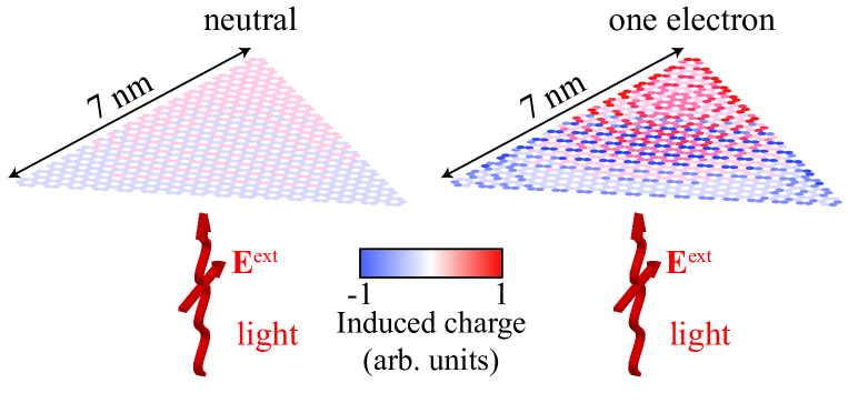
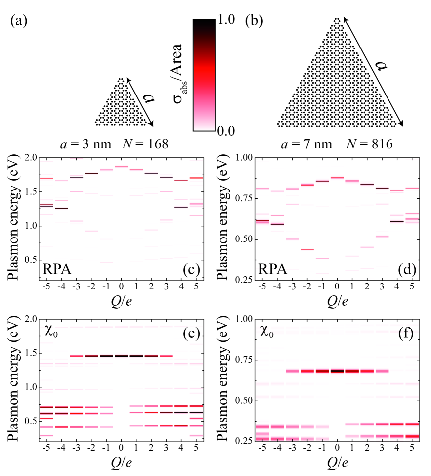
Figure 1 summarizes our main finding: an electrically neutral graphene nanotriangle (with armchair edges and 7 nm side length) does not display strong polarization when illuminated by IR light; in contrast, the addition of a single electron results in the emergence of an intense plasmon mode, so that strong polarization is produced when the light is tuned to the plasmon energy (0.38 eV). A single electron can thus trigger the existence of plasmons in the structure. When further electrons are added to such armchair nanotriangle (Fig. 2c), this IR plasmon undergoes a dramatic blue shift (in steps of eV) and it gains in strength. Notice that we denote the net charge of the structure as in Fig. 2, so that () corresponds to doping with electrons (holes).
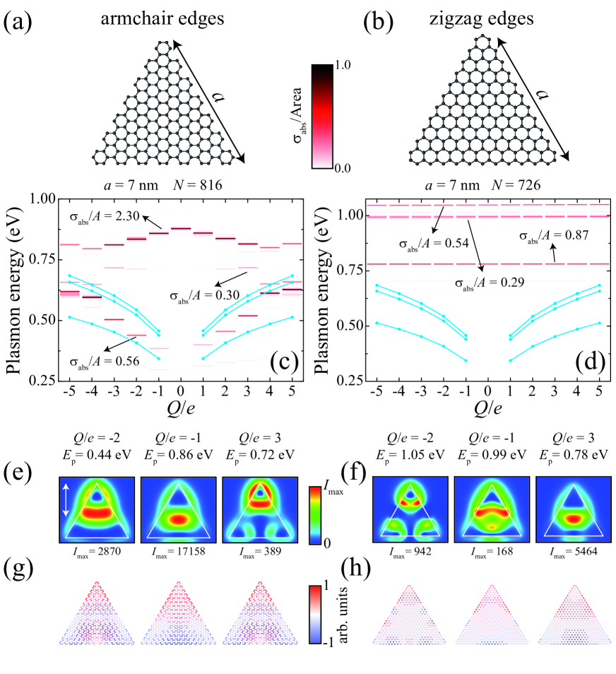
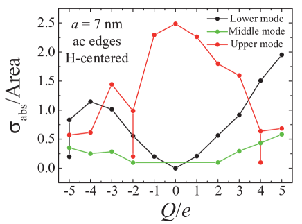
Equally important, we find a NIR plasmon with and without doping at an energy around eV. In contrast to the IR plasmon, this high-energy mode undergoes redshift with increasing doping. Both the IR and the NIR plasmons give rise to large absorption cross-sections (Fig. 2c), which can reach values exceeding the geometrical area of the graphene for large doping in the IR and for low doping in the NIR (see Appendix I).
The plasmon shift is substantially larger than the width, thus making it clearly resolvable. Obviously, this conclusion depends on the parameter used for the intrinsic width in the RPA (see Fig. 2 in Appendix A). The main contributions to the width in extended graphene originate in optical-phonon losses, impurities, and disorder. These mechanisms are well described in extended graphene Jablan et al. (2009), and we take meV (i.e., a dephasing time fs) as a reasonable estimate for high-quality samples Novoselov et al. (2004, 2005). Actually, given the small area of the islands, it should be possible to identify many of them without impurities or defects. Besides, the large shift-to-width ratios of Fig. 2 guarantee that our conclusions are still maintained with much higher losses up to the upper limit that is intuitively imposed by the lifetime of hot electrons (fs, as resolved from two-photon photoemission Armbrust et al. (2012)). Additionally, Landau-damping is expected to be negligible for low-energy plasmons in defect-free extended graphene Peres et al. (2010), and although plasmon decay into e-h pairs is made possible by the loss of translational symmetry in nanoislands, no substantial broadening is observed in the plasmons of armchair triangles beyond the intrinsic width introduced through the RPA formula (see Fig. 2 and discussion below). Actually, the plasmon energies do not overlap any intense e-h transition (see Fig. 3c below).
Incidentally, a classical electromagnetic description of the graphene (see Appendix A) also yields IR plasmons with similar shifts as the RPA calculations (Fig. 2a, blue curve), although the plasmon energies are substantially higher in the latter due to quantum confinement Thongrattanasiri et al. (2012a). However, the NIR plasmons and their redshifts with increasing doping are completely missed by classical theory.
A completely different scenario is observed in zigzag nanotriangles (Fig. 2b,d) compared to armchair structures (Fig. 2a,c): a single plasmon appears at eV instead of the IR and NIR plasmons; and the plasmon energy is rather independent of doping. This seems to be connected to the presence of near-zero-energy electronic states, which are known to exist near zigzag edges Fernández-Rossier and Palacios (2007); Ezawa (2007); Akhmerov and Beenakker (2008); Zhang et al. (2008); Wimmer et al. (2010); Zarenia et al. (2011). In a previous study Thongrattanasiri et al. (2012a), these states were found to produce plasmon dephasing in small islands. In the nanotriangle of Fig. 2b, the number of such states ( per electron spin, see Appendix F) is large enough so that the addition of extra electrons does not substantially change the electronic structure. Moreover, these states do not produce dipole transitions to higher-energy states (see Fig. 3d), and therefore, they play a dummy role in the formation of plasmons. For these reasons, mid-IR plasmons are not observed in the zigzag island, and the NIR plasmon is rather insensitive to the number of electrons added to it, until the zero-energy electronic levels are completely filled (plasmons shifts are predicted beyond this level of doping, as shown in Appendix F).
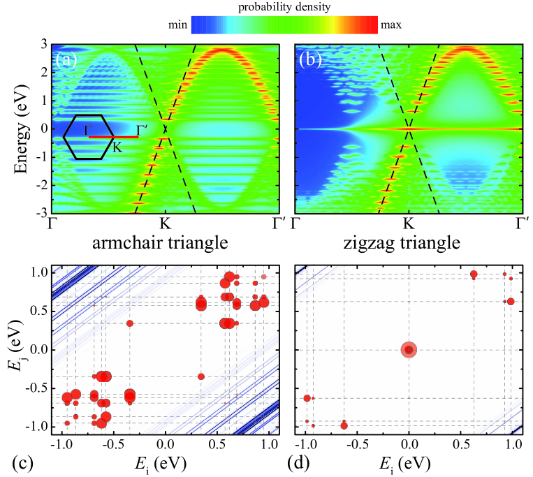
In extended graphene, the Dirac-cone band structure leads to a gap between intra- and inter-band e-h transitions. Long-lived plasmons exist in that gap. In nanoislands, the electron parallel momentum is not a good quantum number due to the lack of translational symmetry, but we can obtain insight into the role played by the electronic structure by analyzing the spatial Fourier transform of the electron wave functions (Fig. 3a,b). An incipient Dirac-cone structure is observed despite the finite size of the islands, which extends to a well defined Dirac cone in larger structures (see Appendix H). In neutral nanostructures, all states below zero energy are occupied, and remarkably, the density of states vanishes at the Dirac point in armchair islands (this is because both carbon sublattices have the same number of atoms Fernández-Rossier and Palacios (2007)), which explains why the addition of a few electrons causes such dramatic changes in the optical response. In contrast, zigzag islands display an intense zero-energy feature associated with edge states Fernández-Rossier and Palacios (2007) (see Appendix H), so that extra electrons do not produce significant effects in the electronic density of states, and therefore, the optical response is rather insensitive to the net charge of the structure until all zero-energy states are occupied.
The switching on of an IR plasmon with the addition of one electron poses the question, is this plasmon consisting of the oscillation of a single electron? The e-h excitation spectrum in the neutral armchair island has a gap eV, and the plasmon energies are actually not overlapping with those of intense e-h transitions, as we show in Fig. 3c,d. The observed plasmons are thus involving multiple interactions among virtual e-h excitations, leading to collective electron motion. Further evidence for this is obtained by realizing that the observed plasmon energies and their characteristics are completely missed within a non-interacting electron-gas picture (see Appendix D). Nonetheless, despite this mounting evidence of multiple e-h interactions, the role of self-screening of each electron is still a pending issue that deserves a more detailed analysis outside the scope of the present work.
Plasmon excitations in these graphene islands produce a concentration of the electromagnetic energy down to a region smaller than the wavelength. This energy concentration leads to large levels of the field enhancement ( in intensity) upon external illumination (Fig. 2e,f), as well as absorption cross-sections larger than the geometrical area of the graphene (see Appendix I). The induced charge densities associated with these excitations are clearly showing dipolar excitation patterns with finer sign oscillations differentiating plasmons at different energies (see Fig. 2g,h).
III Conclusion and Perspectives
We find it remarkable that the addition or removal of a single valence electron can switch on and off sharp plasmons in a structure already containing hundreds of valence electrons. A qualitatively similar conclusion is drawn by just examining the response of graphene nanoislands from a classical electrodynamics viewpoint. However, our quantum-mechanical simulations show that this intuition is strongly amended by the details of the atomic structure, to the point that the low-energy plasmons under consideration are simply absent from nanotriangles with zigzag terminations. In contrast, sharp IR plasmons appear in armchair-edge islands, although they are severely shifted with respect to classical theory. The predicted plasmons, and even their mere existence, are thus non-trivially depending on the quantum mechanical properties of the underlying graphene fabric.
An important aspect of electrically tunable nanographene plasmons is that they can reach the NIR regime due to the reduced size of the structures. This is already clear in the armchair triangle of Fig. 2a, but even higher plasmon energies reaching into the visible are obtained by reducing the size of the structure (see Appendix C).
The plasmon width in armchair nanotriangles is essentially limited by the intrinsic decoherence time. Using realistic values for this parameter, we predict absorption cross-sections exceeding the geometrical area of the graphene (see Fig. 2c and Appendix C). This should allow the design of patterned graphene sheets with spacings of only a few nanometers for complete optical absorption at electrically tunable IR and NIR frequencies Thongrattanasiri et al. (2012b).
Graphene nanoislands of sizes in the range of those considered here have been fabricated with different methods Luo et al. (2011); Subramaniam et al. (2012); Kim et al. (2012). However, a major challenge is the synthesis of structures with the desired edge terminations. Although armchair edges are more energetically favorable and they are observed in experiments Kobayashi et al. (2005); Tian et al. (2011), zigzag edges grow faster and dominate uncontrolled growth Ç. Ö. Girit et al. (2009); Shu et al. (2012). Here, we are predicting appealing optical properties for armchair nanoislands, which are nonetheless expected to grow stably under very low or very high hydrogen chemical potential Gan and Srolovitz (2010). In this regard, a chemical-synthesis bottom-up approach can be beneficial to produce nanometer-sized graphene structures with well controlled edges Wu et al. (2007); Feng et al. (2008).
Our prediction of single-electron-induced extreme plasmon shifts relative to the plasmon widths opens new possibilities for ultrasmall sensors based upon the observation of minute amounts of charge transfer. For example, single-molecule detection should be possible by measuring the energy shift associated with the transferred charge upon absorption of donor or acceptor molecules, thus suggesting an alternative optical approach to electrical single-molecule detection in graphene Schedin et al. (2007). However, giving the large mismatch between the wavelengths of graphene plasmons and light, plasmon readout of individual nanoislands is currently a challenge. In this respect, electrical Bharadwaj et al. (2011) or electron-beam plasmon excitation and detection are promising options. In particular, electron beams can maximally couple to the plasmons of graphene. The large wavelength mismatch also leads to unprecedentedly high values of the Purcell factor (quality factor divided by plasmon mode volume in units of the cubed wavelength), the field enhancement (with potential application to surface-enhanced IR absorption Kundu et al. (2008)), and the local density of optical states (reaching the strong light-matter interaction regime Koppens et al. (2011)). Tightly bound plasmons in graphene nanoislands are thus a promising tool for the investigation of fundamental optical phenomena and for applications to sensing and opto-electronics.
ACKNOWLEDGMENT
This work has been supported in part by the Spanish MICINN (MAT2010-14885 and Consolider NanoLight.es) and the European Commission (FP7-ICT-2009-4-248909-LIMA and FP7-ICT-2009-4-248855-N4E). A.M. acknowledges financial support through FPU from the Spanish ME.
Appendix A Calculation methods
A.1 Quantum-mechanical plasmon calculations
The linear optical response of graphene nanoislands is described in the RPA Pines and Nozières (1966), using tight-binding electron wave functions as input Wallace (1947). For the low photon energies under consideration, only valence electrons contribute to the response. The electron wave functions are expressed in a basis set consisting of one orbital per carbon site (denoted ), oriented perpendicularly with respect to the graphene plane and occupied with one electron on average in undoped structures. A tight-binding Hamiltonian is formulated in such basis set, with nonzero elements connecting nearest neighbors through a eV hopping energy Castro Neto et al. (2009). One-electron states and energies are obtained upon diagonalization of this Hamiltonian, yielding the well-known Dirac-cone electronic structure of graphene Castro Neto et al. (2009); Bostwick et al. (2007). Here, is the amplitude of orbital in state . For the graphene islands and charge states under consideration, electron states are filled up to affordable values of the Fermi energy eV relative to the Dirac point. The site-dependent induced charge is then obtained from the self-consistent potential as
| (1) |
where
| (2) |
is the non-interacting RPA susceptibility, is the light frequency, is the occupation fraction of state at temperature (300 K throughout this work), and is an intrinsic relaxation time. The latter is a critical parameter, which we fix to meV, a value compatible with estimates obtained from measured DC mobilities Novoselov et al. (2004, 2005); Bolotin et al. (2008). The self-consistent potential is obtained from the external potential and the induced charges as
| (3) |
where is the Coulomb interaction between electrons at orbitals and . Finally, we calculate extinction cross-sections and near-field intensities from the self-consistent charge derived from Eqs. (LABEL:rhol,phil) upon illumination by an external field (i.e., we take , where is the position vector of site ). For example, the cross section reads , where is the nanoisland polarizability. Further computational details can be found elsewhere Thongrattanasiri et al. (2012a).
A.2 Classical electromagnetic modeling
We compare our quantum-mechanical results with classical finite-element (COMSOL) calculations in which the graphene is described as a thin film of thickness and dielectric function , where is the Drude optical conductivity.
Appendix B Geometry of the nanoislands
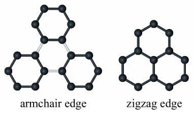
Most of the calculations reported in this paper refer to graphene nanotriangles of either armchair or zigzag edges centered around the middle point of a carbon hexagon. We consider the edge atoms to be passivated with hydrogen, and therefore, we treat them as the rest of the atoms in the structure, with the same hopping to their nearest neighbors. The number of atoms in the nanotriangles is for armchair edges and for zigzag edges, where is the number of hexagons along the side. For example, the triangles of Fig. 4 contain 18 and 13 carbon atoms, respectively. The side length of the triangles is for armchair edges and for zigzag edges, where nm is the nearest-neighbor distance.
Appendix C Size dependence
We show in Fig. 5 extinction spectra for armchair nanotriangles of two different sizes. The main effect of reducing the size of the graphene island is an increase in the plasmon energies, which is significantly larger than the dependence on side length predicted by a classical electromagnetism description Christensen et al. (2012). However, like in classical theory, the absorption cross-section produced by these plasmons is roughly proportional to the area.
Appendix D Collective character of the plasmons
In the random-phase approximation (RPA) here used to describe the optical response of graphene nanoislands, the induced density is writen as in terms of the external potential , the Coulomb interaction between atomic sites , and the noninteracting RPA susceptibility Thongrattanasiri et al. (2012a) (see Appendix A). The collective character of the plasmons is clearly captured in a multiple-scattering fashion by the use of the self-consistent potential in the above expression. We compare in Fig. 5 these full RPA calculations (Fig. 5c,d) with those obtained by removing the self-consistency and calculating the induced charge as (Fig. 5e,f). This leads to dramatic changes in the plasmon spectrum: the plasmon dispersion with varying doping charge is removed, and the spectral features are now peaked at the positions of dominant electron-hole-pair transitions (see Fig. 3c). This is in contrast to the plasmons obtained from self-consistent calculations, the energies of which depend on the interaction among different electron-hole-pair virtual transitions, as a manifestation of the collective electron motion involved in these excitations.
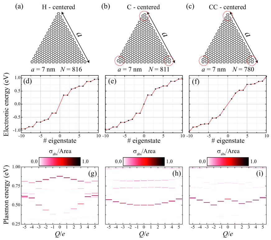
Appendix E Dependence on the choice of triangle center
Plasmons in graphene nanoislands are very sensitive to small structural details of the carbon lattice. Besides the strong dependence on the type of edges observed in Fig. 2, we show in Fig. 6 a large variation in the plasmonic spectrum with the position of the triangle center. In Fig. 6a,d,g and in the rest of the figures of this work, we present calculations obtained with the center located at the middle point of a carbon hexagon (H-centered). When the triangle center is chosed at a carbon site (C-centered, Fig. 6b,e,h) or at the center of a nearest-neighbors bond (C-C-centered, Fig. 6c,f,i), the corners of the atomic structure present a certain degree of asymmetry (see Fig. 6b,c) and the one-electron energies are substantially modified (Fig. 6e,f). This leads to dramatic changes in the extinction spectra (Fig. 6h,i), which are still exhibiting a clear plasmon dispersion with varying doping charge. In particular, the lowest-energy plasmon of the C-C-centered triangle (Fig. 6i) shows a bump in energy at zero doping, in contrast to the lowest-energy plasmon of the H-centered triangle (Fig. 6g), which steadily increases in energy with doping.
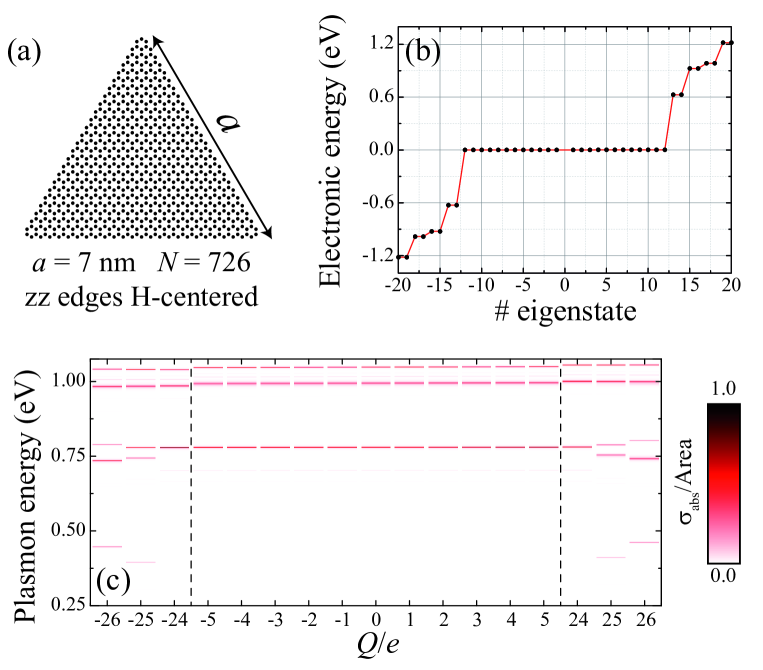
Appendix F Effect of zigzag edges and zero-energy electronic states
Zigzag edges are known to produce electron states near the Dirac point that are concentrated near the atomic edges. The number of such states is equal to the difference between the number of atoms in the two carbon sublattices of the graphene nanostructure Fernández-Rossier and Palacios (2007); Akhmerov and Beenakker (2008); Wimmer et al. (2010). This is the case of the C-centered triangle of Fig. 6b, which contains zigzag edges near the corners that lead to the existence of one zero-energy state. This state is half-filled in the neutral structure. Interestingly, adding or removing a single electron to the nanotriangle does not produce any significant change in the plasmonic spectrum because it ends up in an edge-localized electronic state that cannot undergo large dipole transitions. However, the addition or removal of two electrons causes a sizeable shift. One can therefore speculate that electrons added (removed) to (from) the zero-energy states have no effect in the collective plasmon excitations. Another piece of evidence pointing to this direction is provided by the zigzag triangle considered in Fig. 3b,d,f, which contains a large number of zero-energy states and does not suffer any plasmon shifts with the addition of a small number of electrons or holes. In order to test this hypothesis, we consider the same zigzag triangle in Fig. 7, subject now to much higher doping. Interestingly, the plasmonic spectrum remains nearly unchanged while electrons or holes are added to the nanoisland. However, when the zero-energy states are completely filled (depleted) and further electrons (holes) are added to the structure, the plasmons undergo strong variations in energy with every new electron (hole). This is strong evidence that zero-energy states do not contribute to plasmons, and the tunability observed in graphene islands with varying doping is quenched by the presence of these states. In summary, zigzag edges produce a net difference in the number of atoms in the two carbon sublattice of graphene nanoislands, leading to the presence of zero-energy states localized near the edges, the optical excitation of which is rather inefficient because they cannot undergo large dipole transitions, and therefore, zigzag edges are detrimental to the tunability of graphene plasmons via doping.
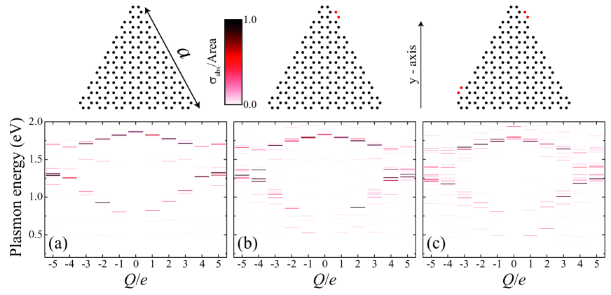
Appendix G Effect of disorder in the edges
The robustness of the spectra of armchair nanotriangles is tested in Fig. 8 against the degree of disorder in the edges. In particular, this figure shows that the spectral features of an immaculate doped nm triangle are increasingly split as extra atoms are added to the edges. Additionally, low-energy features are becoming more intense. Incidentally, the number of atoms in both carbon sublattices remains the same in all the structures considered in Fig. 8 (i.e., the two atoms added in each step belong to different sublattices), so that there are neither zero-energy states nor effects associated with dummy zero-energy electrons, as described in the previous section.
Appendix H Formation of the Dirac cone in large islands
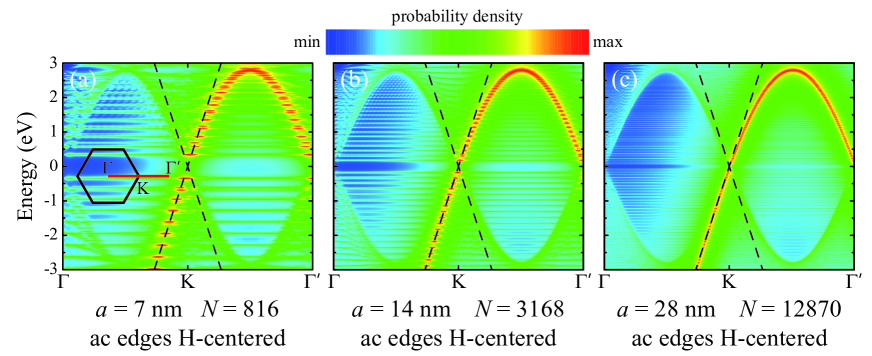
We show in Fig. 9 the formation of the Dirac cone structure as the size of the nanotriangle is increased. The Dirac cone emerges in the momentum-energy representation of the electronic bands in extended graphene. However, the momentum is not a good quantum number in finite nanoislands due to the lack of translational symmetry. Instead, we have taken the spatial Fourier transform of each and all of the one-electron states and represented the sum of their intensities as a function of wave vector. This produces an energy-momentum structure that is reminiscent of the Dirac cone, which is more clearly emerging as the size of the nanotriangles increases.
Appendix I Maximum absorption cross-section
The absorption cross-section at the peak of the features associated with the excitation of plasmons can exceed the geometrical area of the graphene. We show this in Fig. 10 for the plasmons of the island considered in Fig. 2a. These cross-sections are thus large enough to produce complete optical absorption in a surface decorated with nanoislands Thongrattanasiri et al. (2012b). Importantly, the maximum cross-section is directly proportional to the intrinsic decoherence time , which can be increased due to thermal and disorder effects Jablan et al. (2009). Nonetheless, our choice of meV is compatible with estimates based upon reported DC mobilities for high-quality graphene Jablan et al. (2009).
References
- Nie and Emory (1997) S. Nie and S. R. Emory, Science 275, 1102 (1997).
- Kneipp et al. (1997) K. Kneipp, Y. Wang, H. Kneipp, L. T. Perelman, I. Itzkan, R. R. Dasari, and M. S. Feld, Phys. Rev. Lett. 78, 1667 (1997).
- Johansson et al. (2005) P. Johansson, H. Xu, and M. Käll, Phys. Rev. B 72, 035427 (2005).
- Talley et al. (2005) C. E. Talley, J. B. Jackson, C. Oubre, N. K. Grady, C. W. Hollars, S. M. Lane, T. R. Huser, P. Nordlander, and N. J. Halas, Nano Lett. 5, 1569 (2005).
- Rodríguez-Lorenzo et al. (2009) L. Rodríguez-Lorenzo, R. A. Álvarez-Puebla, I. Pastoriza-Santos, S. Mazzucco, O. Stéphan, M. Kociak, L. M. Liz-Marzán, and F. J. García de Abajo, J. Am. Chem. Soc. 131, 4616 (2009).
- Qian et al. (2008) X. Qian, X.-H. Peng, D. O. Ansari, Q. Yin-Goen, G. Z. Chen, D. M. Shin, L. Yang, A. N. Young, M. D. Wang, and S. Nie, Nat. Biotech. 26, 83 (2008).
- Hirsch et al. (2003) L. Hirsch, R. Stafford, J. Bankson, S. Sershen, B. Rivera, R. Price, J. Hazle, N. Halas, and J. West, Proc. Natl. Acad. Sci. 100, 13549 (2003).
- Asahi et al. (2001) R. Asahi, T. Morikawa, T. Ohwaki, K. Aoki, and Y. Taga, Science 293, 269 (2001).
- Kamat (2002) P. V. Kamat, J. Phys. Chem. B 106, 7729 (2002).
- Grzelczak et al. (2008) M. Grzelczak, J. Pérez-Juste, P. Mulvaney, , and L. M. Liz-Marzán, Chem. Soc. Rev. 37, 1783 (2008).
- Chapman and Mulvaney (2001) R. Chapman and P. Mulvaney, Chem. Phys. Lett. 349, 358 (2001).
- Hirakawa and Kamat (2004) T. Hirakawa and P. V. Kamat, Langmuir 20, 5645 (2004).
- Castro Neto et al. (2009) A. H. Castro Neto, F. Guinea, N. M. R. Peres, K. S. Novoselov, and A. K. Geim, Rev. Mod. Phys. 81, 109 (2009).
- Ju et al. (2011) L. Ju, B. Geng, J. Horng, C. Girit, M. Martin, Z. Hao, H. A. Bechtel, X. Liang, A. Zettl, Y. R. Shen, et al., Nat. Nanotech. 6, 630 (2011).
- Fei et al. (2011) Z. Fei, G. O. Andreev, W. Bao, L. M. Zhang, A. S. McLeod, C. Wang, M. K. Stewart, Z. Zhao, G. Dominguez, M. Thiemens, et al., Nano Lett. 11, 4701 (2011).
- Yan et al. (2012a) H. Yan, X. Li, B. Chandra, G. Tulevski, Y. Wu, M. Freitag, W. Zhu, P. Avouris, and F. Xia, Nat. Nanotech. 7, 330 (2012a).
- Yan et al. (2012b) H. Yan, T. Low, W. Zhu, Y. Wu, M. Freitag, X. Li, F. Guinea, P. Avouris, and F. Xia, arXiv 0, arXiv:1209.1984v1 (2012b).
- Chen et al. (2012) J. Chen, M. Badioli, P. Alonso-González, S. Thongrattanasiri, F. Huth, J. Osmond, M. Spasenović, A. Centeno, A. Pesquera, P. Godignon, et al., Nature 487, 77 (2012).
- Fei et al. (2012) Z. Fei, A. S. Rodin, G. O. Andreev, W. Bao, A. S. McLeod, M. Wagner, L. M. Zhang, Z. Zhao, M. Thiemens, G. Dominguez, et al., Nature 487, 82 (2012).
- Emani et al. (2012) N. K. Emani, T.-F. Chung, X. Ni, A. V. Kildishev, Y. P. Chen, and A. Boltasseva, Nano Lett. 12, 5202 (2012).
- Fang et al. (2012a) Z. Fang, Z. Liu, Y. Wang, P. M. Ajayan, P. Nordlander, and N. J. Halas, Nano Lett. 12, 3808 (2012a).
- Fang et al. (2012b) Z. Fang, Z. Liu, Y. Wang, P. M. Ajayan, P. Nordlander, and N. J. Halas, ACS Nano 6, 10222 (2012b).
- Pines and Nozières (1966) D. Pines and P. Nozières, The Theory of Quantum Liquids (W. A. Benjamin, Inc., New York, 1966).
- Thongrattanasiri et al. (2012a) S. Thongrattanasiri, A. Manjavacas, and F. J. García de Abajo, ACS Nano 6, 1766 (2012a).
- Wallace (1947) P. R. Wallace, Phys. Rev. 71, 622 (1947).
- Wunsch et al. (2006) B. Wunsch, T. Stauber, F. Sols, and F. Guinea, New J. Phys. 8, 318 (2006).
- Brey and Fertig (2007) L. Brey and H. A. Fertig, Phys. Rev. B 75, 125434 (2007).
- Jablan et al. (2009) M. Jablan, H. Buljan, and M. Soljac̆ić, Phys. Rev. B 80, 245435 (2009).
- Novoselov et al. (2004) K. S. Novoselov, A. K. Geim, S. V. Morozov, D. Jiang, Y. Zhang, S. V. Dubonos, I. V. Grigorieva, and A. A. Firsov, Science 306, 666 (2004).
- Novoselov et al. (2005) K. S. Novoselov, A. K. Geim, S. V. Morozov, D. Jiang, M. I. Katsnelson, I. V. Grigorieva, S. V. Dubonos, and A. A. Firsov, Nature 438, 197 (2005).
- Armbrust et al. (2012) N. Armbrust, J. Güdde, P. Jakob, and U. Höfer, Phys. Rev. Lett. 108, 056801 (2012).
- Peres et al. (2010) N. M. R. Peres, R. M. Ribeiro, and A. H. Castro Neto, Phys. Rev. Lett. 105, 055501 (2010).
- Fernández-Rossier and Palacios (2007) J. Fernández-Rossier and J. J. Palacios, Phys. Rev. Lett. 99, 177204 (2007).
- Ezawa (2007) M. Ezawa, Phys. Rev. B 76, 245415 (2007).
- Akhmerov and Beenakker (2008) A. R. Akhmerov and C. W. J. Beenakker, Phys. Rev. B 77, 085423 (2008).
- Zhang et al. (2008) Z. Z. Zhang, K. Chang, and F. M. Peeters, Phys. Rev. B 77, 235411 (2008).
- Wimmer et al. (2010) M. Wimmer, A. R. Akhmerov, and F. Guinea, Phys. Rev. B 82, 045409 (2010).
- Zarenia et al. (2011) M. Zarenia, A. Chaves, G. A. Farias, and F. M. Peeters, Phys. Rev. B 84, 245403 (2011).
- Thongrattanasiri et al. (2012b) S. Thongrattanasiri, F. H. L. Koppens, and F. J. García de Abajo, Phys. Rev. Lett. 108, 047401 (2012b).
- Luo et al. (2011) Y. L. Luo, Y. S. Shiao, and Y. F. Huang, Nat. Nanotech. 6, 247 (2011).
- Subramaniam et al. (2012) D. Subramaniam, F. Libisch, Y. Li, C. Pauly, V. Geringer, R. Reiter, T. Mashoff, M. Liebmann, J. Burgdörfer, C. Busse, et al., Phys. Rev. Lett. 108, 046801 (2012).
- Kim et al. (2012) S. Kim, S. W. Hwang, M.-K. Kim, D. Y. Shin, D. H. Shin, C. O. Kim, S. B. Yang, J. H. Park, E. Hwang, S.-H. Choi, et al., ACS Nano 6, 8203 (2012).
- Kobayashi et al. (2005) Y. Kobayashi, K. ichi Fukui, T. Enoki, K. Kusakabe, and Y. Kaburagi, Phys. Rev. B 71, 193406 (2005).
- Tian et al. (2011) J. Tian, H. Cao, W. Wu, Q. Yu, and Y. P. Chen, Nano Lett. 11, 3663 (2011).
- Ç. Ö. Girit et al. (2009) Ç. Ö. Girit, J. C. Meyer, R. Erni, M. D. Rossell, C. Kisielowski, L. Yang, C.-H. Park, M. F. Crommie, M. L. Cohen, S. G. Louie, et al., Science 27, 1705 (2009).
- Shu et al. (2012) H. Shu, X. Chen, X. Tao, and F. Ding, ACS Nano 6, 3243 (2012).
- Gan and Srolovitz (2010) C. K. Gan and D. J. Srolovitz, Phys. Rev. B 81, 125445 (2010).
- Wu et al. (2007) J. Wu, W. Pisula, and K. Müllen, Chem. Rev. 107, 718 (2007).
- Feng et al. (2008) X. Feng, M. Liu, W. Pisula, M. Takase, J. Li, and K. Müllen, Adv. Mater. 20, 2684 (2008).
- Schedin et al. (2007) F. Schedin, A. K. Geim, S. V. Morozov, E. W. Hill, P. Blake, M. I. Katsnelson, and K. S. Novoselov, Nat. Mater. 6, 652 (2007).
- Bharadwaj et al. (2011) P. Bharadwaj, A. Bouhelier, , and L. Novotny, Phys. Rev. Lett. 106, 226802 (2011).
- Kundu et al. (2008) J. Kundu, F. Le, P. Nordlander, and N. J. Halas, Chem. Phys. Lett. 452, 115 (2008).
- Koppens et al. (2011) F. H. L. Koppens, D. E. Chang, and F. J. García de Abajo, Nano Lett. 11, 3370 (2011).
- Bostwick et al. (2007) A. Bostwick, T. Ohta, T. Seyller, K. Horn, and E. Rotenberg, Nat. Phys. 3, 36 (2007).
- Bolotin et al. (2008) K. I. Bolotin, K. J. Sikes, Z. Jiang, M. Klima, G. Fudenberg, J. Hone, P. Kim, and H. L. Stormer, Sol. State Commun. 146, 351 (2008).
- Christensen et al. (2012) J. Christensen, A. Manjavacas, S. Thongrattanasiri, F. H. L. Koppens, and F. J. García de Abajo, ACS Nano 6, 431 (2012).