Quantized Conductance and Field-Effect Topological Quantum
Transistor
in Silicene Nanoribbons
Abstract
Silicene (a monolayer of silicon atoms) is a quantum spin-Hall insulator, which undergoes a topological phase transition into other insulators by applying external field such as electric field, photo-irradiation and antiferromagnetic order. We investigate the electronic and transport properties of silicene nanoribbons based on the Landauer formalism. We propose to determine topological phase transitions by measuring the density of states and conductance. The conductance is quantized and changes its value when the system transforms into different phases. We show that a silicene nanoribbon near the zero energy acts as a field-effect transistor. This transistor is robust though it makes use of the minimum quantized conductance since the zero-energy edge states are topologically protected. Our findings open a new way to future topological quantum devices.
Silicene is a honeycomb structure of silicon atoms akin to graphene. Its experimental synthesis has opened a breakthrough in the study of siliceneGLayPRL ; Takamura ; Kawai . It has two salient features absent in graphene. One is the relatively large spin-orbit (SO) interaction, which enables quantum spin-Hall (QSH) effects to realizeLiuPRL . The other is its buckled structure, which enable us to apply different external fields between the A and B sublattices such as electric field and exchange field. As a result we can externally tune the band gap of silicene and drive topological phase transitions from the QSH insulator to other insulatorsEzawaNJP ; EzawaQAH ; EzawaPhoto . We have already shown how to make experimental observation of phase transition points with the use of diamagnetismDiamag and also optical absorptionEzawaOpt . However, these methods may not be so practical.
The most important graphene derivative is nanoribbonFujita ; EzawaRibbon ; Brey . The low-bias low-temperature conductance of graphene nanoribbons has been shownPeres to be quantized as
| (1) |
both for zigzag and armchair edges. We interpret the formula to imply the electron-hole symmetry, the 4-fold degeneracy of each energy level associated with the spin and valley degrees of freedom, and the conductance quantum per channel. It is interesting to examine the same problem in silicene nanoribbons because the spin-valley degeneracy is broken according to a specific pattern in each phase.
Topological insulators are indexedProdan ; Hasan ; Qi by a set of two topological numbers , where and are the Chern number and the spin-Chern number modulo . There appear four types of insulators in siliceneEzawaQAH ; EzawaPhoto ; Ezawa2Ferro . They are the QSH, the quantum anomalous Hall (QAH), the spin-polarized quantum anomalous Hall (SQAH), and the trivial band insulators. The QSH effect is an analogue of the quantum Hall effect for spin currents instead of charge currents. The QAH effect is the quantum Hall effect without Landau levels, while the SQAH insulator has a hybrid character of the QSH and QAH insulators. The prominent feature of a topological insulator is the emergence of zero-energy edge states at half-filling which are topologically protected against perturbationHasan ; Qi .
In this paper we calculate the density of states (DOS) and the conductance in zigzag silicene nanoribbons based on the Landauer formalismDatta , and propose an experimentally better method to detect a topological phase transition by way of measuring them. Our first observation is that there are finite DOS due to the zero-energy edge states in a topological phase, while they are absent in the trivial phase. Consequently, the topological phase transition must be observed experimentally just by measuring the site-resolved DOS with controlled electric field, which can be achieved by spatially resolved the scanning tunneling microscope/scanning tunneling spectroscopy (STM/STS).
The particularly important quantity is the conductance due to the topologically protected zero-energy edge channels, which is the one experimentally observable. It is interesting that the helical edge of the QSH and the chiral edge of the QAH insulators have the same amount of conductance. Our result is summarized as
| (2) |
The conductance changes its quantized value when the system is transformed into different phases by tuning electric field. Because of this property a silicene nanoribbon may act as a field-effect transistor, where the conductance is quantized and topologically protected.
Hamiltonian: The basic nature of silicene is described by the tight-binding HamiltonianKaneMele ; LiuPRB ,
| (3) |
where creates an electron with spin polarization at site in a honeycomb lattice, and run over all the nearest/next-nearest-neighbor hopping sites. The first term represents the usual nearest-neighbor hopping with the transfer energy eV. The second term represents the effective SO interaction with meV, and if the next-nearest-neighboring hopping is anticlockwise and if it is clockwise with respect to the positive axis. We have neglected the Rashba interactions since their effects are negligibly smallEzawaQAH in general. Here, is the Pauli matrix for the the component of the spin, whose eigenvalues are . We also use for indices.
There are two inequivalent Brillouin zone corners, called the and points, as in graphene. The conduction and valence bands form two conically shaped valleys or cones at these points. We assign the valley index to electrons at the or point, and call them the points as well. We also use for indices. The low-energy effective Hamiltonian is given by the massive Dirac theory around the point. The Hamiltonian (3) yields
| (4) |
where is the Fermi velocity with the lattice constant Å. Here, is the Pauli matrix for the component of the pseudospin representing the and sublattices, whose eigenvalues are .
A great merit of silicene is that we can introduce various potential terms into the Hamiltonian by making advantages of its bucked structure. Eight commuting terms are possible in the Dirac Hamiltonian (4),
| (5) |
where or . Each term has different symmetry properties. The coefficient of is the Dirac mass, to which four terms contribute. They are . First, is nothing but the SO coupling term with . Second, is the staggered sublattice potential termEzawaNJP with , where is the separation between the and sublattices and is the external electric field. Third, is the Haldane termHaldane , where we set by introducing photo-irradiationEzawaPhoto ; Kitagawa with strength . Finally, is the the staggered exchange termEzawa2Ferro , where we set by introducing the exchange fields to the -sublattice.
We may write down the tight-binding term that yields the potential term . The additional terms areEzawaNJP ; EzawaQAH ; Ezawa2Ferro
| (6) |
where for . The Dirac Hamiltonian is
| (7) |
The spin-valley dependent Dirac mass is given by
| (8) |
It may be positive, negative or zero. The silicene system is described by the Hamiltonian .
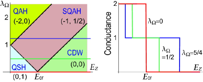
Topological phases: Any insulating state is characterized by a set of two topological quantum numbers . Provided the spin is a good quantum number, they are given by and , where is the summation of the Berry curvature in the momentum space over all occupied states of electrons with spin in the Dirac valley , and calculatedDiamag as sgn. All possible topological insulators are determined by the three parameters , and with respect to . Possible sets of topological numbers are up to the sign . They are the trivial, QAH, QSH, SQAH insulators, respectively. Note that there are two-types of trivial band insulators, which are the charge-density-wave (CDW) type insulator and the antiferromagnetic (AF) insulatorEzawa2Ferro .
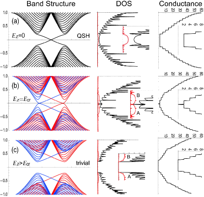
A topological phase transition occurs when the band gap closes, or . Let us reviewEzawaNJP the topological phase transition along the axis, where the Dirac mass is given by . The condition implies with . It follows that for and for . We have given the band structures at , and in Fig.2. It is the characteristic feature known as the bulk-edge correspondence that zero-energy edge modes emerge in topological insulators with and that these zero-energy edge modes are topologically protected against perturbationHasan ; Qi .
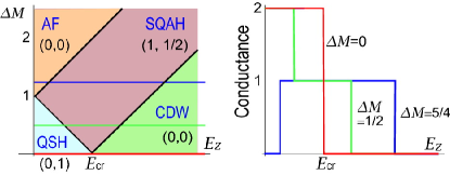
We may easily construct the phase diagrams by solving . Those in the space and the space are given in Figs.3 and 4 together with the pair of topological charges , respectively. All possible topological insulators are found in these phase diagrams. The band structures at typical states are found in Figs.2 and 5, where the breakdown of the spin-valley symmetry is manifest. We proceed to characterize each phase by its characteristic pattern of the DOS and the conductance of a zigzag nanoribbon.
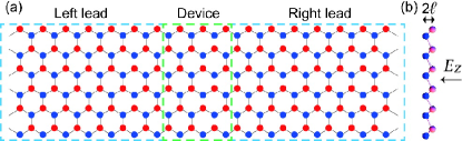
DOS and conductance: The natural framework for transport calculations in nanoscopic devices is the Landauer formalismDatta . We consider a zigzag silicene nanoribbon divided into three regions [Fig.1]: the device region, the left lead and the right lead. The size of the device region is actually irrelevant due to the ballistic transport property.
In terms of single-particle Green’s functions, the low-bias conductance at the Fermi energy is given byDatta
| (9) |
where with the self-energies and , and
| (10) |
with the Hamiltonian for the device region. The self-energy describes the effect of the electrode on the electronic structure of the device, whose real part results in a shift of the device levels whereas the imaginary part provides a life time. It is to be calculated numericallySancho ; Rojas ; Nikolic ; Li .
The total density of states (DOS) reads
| (11) |
while the partial density of states at site reads
| (12) |
in terms of the Green function of the device.
We have calculated the DOS and the conductance of a nanoribbon as functions of the Fermi energy , which is controlled by doping. We give the results at electric field , and in Fig.2. A van Hove singularity occurs in the DOS at the point where the band dispersion is flat. As increases beyond the point, the Fermi level crosses a new band. A new channel opens and contributes to the conductance by for each spin and valley. It is clearly observed that the edge channel connects the tips of the Dirac cones with the same spin at the and points.
We have also plotted the site-resolved DOS of the up-spin states at the outmost and sites of a nanoribbon by red curves in the insets [Fig.2]. They represent degenerate zero-energy states at . As we have explained in Fig.1, the energy of the and sites become different for . It results in the downward (upward) shift of along the edge as increases. They are separated completely, and zero-energy states disappear for .
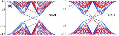
The zero-energy edge channel of a topological insulator is particularly important at half-filling, because it is topologically protected. We have calculated the conductance at half-filling by increasing the external field in the space and the space. First, we increase from at in the space [Fig.3]. Initially the conductance reads for , where the system is in the QSH phase. It reads , when the system is in the SQAH phase. Its band structure is shown in Fig.5(a), where the zero-energy edge states account for the conductance . The conduction becomes zero as increases and the system becomes the trivial AF insulator.
We confirm these observations by investigating the same problem in the space [Fig.4]. The system is in the QAH phase for at , where . We illustrate the band structure of the QSH insulator in Fig.5(b), where the zero-energy edge states account for the conductance . The edge channel is helical (chiral) in the QSH (QAH) phase, but both of them transport the same amount of electric charges when the current is fed. We summarize the conductance in each topological insulator as in (2).
Field-effect topological quantum transistor: The conductance is quantized in silicene nanoribbons. The simplest system is provided by applying electric field onlyEzawaNJP , where quantized conductance changes from to at the critical electric field . This means the system acts as a transistor where "on" state can be switched off to "off" state by applying electric field. This transistor is "quantum" since the conductance is quantized, which is highly contrasted with the ordinal transistor, where the conductance is not quantized. Furthermore the conductance is topologically protected because the zero-energy edge state is topologically protected. Namely the conductance is robust against impurities due to its topological stability. Consequently we may call it a field-effect topological quantum transistor. This is the most energy-saving device since it utilizes the minimum conductance.
We are able to design a three-digit quantum transistor by attaching antiferromagnet. Namely the conductance changes in three steps 2, 1, 0 with increasing electric field when . When , the conductance changes in three step 0, 1, 0. It acts as a three-step transistor, where the system is first in the "off" state, then become "on" state and finally become "off" state with the increase of electric field.
Conclusions: We have analyzed the DOS and the conductance in silicene nanoribbons. There are finite DOS due to the zero-energy edge states in the topological phase, while they disappear in the trivial phase [Fig.2]. Local DOS measurement is a direct evidence of the existence of the edge states, which can be achieved by spatially resolved STM/STS. This must be the most efficient way to make an experimental observation of a topological phase transition. Furthermore we can determine the band gap by measuring the DOS. A precise measurement is possible owing to the van-Hove singularities present at the tips of the conduction and valence bands [Fig.2].
Conductance measurement is also a direct method to observe a topological phase transition. We have proposed a field-effect topological quantum transistor with the use of the zero-energy edge state of a silicene nanoribbon. This could be a basic component of future topological quantum devices.
In passing we address the problem how narrow the nanoribbon can be. The penetration depth of the zero-energy edge state has already been shown to be as short as the atomic scaleArm in zigzag nanoribbons. Hence we may use a quite narrow nanoribbon to detect and make use of the topological properties of silicene.
I am very much grateful to N. Nagaosa and B. K. Nikolić for many helpful discussions on the subject. This work was supported in part by Grants-in-Aid for Scientific Research from the Ministry of Education, Science, Sports and Culture No. 22740196.
References
- (1) P. Vogt, , P. De Padova, C. Quaresima, J. A., E. Frantzeskakis, M. C. Asensio, A. Resta, B. Ealet and G. L. Lay, Phys. Rev. Lett. 108, 155501 (2012).
- (2) A. Fleurence, R. Friedlein, T. Ozaki, H. Kawai, Y. Wang, and Y. Yamada-Takamura, Phys. Rev. Lett. 108, 245501 (2012).
- (3) C.-L. Lin, R. Arafune, K. Kawahara, N. Tsukahara, E. Minamitani, Y. Kim, N. Takagi, M. Kawai, Appl. Phys. Express 5, Art No. 045802 (2012) .
- (4) C.-C. Liu, W. Feng, and Y. Yao, Phys. Rev. Lett. 107, 076802 (2011).
- (5) M. Ezawa, New J. Phys. 14, 033003 (2012).
- (6) M. Ezawa, Phys. Rev. Lett. 109, 055502 (2012).
- (7) M. Ezawa, Phys. Rev. Lett. 110, 026603 (2013).
- (8) M. Ezawa, Euro. Phys. J. B 85, 363 (2012).
- (9) M. Ezawa, Phys. Rev. B 86, 161407(R) (2012).
- (10) M. Fujita, et al., J. Phys. Soc. Jpn. 65, 1920 (1996).
- (11) M. Ezawa, Phys. Rev. B 73, 045432 (2006).
- (12) L. Brey and H. A. Fertig, Phys. Rev. B, 73, 235411 (2006).
- (13) N. M. R. Peres, A. H. Castro Neto, and F. Guinea, Phys. Rev. B 73, 195411 (2006).
- (14) E. Prodan, Phys. Rev. B 80, 125327 (2009).
- (15) M.Z Hasan and C. Kane, Rev. Mod. Phys. 82, 3045 (2010).
- (16) X.-L. Qi and S.-C. Zhang, Rev. Mod. Phys. 83, 1057 (2011).
- (17) M. Ezawa, cond-matt/arXiv:1301.0971.
- (18) S. Datta, Electronic Transport in Mesoscopic Systems (Cambridge University Press, Cambridge, England, 1995): Quantum Transport: Atom to Transistor (Cambridge University Press, England, 2005)
- (19) C. L. Kane and E. J. Mele, Phys. Rev. Lett. 95, 226801 (2005); ibid 95, 146802 (2005).
- (20) C.-C. Liu, H. Jiang, and Y. Yao, Phys. Rev. B, 84, 195430 (2011).
- (21) F. D. M. Haldane, Phys. Rev. Lett. 61, 2015 (1988).
- (22) T. Kitagawa, T. Oka, A. Brataas, L. Fu, and E. Demler, Phys. Rev. B 84, 235108 (2011).
- (23) M. P. L. Sancho, J. M. L. Sancho, and J. Rubio, J. Phys. F: Met. Phys. 15, 851 (1985).
- (24) F. Muñoz-Rojas, D. Jacob, J. Fernández-Rossier, and J. J. Palacios, Phys. Rev. B 74, 195417 (2006).
- (25) L. P. Zârbo and B. K. Nikolić EPL, 80 47001 (2007): D. A. Areshkin and B. K. Nikolić Phys. Rev. B 79, 205430 (2009)
- (26) T. C. Li and S.-P. Lu, Phys. Rev. B 77, 085408 (2008).
- (27) M. Ezawa and N. Nagaosa, cond-mat/arXiv:1301.6337.