Phonon Softening and Direct to Indirect Bandgap Crossover in Strained Single Layer MoSe2
Abstract
Motivated by recent experimental observations of Tongay et al. [Tongay et al., Nano Letters, 12(11), 5576 (2012)] we show how the electronic properties and Raman characteristics of single layer MoSe2 are affected by elastic biaxial strain. We found that with increasing strain: (1) the and Raman peaks ( and in bulk) exhibit significant red shifts (up to 30 cm-1), (2) the position of the peak remains at 180 cm-1 ( in bulk) and does not change considerably with further strain, (3) the dispersion of low energy flexural phonons crosses over from quadratic to linear and (4) the electronic band structure undergoes a direct to indirect bandgap crossover under 3 biaxial tensile strain. Thus the application of strain appears to be a promising approach for a rapid and reversible tuning of the electronic, vibrational and optical properties of single layer MoSe2 and similar MX2 dichalcogenides.
pacs:
81.16.Pr, 68.65.Pq, 66.30.Pa, 81.05.ueI Introduction
The discovery of graphenenovo ; geim is expected to play an important role in future nanoscience and nanotechnology applications. Recent advances in nanoscale growth and mechanical exfoliation techniques have led not only to the fabrication of high-quality graphenes but also the emergence of several new classes of two-dimensional (2D) structures such as ultra-thin transition metal dichalcogenides (TMDs). Just like graphene TMDs have hexagonal crystal structure composed of layers of metal atoms (M) sandwiched between layers of chalcogen atoms (X) with stoichiometry MX2. TMDs have electronic semiconducting or metallic properties and most of bulk TMDs possess indirect band gaps of the order 1-2 eV gap . The synthesis of several TMDs has been realized experimentally science 2011 ; prb-2002 ; novo-pnas-2005 ; nature-nano and the stability and electronic properties of various single layer dichalcogenides was recently reported.mx2 Recent studies of several semiconducting TMDs such as MoS2, WS2, MoTe2 and MoSe2 have shown that the band gap increases and transforms to a direct band gap with decreasing number of layers.nature-nano ; PRL-105 ; prb84 ; apl99 These sizeable band gaps make them well suited for electronic applications such as transistors, photodetectors and electroluminescent devices. Another unique feature of two-dimensional ultra-thin materials is the possibility to apply large reversible elastic strain. It has been shown that graphene can be strained up to 20 of its ideal structure with only small changes in its electronic band structure, which is in contrast to TMDs.Bull.Mater ; prb-2011 ; yun ; sca
The most recent efforts have been directed towards the synthesis and manipulation of molybdenum diselenide (MoSe2) single layers. In addition to preliminary reports on synthesis of few-layer MX2 structurescondens-mat ; apl-sefa , Tongay et al. demonstrated that a single layer of MoSe2 possesses a direct optical gap of 1.55 eV and exhibits good thermal stability.sefamose2 However, to our knowledge, no research exists addressing the question of how electronic properties and lattice dynamics of single layer MoSe2 are affected by strain. In the present work, we investigate the effect of biaxial strain on the electronic and vibrational properties of single layer MoSe2 structures. Our calculations revealed that applying biaxial strain is able to tune the Raman characteristics and electronic band structure of single layer MoSe2. We expect that this study will offer new opportunities for strain-engineered nanoscale optoelectronic device applications.
II Computational METHODOLOGY
Calculations of physical properties of equilibrium and strained structures were carried out in the framework of density functional theory (DFT), using the plane-wave self-consistent field (PWSCF) code as implemented in the QUANTUM-ESPRESSO package quantumespresso . The generalized gradient approximation (GGA) of Perdew-Burke-Ernzerhof (PBE) was used for the exchange-correlation potential pbe . A plane-wave kinetic energy cutoff of 40 Ry and density cutoff of 400 Ry were used. Brillouin zone integration was performed using a shifted 27271 Monkhorst-Pack meshkpoint . To eliminate the interaction emerging from periodic boundary conditions calculations are performed with a large unitcell including 12 Å vacuum space between adjacent MoSe2 single layers. Ground states and total energies of all systems were obtained after full geometry relaxation with forces on the atoms smaller than 0.02 eV/Å. Phonon frequencies and phonon eigenvectors were calculated in a 441 q-grid using the density functional perturbation theory (DFPT).dfpt
III results and Discussion
III.1 Single Layer MoSe2
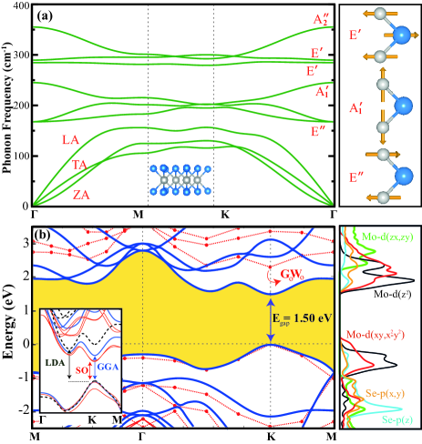
Atomically thin MoSe2 is the most recently synthesized member of the ultra-thin transition metal dichalcogenides. A single layer structure of MoSe2 can be viewed as a 3-layer stacking of Mo and Se atoms wherein molybdenum atoms are sandwiched between layers of trigonally arranged selenium atoms. In this configuration, known as 1H structure, each Mo atom is coordinated to six Se atoms. In the equilibrium geometry of the single layer MoSe2, the Mo-Se distance, the Se-Se distance and the lattice constant of the hexagonal unit cell are calculated to be 2.528, 3.293 and |a|=3.321 Å, respectively. Thus, in comparison with single layer MoS2 having lattice constant 3.12 Å, MoSe2 has a larger atomic structure due to the larger atomic radius of the Se atoms. In Fig. 1(a) we present the calculated phonon dispersion and vibrational characteristics of R-active modes of single layer MoSe2. It is seen that the frequencies of all phonon branches in the whole Brillouin Zone have positive values i.e., MoSe2 crystal can remain stable by generating the required restoring force against atomic distortions. Although the synthesis of single layers of MoSe2 have been achieved only on various substrates so far, energy optimization and phonon dispersion calculations show that freestanding MoSe2 monolayers are quite stable.
The calculated band structure shown in Fig. 1(b) shows that the single layer MoSe2 is a semiconductor with a direct bandgap at the K high symmetry point. The top of the valence band is mainly composed of Mo- orbitals and, albeit small, also by Mo- and Se- orbitals. Though the electrons occupying 4 and 5 shells of a neutral Mo atom are treated as valence electrons, 5 states have a negligible contribution even away from the Fermi level. However, it is seen that all Mo-, Se- and Se- orbitals are hybridized to form the conduction band edge. Note that and component of the orbitals have the same energy due to the two-dimensional lattice symmetry. Due to the presence of another minimum in the conduction band edge between the and K points we also used local density approximation (LDA) for the exchange correlation functional. Tongay et al.sefamose2 demonstrated that such a neighboring conduction band dip is quite sensitive to temperature-induced strain and layer-layer interaction. The lattice constant of a single-layer MoSe2 is found to be smaller (3.22 Å) in LDA because of the overestimation of the strength of the covalent bonds. The inset of Fig. 1(b) shows a zoom of both LDA, GGA and GGA+SO band structures along the -K-M path in the Brillouin zone. We see a splitting of the band edges at the vicinity of K point when including spin-orbit (SO) interactions. Interestingly, LDA predicts that single layer MoSe2 is an indirect semiconductor where the top of the valence band is at the K point, and the bottom of the conduction band is found to be between the and K points. It appears that the physically correct description of single layer MoSe2 structure that was reported experimentally as a semiconductorsefamose2 with a direct bandgap is achieved by using the GGA functionals. Therefore, in the rest of our study PBE calculations will be employed.
Although our PBE calculation captures the qualitative nature of the band edge states it underestimates the band gap. To correct the band gap we use the approximationhedin ; shishkin ; onida as implemented in the VASP package.kresse ; paw It was shown before that this kind of calculation has to be converged with respect to the vacuum spacing.vacuum ; wirtz We calculate the quasi-particle shifts using (12121) k-point grid with vacuum spacings of 15 Å, 20 Å, 25 Å, and 30 Å and then extrapolate them to infinity in a similar fashion as done in Ref. [ vacuum, ]. Our calculation results in a band gap value of 2.33 eV. Note that, excitonic effects are pronounced in 2D materials as MoSe2 and we need to calculate the binding energy of the exciton in order to estimate the optical gap.wirtz ; exc-mx2 ; qp-mos2 ; bse-mose2 ; cud-prl ; cud-prb Due to the parabolic shape of the conduction and valence bands we assume that the exciton has the Mott-Wannier character and the effective mass approximation can be used. Hole and electron effective masses calculated from the band structure are = 0.65 and = 0.53 (in units of electron mass). Moreover, we account for the 2D polarizability of the system using the model introduced by Cudazzo et al.cud-prb Using parameters reported by Ref. [ exc-mx2, ] we find the binding energy of the exciton 0.7 eV, which is in agreement with the value obtained by solving the Bethe-Salpeter equation.exc-mx2 ; bse-mose2 Combining this with our result from calculation we estimate the optical gap to be 1.63 eV, which is close to the reported experimental value of 1.56 eV.
III.2 Lattice Dynamics and Phonon Softening
While bulk MoSe2 crystal has the D6h point group symmetry, it turns into D3h for single layer structure. Just like in MoS2,phononmos2 lattice vibrations of single layer MoSe2 is characterized by nine phonon branches including three acoustic and six optical branches. Analysis of lattice dynamics shows that the decomposition of the vibration representation at the point is . While LA and TA acoustic branches have linear dispersion, the frequency of the out of plane flexural (ZA) mode has a quadratic dispersion in the vicinity of q=0. Near to the point the in-plane sound velocity of the LA and TA modes are found to be 1.5103 and 0.9103 m/s, respectively. It is also seen that differing from graphene’s phonon dispersion the acoustic and optical modes are well-separated from each other. Differing from MoS2 and WS2 structures in which the mode is the highest Raman-active mode, in MoSe2 the mode is located in between the and modes. In Fig. 1(a) the atomic displacements of the R-active modes are presented. Interestingly, although recent Raman spectroscopy measurements of Tongay et al.sefamose2 revealed that only one characteristic Raman peak of single-layer MoSe2 is observable at 240 cm-1, our symmetry analysis predicts the existence of two more Raman-active modes. Significantly decreased intensity of Raman peak around 290 cm-1 can be explained by considering the coupling of in-plane counter-phase vibration of MoSe2 with the SiO2/Si substrate. Moreover, in experiment the disappearance of ( in bulk) Raman shift around 170 cm-1 is due to the inactivity of this vibrational mode to normally incident light.
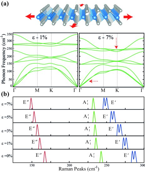
Recent experiments on graphene and other few-layer materials have revealed that the application of biaxial and uniaxial tensile stress is possible by using flexible substrates. We will investigate now how the lattice dynamics of single layer MoSe2 is affected by biaxial strain.
Fig. 2 shows phonon dispersion curves and the evolution of Raman peaks as a function of applied strain. Below 1% strain, the branch of single layer MoSe2 experiences 10 cm-1 softening which is larger than that of the mode (diatomic corresponding to ) of graphene.moh ; hua ; zab It is seen that the low-energy flexural phonons (ZA) of unstrained single layer MoSe2 turns almost in a linear dependence under 7 strain. Such a change in phonon dispersion implies a significant decrease in scattering of electrons by the flexural phonons and an increase in electron mobility for strained MoSe2. For the mode there is a small splitting at the point, as in slightly polar materials such as MoS2 and WS2.phononmos2 It is also seen that due to the weakening of the covalent bonds under strain the and modes (that correspond to the and in bulk MoSe2, respectively) exhibit significant red shifts of about 30 cm-1. Especially, at the K point, the highest optical mode dips even below the band corresponding to the mode. Another remarkable point is the mode (corresponding to the in bulk) that vibrates perpendicular to the applied strain which experiences a smaller softening and is almost pinned to 231 cm-1 for strain values higher than 1. Similar direction-dependent softening behavior was observed for various types of materials.C60 ; lan
III.3 Strain-Induced Direct-to-Indirect Bandgap Crossover
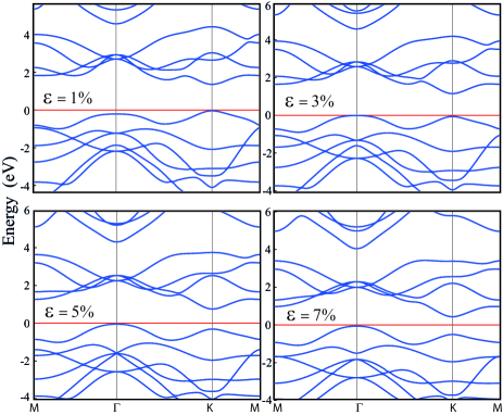
In addition to strain-induced changes in the lattice dynamics, the electronic properties of single layer MoSe2 may exhibit surprising deviations. Existence of a bandgap even in the monolayer structure shows strong bonding nature and the covalent character of MoSe2 layers. Though the covalent bonds formed from valance electrons of Mo and Se atoms are not broken by elastic strain, the strength of the bond is weaken with the increasing distance. Therefore band energies and dispersion can be expected to be strongly dependent on tensile strain. Evolution of the electronic band dispersion under finite biaxal strain () is shown in Fig. 3. It is clearly seen that the band edges at the and K symmetry points are influenced significantly by biaxial tensile strain. Up to 3 strain, single layer MoSe2 remains a direct bandgap semiconductor with both the top of the valence band and the bottom of the conduction band located at the K point. However, when 3 strain is applied, as a result of the band shifting at the K point, two valence band edges with the same energy appear in the Brillouin Zone while the conduction band edge remains fixed in its original position. Here, with 3 strain one has both a direct (KK) and an indirect (K) bandgap.
Such an interesting electronic structure may result in the presence of two types of holes having different effective masses and the coexistence of direct and indirect band transitions in the optical spectra. We also found that increasing further the strain results in the separation (and shifting) of the uppermost valence band towards the conduction band accompanied by the lowering of the conduction band dip at the K point. Moreover, the second conduction band edge located (between and K) very close to the dip of the conduction band at the K point moves upwards in energy. In addition, band edges of MoS2 also experiences similar effects with increasing tensile strain.yun ; sca The evolution of direct (KK) and indirect (KK and K) energy bandgaps under tensile stress are presented in Fig. 4(a). Both direct and indirect bandgaps decrease monotonically with increasing strain, however the rate of decrease is faster for the indirect bandgap. Note that, the variation of band gaps with increasing strain has the same qualitative behavior for PBE, PBE+SO and PBE+ calculations. We predict that the direct-to-indirect crossover takes place at 3-4 strain.
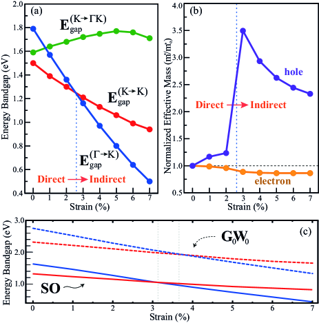
As a consequence of the strain-dependent transition of the valence band edge from the K to point the effective mass of the holes (and electrons) propagating through the single layer MoSe2 lattice changes dramatically. From Fig. 4, it is seen that while the mass of the electrons at the band edge does not change notably, the hole mass shows significant deviations under strain. Since the valence band edge is sharpened by biaxial strain the effective mass of the holes is decreased and after the bandgap crossover holes belong to the uppermost valence band at the point inversely affected by increasing strain. Note that the holes under 7 strain are 2 times heavier than that for unstrained single layer MoSe2.
In summary, motivated by the recent experimental study of Tongay et al.sefamose2 on single layer MoSe2 we investigated the electronic properties and lattice dynamics of single layer MoSe2 as a function of biaxial strain. We showed that GGA describes more accurately the electronic structure of single layer MoSe2 and that LDA predicts the wrong nature of the bandgap. We found that monolayer MoSe2 has four R-active characteristic modes: among these, the modes having counter-phase in-plane motion are significantly modified by strain and they soften by increasing strain. Red-shift in the position of these resonant Raman peaks are predicted to be 30 cm-1. However the branch (corresponds to the in bulk) is negligibly influenced by strain. Moreover the linear dispersion of flexural mode in strained-MoSe2 implies a reduced scattering of electrons from these ZA phonons. Our findings also revealed that the electronic band structure of single layer MoSe2 also undergoes substantial changes under biaxial tensile strain. While the direct bandgap linearly decreases up to 3 tensile strain, a direct to indirect bandgap crossover occurs when strain is further increased. Moreover the appearance of a positive curvature at the K point in the phonon spectra and possible metallicity for higher strain values suggests superconductivity in highly strained single layer MoSe2. Our findings indicate that the bandgap of single layer MoSe2 can be tuned reversibly by biaxial strain and is able to capture a broad range of the solar spectrum.
IV Acknowledgements
This work was supported by the Flemish Science Foundation (FWO-Vl) and the Methusalem programme of the Flemish government. Computational resources were partially provided by TUBITAK ULAKBIM, High Performance and Grid Computing Center (TR-Grid e-Infrastructure). H. S. is supported by a FWO Pegasus Marie Curie Long Fellowship.
References
- (1) K. S. Novoselov, A. K. Geim, S. V. Morozov, D. Jiang, S. C. Dubonos, I. V. Grigorieva, and A. A. Firsov, Science 306, 666 (2004).
- (2) A. K. Geim and K. S. Novoselov, Nat. Mater. 6, 183 (2007).
- (3) A. D. Yoffe, Annu. Rev. Mater. Sci. 3, 147 (1973).
- (4) K. S. Novoselov, D. Jiang, F. Schedin, T. J. Booth, V. V. Khotkevich, S. V. Morozov, and A. K. Geim, Proc. Natl. Acad. Sci. USA 102, 10451 (2005).
- (5) R. A. Gordon, D. Yang, E. D. Crozier, D. T. Jiang, and R. F. Frindt, Phys. Rev. B 65, 125407 (2002).
- (6) J. N. Coleman, M. Lotya, A. O’Neill, S. D. Bergin, P. J. King, U. Khan, K. Young, A. Gaucher, S. De, R. J. Smith, I. V. Shvets, S. K. Arora, G. Stanton, H. Y. Kim, K. Lee, G. T. Kim, G. S. Duesberg, T. Hallam, J. J. Boland, J. J. Wang, J. F. Donegan, J. C. Grunlan, G. Moriarty, A. Shmeliov, R. J. Nicholls, J. M. Perkins, E. M. Grieveson, K. Theuwissen, D. W. McComb, P. D. Nellist, and V. Nicolosi, Science 331, 568 (2011).
- (7) Q. H. Wang, K. Kalantar-Zadeh, A. Kis, J. N. Coleman, and M. S. Strano, Nature Nanotechnology 7, 699 (2012).
- (8) C. Ataca, H. Sahin, and S. Ciraci, J. Phys. Chem. C 116, 8983 (2012).
- (9) K. F. Mak, C. Lee, J. Hone, J. Shan, and T. F. Heinz, Phys. Rev. Lett. 105, 136805 (2010).
- (10) S. W. Han, H. Kwon,S. K. Kim, S. Ryu, W. S. Yun, D. H. Kim, J. H. Hwang, J.-S. Kang, J. Baik, H. J. Shin, and S. C. Hong, Phys. Rev. B 84, 045409 (2011).
- (11) J. K. Ellis, M. J. Lucero, and G. E. Scuseria, Appl. Phys. Lett. 99, 261908 (2011).
- (12) W. S. Yun, S. W. Han, S. C. Hong, I. G. Kim, and J. D. Lee, Phys. Rev. B 85, 033305 (2012).
- (13) E. Scalise, M. Houssa, G. Pourtois, V. Afanas’ev, and A. Stesmans, Nano Res. 5(1), 43 (2012).
- (14) M. Dave, R. Vaidya, S. G. Patel, and A. R. Jani, Bull. Mater. Sci. 27, 213 (2004).
- (15) A. Ramasubramaniam, D. Naveh, and E. Towe, Phys. Rev. B 84, 205325 (2011).
- (16) S. K. Mahatha, K. D. Patel, and K. S. R. Menon, J. Phys.: Condens. Matter 24, 475504 (2012).
- (17) S. Tongay, S. S. Varnoosfaderani, B. R. Appleton, J. Wu, and A. F. Hebard, Appl. Phys. Lett. 101, 123105 (2012).
- (18) S. Tongay, J. Zhou, C. Ataca, K. Lo, T. S. Matthews, J. Li, J. C. Grossman, and J. Wu, Nano Letters, 12(11), 5576 (2012).
- (19) P. Giannozzi, S. Baroni, N. Bonini, M. Calandra, R. Car, C.Cavazzoni, D. Ceresoli, G. L. Chiarotti, M. Cococcioni, I. Dabo, A. Dal Corso, S. de Gironcoli, S. Fabris, G. Fratesi, R. Gebauer, U. Gerstmann, C. Gougoussis, A. Kokalj, M. Lazzeri, L. MartinSamos, N. Marzari, F. Mauri, R. Mazzarello, S. Paolini, A. Pasquarello, L. Paulatto, C. Sbraccia, S. Scandolo, G. Sclauzero, A.P. Seitsonen, A. Smogunov, P. Umari, and R. M. Wentzcovitch, J. Phys.: Condens. Matter 21, 395502 (2009). http://www.quantum-espresso.org
- (20) J. P. Perdew, K. Burke, and M. Ernzerhof, Phys. Rev. Lett. 77, 3865 (1996).
- (21) H. J. Monkhorst and J. D. Pack, Phys. Rev. B 13, 5188 (1976).
- (22) S. Baroni, S. de Gironcoli, A. Dal Corso, and P. Giannozzi, Rev. Mod. Phys. 73, 515 (2001).
- (23) A. Molina-Sanchez and L. Wirtz, Phys. Rev. B 84, 155413 (2011).
- (24) L. Hedin, Phys. Rev. 139, A796 (1965).
- (25) M. Shishkin and G. Kresse, Phys. Rev. B 74, 035101 (2006).
- (26) G. Onida L. Reining, A. Rubio, Rev. Mod. Phys. 74, 601 (2002).
- (27) G. Kresse and J. Hafner, Phys. Rev. B 47, 558 (1993); G. Kresse and J. Furthmüller, Phys. Rev. B 54, 11169 (1996).
- (28) P. E. Blochl, Phys. Rev. B 50, 17953 (1994).
- (29) N. Berseneva, A. Gulans, A. V. Krasheninnikov, and R. M. Nieminen, Phys. Rev. B 87, 035404 (2013).
- (30) L. Wirtz, A. Marini, and A. Rubio, Phys. Rev. Lett. 96, 126104 (2006).
- (31) A. Ramasubramaniam, Phys. Rev. B 86, 115409 (2012).
- (32) T. Cheiwchanchamnangij and W. R. L. Lambrecht, Phys. Rev. B 85, 205302 (2012).
- (33) H.-P. Komsa and A. V. Krasheninnikov, Phys. Rev. B 86, 241201(R) (2012).
- (34) P. Cudazzo, C. Attaccalite, I. V. Tokatly, and A. Rubio, Phys. Rev. Lett. 104, 226804 (2010).
- (35) P. Cudazzo, I. V. Tokatly, and A. Rubio, Phys. Rev. B 84, 085406 (2011).
- (36) A.V. Talyzin, A. Dzwilewski, and T. Wagberg, Solid State Commun. 140 178 (2006).
- (37) N. Chaban, M. Weber, S. Pignard, and J. Kreisel, Appl. Phys. Lett. 97, 031915 (2010).
- (38) T. M. G. Mohiuddin, A. Lombardo, R. R. Nair, A. Bonetti, G. Savini, R. Jalil, N. Bonini, D. M. Basko, C. Galiotis, N. Marzari, K. S. Novoselov, A. K. Geim, and A. C. Ferrari, Phys. Rev. B 79, 205433 (2009).
- (39) M. Y. Huang, H. G. Yan, C. Y. Chen, D. H. Song, T. F. Heinz, and J. Hone, Proc. Nat. Acad. Sci. USA 106, 7304 (2009).
- (40) J. Zabel, R. R. Nair, Anna Ott, T. Georgiou, A. K. Geim, K. S. Novoselov, and C. Casiraghi,Nano Lett., 12 (2), 617 (2012).