Hot electron transport in a strongly correlated transition metal oxide
Oxide heterointerfaces are ideal for investigating strong correlation effects to electron transport, relevant for oxide-electronics. Using hot-electrons, we probe electron transport perpendicular to the La0.7Sr0.3MnO3 (LSMO)- Nb-doped SrTiO3 (Nb:STO) interface and find the characteristic hot-electron attenuation length in LSMO to be 1.48 0.10 unit cells (u.c.) at -1.9 V, increasing to 2.02 0.16 u.c. at -1.3 V at room temperature. Theoretical analysis of this energy dispersion reveals the dominance of electron-electron and polaron scattering. Direct visualization of the local electron transport shows different transmission at the terraces and at the step-edges.
Heterointerfaces between strongly correlated transition-metal oxides have proven to be ideal platforms for investigating new physical phenomena in condensed-matter and for designing multifunctional devices for oxide electronics HwangTokura . Increasingly, many of the exciting device prospects with such materials involve hot-electron transport, such as in photovoltaic effects in multiferroics, manganite transistors, ferroelectric tunnel-junctions, etc.CheongPV ; RameshNatNanotech2010 ; Takeaki ; Garcia2009 ; Maksymovych . Hot electrons, characterized by an energy higher than the Fermi energy, , by more than a few times the thermal energy, are an interesting probe to investigate the physics of electron transport in different material systems. At such energies, the fundamental scattering processes are different than at and include elastic/quasielastic scattering, and inelastic scattering via electron, phonon and spin wave excitations. Experimental techniques and devices that exploit hot electron transport are found in a variety of electron spectroscopy techniquesAeschlimann , in spintronic devices such as the spin-valve transistorMonsmaScience , in spin-transfer torque devicesBuhrmanSankey , in Si spin injection devicesAppelbaumNature , and in graphene based optoelectronic devicesGabor , and have yielded crucial insights into the transport properties in this energy regime.
In this context, very little is known about hot-electron transport in oxide heterointerfaces with transition-metal oxides, particularly in the presence of strong correlations between the electron’s charge, spin and orbital degrees of freedomHwangTokura . Such interfaces are also attractive for designing multifunctional devices that do not necessarily scale according to Moore’s law. Here we address this by using the technique of Ballistic Electron Emission Microscopy (BEEM)beem and probe hot-electron transport across an archetypal oxide ferromagnet La0.7Sr0.3MnO3 (LSMO) on n-type semiconducting Nb-doped SrTiO3 (Nb:STO). We find the characteristic hot-electron attenuation length in LSMO to be 1.48 0.10 unit cells (u.c.; 1 u.c. = 0.39 nm) at -1.9 V, increasing to 2.02 0.16 u.c. at -1.3 V at room temperature. Theoretical analysis of this dispersion reveals the dominance of electron-electron and polaron scattering at these energies.
In an oxide heterojunction, electrical transport has been commonly studied using a Schottky diode involving unconventional semiconductors, often derived by doping Mott or band insulators. Probing electron transport using a Schottky interface with transition metal oxides has provided useful insights into the band bending, band offsets and their sensitivity to interface states, chemical doping and external magnetic and electric fieldsHikitaBook . However, the contribution of long range correlation effects to the transport of electrons (depth-resolved) and quantification of transport parameters such as the hot electron attenuation length, carrier lifetime, etc., in transition metal oxides has not been explored. Such studies involving pervoskite metal-semiconductor (M-S) interfaces are important as they are the building blocks of most oxide electronic devices.
Results
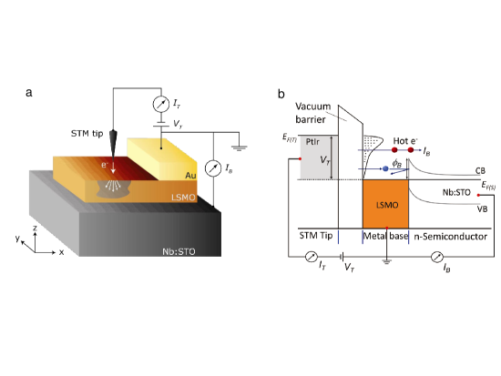
We use a current-perpendicular-to-plane (CPP) configuration to probe vertical transport of hot electrons in the metallic oxide ferromagnet LSMO, across an epitaxial Schottky interface with Nb:STO, using the versatile technique of BEEMbeem . In addition to providing direct quantification of the energy dependent hot electron attenuation length, such a study using BEEM also enables us to analyse nanoscale spatial inhomogeneity of the transport in buried layers with high lateral resolutionvonkanel1 . For these studies, we use 0.01 wt. Nb:STO (001) substrates and deposit LSMO of variable thickness. The devices were fabricated by pulsed laser deposition using TiO2-terminated Nb:SrTiO3 (001) substrates (Nb = 0.01 wt. ). A single unit cell of SrMnO3 was first grown to enhance the Schottky Barrier Height and suppress reverse bias leakage HikitaPRBSBH , and subsequently LSMO films were grown at the O2 partial pressure of 10-1 Torr, substrate temperature of 850∘ C, and at a laser fluence of 0.8 J/cm2. The deposited layer thicknesses were controlled by using reflection high-energy electron diffraction intensity oscillations. For Ohmic contacts, gold was evaporated onto the LSMO, and indium was ultrasonically soldered onto the Nb:STO. In BEEM, a three-terminal transistor configuration, the top LSMO surface is grounded and a negative voltage, VT, is applied to the Scanning Tunneling Microscope (STM) tip, with the tunnel current, IT, kept constant using feedback (Fig. 1). A modified commercial Ultra High Vaccuum (UHV) STM system from RHK Technology was used for the BEEM studies and the measurements were performed at 300 K using PtIr metal tips. The maximum kinetic energy of the electrons injected from the STM tip is given by the applied bias eVT with respect to the metal and transport in the device is thus by hot electrons. No additional bias is applied at the interface between the film and the substrate. After injection and transport through the LSMO thin film, the transmitted electrons are collected in the conduction band of Nb:STO using a third electrical contact. Only those electrons that retain sufficient energy and proper momentum to cross the LSMO/Nb:STO Schottky interface are collectedRippard ; Tamalika Graphite ; Tamalika PRL . Hence the BEEM current, IB, is sensitive to scattering processes and gives important insights into the role of electron correlations to IB during transport.
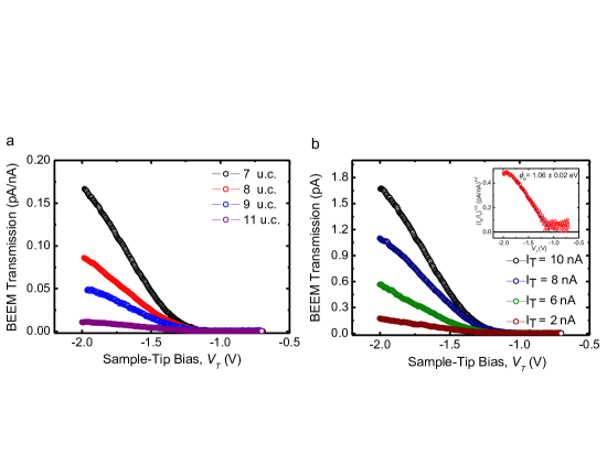
A typical IB-VT curve for hot electron transmission in LSMO at room temperature (RT) is shown in Fig. 2. BEEM transmissions were recorded for four thicknesses of LSMO from 7 to 11 u.c. at different IT (Fig. 2a). Each BEEM spectra represents an average of at least 50 individual IB spectra, measured by positioning the STM tip at several different regions of the film. Approximately four devices of each thickness were measured. IB is observed to decrease with increasing thickness of LSMO. The transfer ratio of the collected current to the injected current (IB/IT) at -2 V for the 7 u.c. LSMO is 0.17 10-3, and reduces to 0.01 10-3 for the 11 u.c. LSMO. For all cases the sign of the current corresponds to electrons flowing from LSMO to Nb:STO and into the ohmic contact. An onset of IB is observed at around 1.06 0.02 eV, which thereafter increases with increasing sample-tip bias . This corresponds to the local Schottky barrier height () extracted using the Bell-Kaiser modelbeem , by plotting the square root of IB with sample-tip bias, VT, as shown in the inset of Fig. 2b. A homogeneous distribution of the local in all devices is obtained which compares well with that obtained from macroscopic I-V, C-V and IPE measurements (see the Supplementary Information). We also observed an almost linear trend in IB with the injected tunnel current, IT, as shown in Fig. 2b, in accord with BEEM theory invoking planar tunnelingLudekeBauer .
The collected BEEM current depends not only on the tunneling current injected into LSMO but also on the energy and momentum distribution of the carriers reaching the interface and the transmission probability at the LSMO/Nb:STO interface. Inelastic scattering, such as due to electron-electron interactions, can reduce the energy of the injected electron by 50 %, whereas elastic scattering from impurities and defects or quasielastic scattering from acoustic phonons render the electron distribution isotropic. The epitaxial LSMO/Nb:STO interfaces studied here have been optimized to be fully strained, atomically abrupt, and with high crystalline perfectionFittingK . Thus they have fewer elastic scattering sites than the typical polycrystalline metal Schottky interfaces studied by BEEM, implying the conservation of transverse momentum of the transmitted electrons across the interface and with minimal influence on IB. IB also depends on the acceptance angle for electron collection at the Nb:STO interface which is determined by the ratio of the effective masses of the Nb:STO and LSMO. This is calculated to be larger here than found for most standard M-S interfaces (such as Au on Si). Availability of allowed states in the conduction band minima (CBM) in space in Nb:STO is another criterion that further governs collection. Electronic band structure calculationsSTO Band structure show that the projected conduction band minima in doped STO are at the zone center (), thus electrons with small parallel momenta should be easily collected in the available phase space. Despite these favourable conditions, a central observation of this first application of BEEM to epitaxial perovskite heterostructures is the strong attenuation observed here, as compared to the highly disordered M-S structures previously studied by this technique. By way of comparison, IB/IT is almost 2 orders of magnitude higher for a similarly thick polycrystalline Ni film on a n-Si/Au M-S interface SubirPRB2012 . Thus we conclude that intrinsic correlation effects are dominant in the measurement.
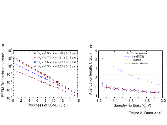
From the data in Fig. 2, we can extract the hot electron attenuation length, , in LSMO and study its energy dependence. For electron transmission in LSMO, is obtained from , where is the sample-tip bias and t is the thickness of LSMO. From Fig. 3a, we find in LSMO to be 1.48 0.10 u.c. at -1.9 V and increases to 2.02 0.16 u.c. at -1.3 V. Using Matthiessen’s rule, the hot electron attenuation length, , can be written as the sum of elastic and inelastic scattering lengths as:
| (1) |
As argued above, elastic scattering is minimal at such epitaxial heterostructures and is thus dominated by . The energy dependence of in LSMO is shown in Fig. 3b.
Discussions
Optimally doped LSMO is a ferromagnet and a transport half-metal with an insulating gap for minority spins at the Fermi level, , and conducting for majority spinsParkNature . However, at energies higher than and relevant for our studies, the density of states for both the majority and minority spin electrons increasesPickettSingh1 ; PickettSingh2 . Conduction and ferromagnetism in LSMO is governed by the interaction of localized electrons from the incomplete shell in Mn, by a process commonly referred to as the Zener double-exchange mechanismZener . Furthermore, as suggested by neutron scattering experimentsChen , LSMO at room temperature consists of dynamic nanoscale polarons, which do not freeze out below the Curie temperature (as opposed to the situation in La0.7Ca0.3MnO3). LSMO separates into regions where the electrons are trapped in a local Jahn-Teller distortion, and a conductive network without distortionsLouca . The transport then occurs as the hot electrons move through the conductive network, while being scattered by the local Jahn-Teller distortions, in addition to the electron-electron scattering of the injected charges themselves. Here, the polaron scattering can be regarded as static because the time scale of lattice motion (picoseconds) is much larger than that of hot electron transport through the LSMO film (femtoseconds)Matsuzaki .
We show that both mechanisms are present in our experiments in Fig. 3b. First, we have attempted a Fermi-liquid theory fit based on the density of states (DOS) previously reported. However, the experimentally determined scattering rate decreases slower than that predicted by this model. Incorporating an energy-independent fitting parameter that accounts for the polaronic scattering processes, we can fit our experimental data by the solid red curve () in Fig. 3b. The obtained fitting constants are well within the ranges expected based on estimates of the band masses and DOS from density functional theory PickettSingh2 . The mean free path due to just the polaronic scattering is expected to be on the order of the polaron separation (or the polaron size). A previous study with neutron measurements estimated this value to be 2 u.c. (0.77 nm)Chen which is roughly consistent with the constant value obtained here. Thus, the hot electron energy dependence enables us to quantitatively isolate two different scattering mechanisms: electron-electron (blue dotted curve) and polaronic scattering (green dotted line).
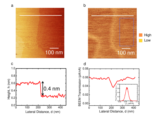
Further, using the imaging capabilities in BEEM we visualize local hot-electron transport across a Nb:STO/LSMO heterointerface. STM topography of the LSMO (9 u.c.)/Nb:STO interface alongwith simultaneously recorded spatial map of the transmitted current, at VT = -2.5 V and IT = 8 nA are shown in Fig. 4. An atomically flat singly terminated TiO2 surface with a step-height of 0.4 nm is observed from the STM topography whereas, a cross-section profile in the same location reveals different transmission at the terrace and at the step-edge with IT being constant. A histogram of the transmitted current at the terrace (area under the blue box in b) is shown in the inset in d. The mean value of IB matches well with that of the BEEM spectra for this film (Fig. 2). The reduction in IB at the step-edge as compared to that at the terrace arises due to the sensitivity of the propagating hot electrons to momentum scattering at the step-edges. This broadens the hot electron distribution and concomitantly reduces IB at such locations. This observation highlights the unique capability of the BEEM to study and directly visualize local electron transport in oxide heterointerfaces at the nanoscale.
Our experimental method, based on hot electron transport in a vertical device structure of LSMO on Nb:STO, provides a first experimental measure of the hot electron attenuation length in a strongly correlated transition metal oxide as LSMO. This approach to probe electron transport, on the nanoscale, will open up exciting possibilities to both understand and tailor the electronic properties at oxide heterointerfaces and advance this emerging field of oxide electronics.
Methods
The devices were fabricated by pulsed laser deposition using TiO2-terminated Nb:SrTiO3 (001) substrates (Nb = 0.01 wt. ). An SrMnO3 single unit cell was first grown to enhance the SBH and suppress reverse bias leakage HikitaPRBSBH , and subsequently LSMO films were grown at the O2 partial pressure of 10-1 Torr, the substrate temperature of 850∘ C, and the laser fluence of 0.8 J/cm2. The deposited layer thicknesses were controlled by using reflection high-energy electron diffraction intensity oscillations. For Ohmic contacts, gold was evaporated onto the LSMO, and indium was ultrasonically soldered onto the Nb:STO. A modified commercial STM system from RHK Technology was used for the BEEM studies. All the BEEM measurements were performed at 300 K using PtIr metal tips, in the constant current mode.
A Pt wire was used to ground the top metal contact. Indium solder defined the Ohmic contact.
Typically 10 devices were fabricated for each thickness. Each BEEM spectra represents
an average of at least 50 individual IB spectra, measured by positioning the STM
tip at several different regions of the film. Approximately four devices of each thickness were measured. The BEEM current is detected with a two-stage amplifier (1011 V/A).
References
- (1) Hwang, H. Y., Iwasa, Y., Kawasaki, M., Keimer, B., Nagaosa, N., & Tokura, Y. Emergent phenomena at oxide interfaces. Nature Mater. 11, 103-113 (2012).
- (2) Choi, T., Lee, S., Choi, Y. J., Kiryukhin, V. & Cheong, S.-W. Switchable ferroelectric diode and photovoltaic effect in BiFeO3. Science 324, 63-66 (2009).
- (3) Yang, S. Y. et al. Above-bandgap voltages from ferroelectric photovoltaic devices. Nature Nanotech. 5, 143-147 (2010).
- (4) Yajima, T., Hikita, Y. & Hwang, H. Y. A heteroepitaxial perovskite metal-base transistor. Nature Mater. 10, 198-201 (2011).
- (5) Garcia, V., Fusil, S., Bouzehouane, K., Enouz-Vedrenne, S., Mathur, N. D., Barthélémy, A., & Bibes, M. Giant tunnel electroresistance for non-destructive readout of ferroelectric states. Nature 460, 81-84 (2009).
- (6) Maksymovych, P., Jesse, S., Ramesh, R., Baddorf, A. P., & Kalinin, S. V. Polarization control of electron tunneling into ferroelectric surfaces. Science 324, 1421-1425 (2009).
- (7) Aeschlimann, M., Bauer, M., Pawlik, S., Weber, W., Burgermeister, R., Oberli, D., & Siegmann, H. Ultrafast spin-dependent electron dynamics in fcc Co. Phys. Rev. Lett. 79, 5158-5161 (1997).
- (8) Monsma, D. J., Vlutters, R., & Lodder, J. C. Room temperature-operating spin-valve transistors formed by vacuum bonding. Science 281, 407-409 (1998).
- (9) Sankey, J. C., Cui, Y-T., Sun, J. Z., Slonczewski, J. C., Buhrman, R. A., & Ralph, D. C. Measurement of the spin-transfer-torque vector in magnetic tunnel junctions. Nature Phys. 4, 67-71 (2008).
- (10) Appelbaum, I., Huang, B., & Monsma, D. J. Electronic measurement and control of spin transport in silicon. Nature 447, 295-298 (2007).
- (11) Gabor, N. M., Song, J. C. W., Ma, Q., Nair, N. L., Taychatanapat, T., Watanabe, K., Taniguchi, T., Levitov, L. S., & Jarillo-Herrero, P. Hot carrier-assisted intrinsic photoresponse in Graphene. Science 334, 648-652 (2011).
- (12) Kaiser, W. J., & Bell, L. D. Direct investigation of subsurface interface electronic structure by Ballistic-Electron-Emission Microscopy. Phys. Rev. Lett. 60, 1406-1409 (1988).
- (13) Hikita, Y. and Hwang, H. Y. “Complex Oxide Schottky Junctions” in Thin Film Metal-Oxide Fundamental and Applications in Electronics and Energy, ed. S. Ramanathan, Springer 2010.
- (14) Meyer, T., & von Känel, H. Study of interfacial point defects by Ballistic Electron Emission Microscopy. Phys. Rev. Lett. 78, 3133-3136 (1997).
- (15) Hikita, Y., Nishikawa, M., Yajima, T., & Hwang, H. Y. Termination control of the interface dipole in La0.7Sr0.3MnO3/Nb:SrTiO3 (001) Schottky junctions. Phys. Rev. B 79, 073101 (2009).
- (16) Rippard, W. H., & Buhrman, R. A. Ballistic electron magnetic microscopy: Imaging magnetic domains with nanometer resolution. Appl. Phys. Lett. 75, 1001-1003 (1999).
- (17) Banerjee, T., van der Wiel, W. G., & Jansen, R. Spin injection and perpendicular spin transport in graphite nanostructures. Phys. Rev. B 81, 214409 (2010).
- (18) Banerjee, T., Haq, E., Siekman, M. H., Lodder, J. C., & Jansen, R. Spin filtering of hot holes in a metallic Ferromagnet. Phys. Rev. Lett. 94, 027204 (2005).
- (19) Ludeke, R., & Bauer, A. Hot electron scattering processes in metal films and at metal-semiconductor interfaces. Phys. Rev. Lett. 71, 1760-1763 (1993).
- (20) Fitting Kourkoutis, L., Song, J. H., Hwang, H. Y., & Muller, D. A. Microscopic origins for stabilizing room-temperature ferromagnetism in ultrathin manganite layers. Proc. Natl. Acad. Sci. U.S.A. 107, 11682-11685 (2010).
- (21) Mattheiss, L. F. Energy Bands for KNiF3, SrTiO3, KMoO3, and KTaO3. Phys. Rev. B 6, 4718-4740 (1972).
- (22) Parui, S., Rana, K. G., Bignardi, L., Rudolf, P., van Wees, B. J., & Banerjee, T. Comparison of hot-electron transmission in ferromagnetic Ni on epitaxial and polycrystalline Schottky interfaces. Phys. Rev. B 85, 235416 (2012).
- (23) Park, J. -H., Vescovo, E., Kim, H. -J., Kwon, C., Ramesh, R., & Venkatesan, T. Direct evidence for a half-metallic ferromagnet. Nature 392, 794-796 (1998).
- (24) Pickett, W. E., & Singh, D. J. Chemical disorder and charge transport in ferromagnetic manganites.Phys. Rev. B 55, R8642-R8645 (1997).
- (25) Pickett, W. E., & Singh, D. J. Electronic structure and half-metallic transport in the La1-xCaxMnO3 system. Phys. Rev. B 53, 1146-1160 (1996).
- (26) Zener, C. Interaction between the d-Shells in the transistion metals. II ferromagnetic compounds of manganese with perovskite structure. Phys. Rev. 82, 403-405 (1951).
- (27) Chen, Y., Ueland, B. G., Lynn, J. W., Bychkov, G. L., & Barilo, S. N. Polaron formation in the optimally doped ferromagnetic manganites La0.7Ca0.3MnO3 and La0.7Ba0.3MnO3. Phys. Rev. B 78, 212301 (2008).
- (28) Louca, D., & Egami, T. Local lattice distortions in La1-xSrxMnO3 studied by pulsed neutron scattering. Phys. Rev. B 59, 6193-6204 (1999).
- (29) Matsuzaki, H., Uemura, H., Matsubara, M., Kimura, T., Tokura, Y., & Okamoto, H. Detecting charge and lattice dynamics in photoinduced charge-order melting in perovskite-type manganites using a 30-femtosecond time resolution. Phys. Rev. B 79, 235131 (2009).
Acknowledgements
We acknowledge financial support from the NWO-VIDI program and the NanoNed program coordinated by the Dutch Ministry of Economic Affairs (K.G.R, S.P & T.B) and thank R. Ruiter for help with an illustration. We acknowledge support from the Department of Energy, Office of Basic Energy Sciences, Division of Materials Sciences and Engineering, under contract DE-AC02-76SF00515 (T.Y., A.F.K., T.P.D., Y.H., & H.Y.H.). T.Y. also acknowledges support from the Japan Society for the Promotion of Science (JSPS).
Authors contributions
T.Y. performed the device fabrication, the current-voltage, capacitance-voltage measurements, and the internal photoemission spectroscopy. K.G.R. performed all the BEEM measurements along with S.P. and contributed to the analysis of the data ; theoretical fits to the extracted data were performed by A.F.K. and T.P.D. Y.H. and H.Y.H. assisted with the planning and the measurements. T.B. conceived and supervised the research and contributed to the analysis of the data. All co authors extensively discussed the results and provided important insights. T.B. wrote the manuscript with input from all co authors.
Additional Information
Supplementary Information accompanies this paper at http://www.nature.com/scientificreports
The authors declare no competing financial interest.