e-mail: llokot@gmail.com
OPTICAL POLARIZATION ANISOTROPY, INTRINSIC
STARK EFFECT AND
COULOMB EFFECTS
ON THE LASING CHARACTERISTICS
OF
[0001]-ORIENTED GaN/Al0.3Ga0.7N
QUANTUM WELLS
Abstract
We present a theoretical investigation of space separated electron and hole distributions, which consists in the self-consistent solving of the Schrödinger equations for electrons and holes and the Poisson equation. The results are illustrated for theGaN/Al0.3Ga0.7N quantum well. The optical gain spectrum in a [0001]-oriented GaN/Al0.3Ga0.7N quantum well in the ultraviolet region is calculated. It is found that both the matrix elements of optical transitions from the heavy hole band and the optical gain spectrum have only the strict (or ) light polarization. We present studies of the influence of the confinement of wave functions on the optical gain which implicitly depends on the built-in electric field calculated to be 2.3 MV/cm. Whereas the structures with narrow well widths exhibit the usual development of the light gain maximum almost without shifting the spectral region, a significant blueshift of the gain maximum is found with increase in the plasma density for wider quantum wells. This blueshift is ascribed to the interplay between the screening of a strain-induced piezoelectric field and the bandstructure. A large Sommerfeld or Coulomb enhancement is present in the quantum well.
1 Introduction
Direct wide band gap group III-nitride semiconductors based on GaN and its alloys have received a great attention due to their applications in optoelectronic devices such as light-emitting diodes and lasers at green-blue and near-ultraviolet wavelengths and solar-blind photodetectors [1, 2]. A number of ultraviolet light-emitting diodes [3, 4, 5, 6, 7, 8] and laser diodes [9, 10, 11, 12, 13] already have been demonstrated. Realizing the deep-ultraviolet semiconductor-based light-emitting diodes will provide compact high-efficiency light sources for various applications, for example to the biological detection and data storage [3]. Thus, these structures are in the developmental stage.
Here, we present a theoretical investigation of the intricate interaction of the electron-hole plasma with a built-in electric field. For this purpose, the calculation of a quantum well bandstructure is performed using the invariant method and the envelope approximation. We consider a quantum well of width in GaN, which is oriented perpendicularly to the growth direction (0001) and localized in the spatial region . In the GaN/AlGaN quantum well structure, there is a strain-induced electric field. This piezoelectric field, which is perpendicular to the quantum well plane (i.e., in z direction) may be appreciable because of the large piezoelectric constants in würtzite structures.
The confinement of wave functions has a strong influence on the optical gain which is observed with an implicit dependence on the built-in electric field which is calculated to be 2.3 MV/cm. Such fields are present in GaN/Al0.3Ga0.7N systems, because the strain is induced by the lattice mismatch. The relative magnitude of piezoelectric effects depends sensitively on the quantum-well width and the plasma density. In this paper, we present the results of theoretical studies of the space separation of electron and hole distributions on the basis of the self-consistent solution of the Schrödinger equations for electrons and holes and the Poisson equation. The Poisson equation contains the Hartree potential which involves the space distributions of the charge density for electrons and holes. We focus on details of the bandstructure for the sake of comparison of different quantum well structures. In the calculations of a band structure in the high-concentration regime, we discuss the treatment of the quantum confined Stark effect (QCSE). By comparing the gain spectra for two GaN/AlGaN quantum well structures with different well widths, we show the interaction of the bandstructure and the piezoelectric field. In particular, we will show that the wide-quantum-well structures, where the QCSE is appreciable, demonstrate a significant blueshift of the gain maximum, whereas the structures with a narrow well width exhibit the ordinary behavior of the light gain maximum almost without shifting the spectral region.
A similar blueshift of the exciton resonance was observed and analyzed on the microscopic level for GaInN/GaN quantum-well systems [14]. They reflect a perturbation of the compensation between the self-energy and the field renormalization contribution to the microscopic interband polarization caused by a real spatial distribution of charges. Such a feature is characteristic of this quantum well and is not inherent to the GaAs quantum well die to the lacking of a piezoelectric field. Accounting the Coulomb renormalization of matrix elements of the electric dipole moment in the two-band model of quantum well structure causes a variation in the oscillator strength with a variation of the carrier density and the quantum well configuration.
In work [15], the matrix elements of the dipole moment for interband transitions and the optical gain of a deformed würtzite GaN quantum well were presented without consideration of the intrinsic built-in piezoelectric field in the quantum well structure.
In work [16], the laser gain was investigated for AlGaN würtzite quantum well structures. The optical gain spectrum was computed by simultaneously diagonalizing the Hamiltonian and by solving the Poisson equation. However, no significant shift of the gain maximum with increase in the plasma density in the framework of single structure was obtained. This indicates that, in the given structure in the high-density regime, QCSE is insignificant. This result coincides with our calculations of the gain shown in Fig. 5.
In work [17], a self-consistent calculation of the optical gain in pseudomorphically strained GaN quantum wells as a function of the carrier density was presented. But the spectrum renormalization and the electric dipole momentum which are caused by electron-electron and electron-hole Coulomb correlations were not considered there.
Understanding the influence of the bandstructure and QCSE on laser gain properties should help one to improve the laser performance and the optimal configurations of a device.
The light gain spectrum presented in the paper reflects only the strict TE (x or y) light polarization. It is known [18, 19, 20, 21, 22] that the valence-band spectrum at the point originates from the sixfold degenerate state. Under the action of the hexagonal crystal field and the spin-orbit interaction in würtzite crystals, splits and leads to the formation of three spin degenerate levels: , upper , and lower levels.
In Section 2 for the processes of emission or absorption, we will calculate the energies and the wave functions of the lowest conduction subband and the valence subbands. The dependences of the matrix elements for dipole optical interband transitions and the light gain spectrum in GaN quantum wells on the quantum well width and the charge density are derived. Section 3 presents the Hartree–Fock light gain spectra and the matrix elements for dipole optical interband transitions that are calculated within the theory described in Section 2. By comparing the light gain spectra for two GaN/AlGaN quantum well structures of different well widths, we show the interaction of the bandstructure, polarization field, and charge density. We determined the red renormalization of the light gain spectrum caused by the electron-electron and hole-hole Coulomb interactions. It is found that the Sommerfeld enhancement composes 26.7 gain value, which was obtained in the Hartree problem. This enhancement of the electric dipole momentum is caused by the electron-hole Coulomb attraction.
2 Theory
We consider QCSE in strained würtzite GaN/Al0.3Ga0.7N quantum wells with widths 2.6 nm and 3.9 nm, in which the barrier height is a constant value for electrons and is equal to meV. The theoretical analysis of the optical gain of strained würtzite quantum well lasers is based on the self-consistent solution of the Schrödinger equations for electrons and holes in quantum well of width with including Stark effect and the Poisson equation. The Poisson equation contains the Hartree potential which involves the charge density for electrons and holes. All researches are performed at a temperature of 300 K.
The first energy level of an electron in the quantum well of width is equal to [23]
| (1) |
where is an electron effective mass, and is determined from equation
| (2) |
where , , and . For the following equality holds:
| (3) |
The wave function of an electron on the first energy level with regard for QCSE is as follows [24]:
| (4) |
Here,
| (5) |
where , , . From the boundary conditions [23, 24] , , , , we find , , , , where is the area of a quantum well in the plane, is the two-dimensional vector in the plane, and is an in-plane wave vector. The constant multiplier is found from the normalization condition
| (6) |
Such a representation of the wave function gives the information that the conduction band corresponds to the representation, which arises due to the splitting of the space group by the crystal field with In other words, the conduction band wave functions originate from atomic orbitals. This is important at the derivation of matrix elements of the electric dipole moment by the Wigner–Eckart theorem.
The strong mismatch of the lattices in GaN and Al0.3Ga0.7N leads to internal strains in the GaN layer. In noncentrosymmetric structures, the internal strains can induce a macroscopic built-in polarization field. This phenomenon is known as the piezoelectric effect. This phenomenon can also be described as a strain inducing an electric field. It is known that this piezoelectric field, which is perpendicular to the quantum well plane, can be significant because of the large piezoelectric constants in würtzite structures which are connected with one another:
| (7) |
where is the piezotensor, is the spontaneous polarization, is the strain tensor, and are the elastic constants, and is the permittivity of the host material. We calculated the built-in piezoelectric field in the GaN/Al0.3Ga0.7N quantum well structure from relation (7) and found V/cm.
We take [25, 17, 26] the following values for constants: GPa, GPa, V/cm, V/cm, V/cm. The transverse components of the biaxial strain are proportional to the difference between the lattice constants of materials of the well and the barrier and depend on the Al content: , , ; nm, nm. The longitudinal component of a deformation is expressed through elastic constants and the transverse component of a deformation: .
One can find the functional, which is built from (4) and (5), in the form
| (8) |
where
| (9) |
,
| (10) |
, and [30]. The quantity can be represented in the form
| (11) |
To account the piezoelectric effects, we modify the Schrödinger equation for electrons and holes, by including an off-diagonal contribution to the electron-hole Hamiltonian. The Schrödinger equation for an infinitely deep quantum well with regard for the QCSE and the Hartree potential created by spatially separated electrons and holes can be presented in the form
| (12) |
where . We introduce the Bloch function written as a vector in the three-dimensional Bloch space:
| (13) |
where
| (14) |
and . The Bloch vector of the -type hole with spin and momentum is specified by its three coordinates in the basis . The envelope -dependent part of the quantum well eigenfunctions can be determined from the boundary conditions for an infinitely deep quantum well as
| (15) |
where is a natural number. The hole wave function can be written as
| (16) |
where in the envelope-wave approximation, in which the wave function is considered as a product of the envelope part and a periodic Bloch multiplier. The Bloch vectors in the envelope wave approximation are projections of the exact Bloch vector on the subspace of vectors with the symmetry inherent to the point [27]. We have
| (17) |
in the basis [28], where
The valence subband structure can be determined by solving the system of equations
| (18) |
where . In the quasicubic approximation, the parameters of effective mass and deformation potential are connected by the relation [19, 21]:
| (19) |
In calculations, we take the effective-mass parameters for the valence band [29] as the parameters for deformation potential [30] as and the energy parameters at 300 K [25, 15] as Solving the Poisson equation
| (20) |
with the condition and with the selected wave functions, we find the Hartree potential :
| (21) |
where , and correspond to the degeneration of the hole band and the first quantized conduction band, respectively, is the value of electron charge, is the permittivity of the host material, and , are the Fermi–Dirac distributions for holes and electrons. Here we assume the charge concentrations , and .
Solving (12) for holes in the infinitely deep quantum well and finding the minimum of functional (8) for electrons in a quantum well with barriers of finite height, we can find the energy and the wave functions of electrons and holes with regard for the space distribution of electron and hole charge densities in the quantum well with given concentrations in a piezoelectric field. The screening field is determined by iterating Eqs. (8), (12), and (21) until the convergence of bandstructure calculations is reached. We use the space carrier distribution of carriers in the lowest order for the envelopes of the wave functions of electrons and holes.
Consider the matrix elements of interband transitions:
| (22) |
The wave functions of the valence band transform according to the the representation , while the wave function of the conduction band transforms according to the representation . In order to find the representation for , let us consider the direct product . The symmetry elements of the point group are as follows:
| (23) |
where is the axis of the -th order, and are 6 planes of reflection which pass through the sixth-order axis. For these elements, we find the representation :
| (24) |
The squares of irreducible representation elements are
| (25) |
We need to find
| (26) |
whereas
| (27) |
The symmetric representation can be found in the form
| (28) |
The antisymmetric representations are
| (29) |
The symmetric representation can be decomposed into the irreducible representations , whereas the antisymmetric one into . Thus, the würtzite Hamiltonian must include the even functions (with respect to the time inversion), which are transformed according to and odd functions, which are transformed according to [19].
The vector representation can be written as
| (30) |
and can be decomposed into the irreducible representations . The representation, according to which the interband operator is transformed, can be decomposed into
| (31) |
Thus, the direct product of representations (31) reflects the existence of nonzero matrix elements of the electric dipole moment of interband transitions, because the vector representation can be formed from these representations.
Allowed matrix elements of the electric dipole moment are found in the form
| (32) |
Due to the symmetry properties of the Bloch functions, the only nonzero matrix elements between the basis functions are [23, 21]
| (33) |
where . Two constants of the matrix elements of the moment are as follows: and . Due to the cylindrical symmetry, the matrix element depends only on the difference between the plane-projected angles of the vectors and k. To simplify calculations, we assume and denote the spherical angles of the vector e by and [21]. We consider the case of a hole wave vector parallel to the axis. In this situation, in our calculations, and the vector e in the spherical coordinates takes the form , whereas . It is known [21] that the values of constants can be found from the kp theory:
| (34) |
From the value of experimentally measured conduction-band effective mass and eV, we obtain eV.
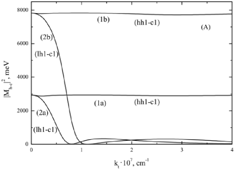
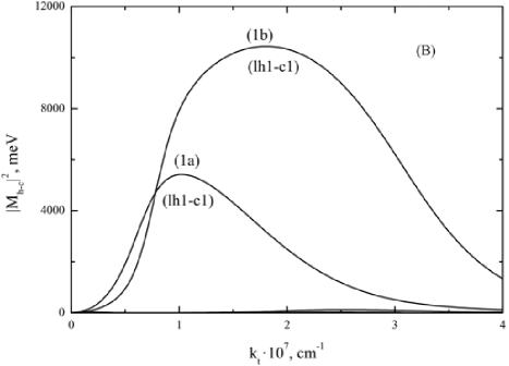
In Fig. 3, we show the -dependence of the matrix elements for the quantum well. We see that the matrix elements have the strict (or ) light polarization for the transitions from the heavy hole band to the conduction band, while for the light polarization, these transitions are forbidden [32]. That is why the light gain spectra presented in Figs. 4 and 5 reflect only the gain of TE polarized light for two widths of the quantum well. Such a behavior agrees with the results of calculations of the moment matrix elements for a würtzite GaN quantum well, since the valence band top originates from , , and irreducible representations. The results which are presented in Figs. 3–5, testify to the optical polarization anisotropy of the matrix elements of the electric dipole moment for interband transitions in GaN/Al0.3Ga0.7N quantum well structures.
The optical gain of a material [31, 15] can be calculated from the Fermi golden rule
| (35) |
where is the magnitude of electron charge, is the electron rest mass in the free space, is the velocity of light in the free space, is the permittivity of the host material, and are the Fermi–Dirac distributions for electrons in the conduction and valence bands, respectively, e is a unit vector of the vector potential of the electromagnetic field, is the interband energy of the conduction and valence bands, is the optical energy, and is a half-linewidth of the Lorentzian function, which is equal 6.56 meV. We consider the electromagnetic wave which propagates in the plane of the quantum well. The modal gain, which determines the threshold condition of a laser, is proportional to the material gain multiplied by the optical confinement factor and by the number of quantum wells in the case of multiple quantum wells: . We take equal to 0.01, and is taken to be 1 in the calculations.
Although the carriers within each band are in a strongly nonequilibrium state, the interband relaxation times are much larger than intraband relaxation times. Therefore, the Fermi–Dirac statistics can be used in the calculations.
Using the expressions for the basis functions, we obtain two scalar polarizations for the matrix elements of the electric dipole moment. For the TE-polarization ( or axis), i.e., for the light polarization vector lying in the quantum well plane, we have
| (36) |
For the TM-polarization ( axis), i.e., for the light polarization vector, which is perpendicular to the quantum well plane, we have
| (37) |
3 Results and Their Discussion
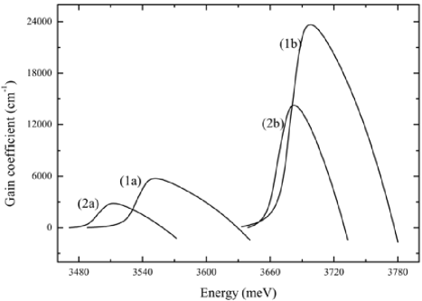
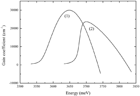
To describe the interplay of the bandstructure and the polarization effects in the Hartree problem, we consider the 2.6-nm and 3.9-nm GaN/Al0.3Ga0.7N quantum well structures. In the quantum well 2.6 nm in width at a concentration of , a optical gain maximum is equal to at the wavelength nm; while, at a concentration of , the optical gain maximum is equal to . Such a gain is observed at the wavelength nm. In the quantum well 3.9 nm in width at a concentration of , the optical gain maximum is equal to at the wavelength nm; while, at a concentration of , the optical gain maximum is equal to . Such a gain is calculated at the wavelength nm. Thus, the optical gain in the GaN/Al0.3Ga0.7N quantum well develops in the ultraviolet spectral region, as shown in Fig. 4.
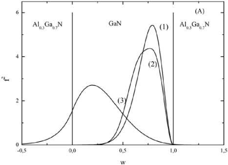
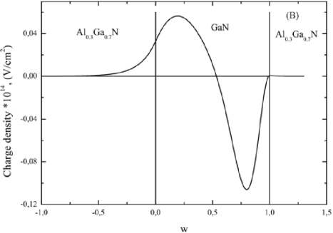
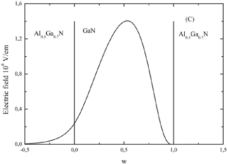
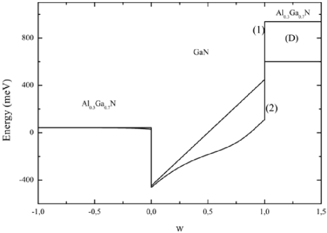
Numerically solving the Schrödinger equations (8) and (12) for electrons and holes and the Poisson equation (20), the steady state solutions allow us to construct the squares of the wave functions of a heavy hole (1), a light hole (2) (e.g., at the transverse wave vector ), and an electron (3) (A); the charge density distribution on the quantum well width (B); the effective screening electric field distribution (C); and the quantum well potential and the screening potential on the quantum well width (D). The results of calculations for the concentration for a 3.9-nm quantum well are shown in Figs. 1 and 2, and the Hartree gain spectra are presented in Fig. 4. For the narrow quantum well, we see that, at a density of the light gain is gradually developed, as the carrier density increases. At high densities (i.e., when the density is equal to ), the optical gain develops nearly in the spectral region of the original optical gain at a plasma density of .
The behavior of the light gain coefficient for two quantum well widths and at given concentrations can be understood from Figs. 1(A,B) and 2(C,D). From Fig. 1(A), we see that the overlap between the quantum confined electron and hole wave functions is related to the charge density distribution over the quantum well width, which is shown in Fig. 1(B). We can conclude that, for the wide quantum well, the overlapping integral is smaller than that for a narrow quantum well and reduces stronger with decrease in the carrier density.
The effective screening electric field distribution for wide-bandgap GaN/AlGaN quantum well systems, which is presented in Fig. 2(C), is similar to that of the electric field in a condenser.
As shown in Fig. 4, the situation is quite different for the 3.9-nm GaN/Al0.3Ga0.7N quantum well structure. Because of a weaker quantum confinement in this relatively wide quantum well, the piezoelectric field is able to significantly reduce the overlap between the quantum confined electron and hole wave functions, which can be seen from the comparison of Figs. 1 and 2. As a result the interband dipole matrix element or the oscillator strength is substantially smaller than that in the case for the narrow 2.6-nm quantum well. This intrinsic quantum confined Stark effect can also cause a significant redshift of the gain maximum at a plasma density of as compare with the flat-bottom band situation. As the plasma density increases, the screening of the QCSE increases the overlap of electron-hole wave functions and, hence, the exciton oscillator strength. Simultaneously, the weakened piezoelectric field, which induced earlier the redshift, leads to the net of blueshifts in the gain maximum and the absorption edge with increase in the plasma density, as shown in Fig. 4.
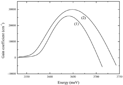
To calculate the concentration dependence of many-body Coulomb effects in the absorption spectrum of a GaN quantum well, we apply the method developed in [33, 14, 34]. Numerically solving the microscopic polarization equation, we see that, with increase in the plasma density, the optical gain (i.e., negative absorption) develops in the spectral region of the original exciton resonance. With increase in the free-carrier density, the ionization continuum shifts rapidly to the long-wavelength side, whereas the 1s-exciton absorption line stays almost constant, due to a high degree of compensation between the weakening of the electron-hole binding energy and the band-gap reduction, like that earlier found for GaAs [35]. At high electron-hole concentrations, the electric dipole moment renormalization effects give rise to a large optical gain which is shown in Figs. 5 and 6. The maximum of the Hartree–Fock gain spectrum equal to is observed at the wavelength nm at a concentration of . From Fig. 6, we see that the Hartree–Fock spectrum is shifted to the long-wavelength side relative to the Hartree gain spectrum. Moreover, a large Sommelfeld or Coulomb enhancement is present in the quantum well. It is caused by an increase of the oscillator strength due to the electron-hole Coulomb attraction.
The exchange Hartree–Fock energy spectrum renormalization is accounted in the equation of motion for the microscopic dipole of the electron-hole pair. For high concentrations, this value is significant. It is somewhat larger for electrons and less for holes. Totally, this value is reflected in the Hartree–Fock gain shifting in comparison with the Hartree spectrum, as shown in Fig. 6. It should be noted that the gain spectrum involves not only Hartree–Fock correlations, but correlations of higher orders in the expansion in the Coulomb potential energy. This is achieved by the summation of the series in the Coulomb energy in the microscopic polarization equation in all orders of perturbation theory. In more details, the microscopic polarization equation for the dipole of an electron-hole pair for the würtzite quantum well will be considered in our next paper.
4 Conclusions
In summary, the self-consistant calculations of the Schrödinger equations and the Poisson equation of wide bandgap GaN/AlGaN quantum well systems show the interesting dependences of the matrix elements for dipole optical interband transitions and the light gain spectrum on the quantum well width and the charge density. A blueshift with increase in the plasma density in the gain spectrum in relatively wide wells occurs as a consequence of the screening of the piezoelectric field induced by the quantum confined Stark effect, whereas the structures with narrow well widths exhibit the usual dependence of the development of the light gain maximum almost without shifting the spectral region. It is found that the matrix elements of optical transitions from the heavy hole band have the strict TE light polarization like that of the light gain spectrum. With regard for the Coulomb interactioin, a red shift of the Hartree–Fock light gain spectrum relative to the Hartree gain spectrum and a large Sommerfeld enhancement for a quantum well are found.
The author is grateful to Prof. V.I. Sheka and Prof. V.A. Kochelap for numerous discussions.
References
- [1] S. Nakamura and G. Fasol, The Blue Laser Diode (Springer, Berlin, 1997); R.L. Aggarwal, P.A. Maki, Z.-L. Liau, and I. Melngailis, J. Appl. Phys. 79, 2148 (1996); S. Nakamura, M. Senoh, S. Nagahama, N. Iwasa, T. Yamada, T. Matsushita, H. Kiyoku, and Y. Sugimoto, Jpn. J. Appl. Phys. 1 35, L74 (1996); S. Nakamura, J. Vac. Sci. Technol. A 13, 705 (1995).
- [2] N. Savage, Nature Photonics 1, 83 (2007).
- [3] A. Khan, K. Balakrishnan, and T. Katona, Nature Photonics 2, 77 (2008).
- [4] Y. Taniyasu, M. Kasu, and T. Makimoto, Nature Lett. 441, 325 (2006).
- [5] A.H. Mueller, M.A. Petruska, M. Achermann, D.J. Werder, E.A. Akhadov, D.D. Koleske, M.A. Hoffbauer, and V.I. Klimov, NanoLetters 5, 1039 (2005).
- [6] T. Wang, S. Wu, K.B. Lee, J. Bai, P.J. Parbrook, R.J. Airey, Q. Wang, G. Hill, F. Ranalli, and A.G. Gullis, Appl. Phys. Lett. 89, 081126 (2006).
- [7] B.F. Chu-Kung, M. Feng, G. Walter, N. Holonyak, jr., T. Chung, J. -H. Ryou, J. Limb, D. Yoo, S.-C. Shen, R.D. Dupuis, D. Keogh, and P.M. Asbeck, Appl. Phys. Lett. 89, 082108 (2006).
- [8] H. Hirayama, J. Appl. Phys. 97, 091101 (2005).
- [9] T. Asano, M. Takeya, T. Mizuno, S. Ikeda, K.K. Shibuya, T. Hino, S. Uchida, and M. Ikeda, Appl. Phys. Lett. 80, 3497 (2002).
- [10] S.-N. Lee, S.Y. Cho, H.Y. Ryu, J.K. Son, H.S. Paek, T. Jang, K.K. Choi, K.H. Ha, M.H. Yang, O.H. Nam, Y. Park, and E. Yoon, Appl. Phys. Lett. 88, 111101 (2006).
- [11] L.L. Gaddard, S.R. Bank, M.A. Wistey, H.B. Yuen, Z. Rao, and J.S. Harris, jr., J. Appl. Phys. 97, 083101 (2005).
- [12] E. Feltin, D. Simeonov, J.-F. Carlin, R. Butte, and N. Grandjean, Appl. Phys. Lett. 90, 021905 (2007).
- [13] H. Yoshida, Y. Yamashita, M. Kuwabara, and H. Kan, Nature Photonics 2, 551 (2008).
- [14] W. Chow, M. Kira, and S.W. Koch, Phys. Rev. B 60, 1947 (1999).
- [15] S.L. Chuang, J. Quantum Electron. 32, 1791 (1996).
- [16] W.W. Chow and M. Kneissl, J. Appl. Phys. 98, 114502 (2005).
- [17] J. Wang, J.B. Jeon, Yu.M. Sirenko, and K.W. Kim, Photon. Techn. Lett. 9, 728 (1997).
- [18] E.I. Rashba, Sov. Phys. Solid State 1, 368 (1959); E.I. Rashba and V.I. Sheka, ibid, 162 (1959); G.E. Pikus, Sov. Phys. JETP 14, 898 (1962).
- [19] G.L. Bir and G.E. Pikus, Symmetry and Strain-Induced Effects in Semiconductors (Wiley, New York, 1974).
- [20] P.Y. Yu and M. Cardona, Fundamentals of Semiconductors (Springer, Berlin, 1996).
- [21] Yu.M. Sirenko, J.-B. Jeon, K.W. Kim, M.A. Littlejohn, and M.A. Stroscio, Phys. Rev. B 53, 1997 (1996).
- [22] R.G. Banal, M. Funato, and Y. Kawakami, Phys. Rev. B 79, 121308(R) (2009).
- [23] L.D. Landau and E.M. Lifshitz, Quantum Mechanics (Pergamon Press, Oxford, 1977).
- [24] G. Bastard, E.E. Mendez, L.L. Chang, and L. Esaki, Phys. Rev. B 28, 3241 (1983).
- [25] I. Vurgaftman, J.R. Meyer, and L.R. Ram-Mohan, J. Appl. Phys. 89, 5815 (2001).
- [26] Semiconductors, edited by O. Madelung (Springer, Berlin, 1991); W. Shan, T.J. Schmidt, X.H. Yang, S.J. Hwang, J.J. Song, and B. Goldenberg, Appl. Phys. Lett. 66, 985 (1995).
- [27] Yu.M. Sirenko, J.-B. Jeon, B.C. Lee, K.W. Kim, M.A. Littlejohn, M.A. Stroscio, and G.I. Iafrate, Phys. Rev. B 55, 4360 (1997).
- [28] S.L. Chuang and C.S. Chang, Phys. Rev. B 54, 2491 (1996).
- [29] M. Suzuki, T. Uenoyama, and A. Yanase, Phys. Rev. B 52, 8132 (1995).
- [30] S.L. Chuang, C.S. Chang, and A. Yanase, Phys. Rev. B 54, 2491 (1996).
- [31] V.V. Mitin, V.A. Kochelap, and M.A. Stroscio, Quantum Heterostructures (Cambridge Univ. Press, New York, 1999).
- [32] L.O. Lokot, Semicon. Phys. Quantum Electron. Optoelectron. 11, 364 (2008); L.O. Lokot, Ukr. Fiz. Zh. 54, 964 (2009).
- [33] M. Lindberg and S.W. Koch, Phys. Rev. B 38, 3342 (1988).
- [34] W.W. Chow, S.W. Koch, and M. Sargent III, Semiconductor Laser Physics (Springer, New York, 1994).
-
[35]
H. Haug and S. Schmitt-Rink, Prog. Quant. Electr. 9, 3
(1984).
Received 11.04.2011
ОПТИЧНА ПОЛЯРИЗАЦIЙНА АНIЗОТРОПIЯ,
ВНУТРIШНIЙ ЕФЕКТ ШТАРКА
КВАНТОВОГО
КОНФАЙНМЕНТУ I ВПЛИВ КУЛОНIВСЬКИХ
ЕФЕКТIВ НА ЛАЗЕРНI
ХАРАКТЕРИСТИКИ
-ОРIЄНТОВАНИХ GaN/Al0,3Ga0,7N
КВАНТОВИХ ЯМ
Л.O. Локоть
Р е з ю м е
У цiй статтi представлено теоретичне
дослiдження просторово роздiлених електронних i дiркових
розподiлiв, яке вiдображається у самоузгодженому
розв’язаннi рiвнянь Шредiнгера для електронiв та дiрок i рiвняння
Пуассона. Результати проiлюстровано для
GaN/Al0,3Ga0,7N квантової ями. Спектр оптичного
пiдсилення в [0001]-орiєнтованої GaN/Al0,3Ga0,7N
квантової ями обчислено в ультрафiолетовiй областi. Знайдено, що як
матричнi елементи оптичних переходiв з важкої дiркової пiдзони в
зону провiдностi, так i спектр оптичного пiдсилення мають строго
x (або y) поляризацiю свiтла. Показано вплив
конфайнменту хвильових функцiй на оптичне пiдсилення, яке
неявно залежить вiд вбудованого електричного поля, що обчислене i
дорiвнює 2,3 MВ/cм. Якщо структури з вузькою шириною ями проявляють
звичайну залежнiсть розвитку максимуму пiдсилення свiтла
майже без змiщення спектральної областi, то значного голубого
змiщення максимуму пiдсилення зi зростанням густини плазми
набувають структури зi значною шириною квантової ями. Це голубе
змiщення вiдносять до взаємодiї мiж екрануючим п’єзоелектричним
полем, створеним деформацiєю i зонною структурою. Велике
зоммерфельдiвське або кулонiвське пiдсилення присутнє у
квантовiй ямi.