Ultra-high-ohmic microstripline resistors for Coulomb blockade devices
Abstract
In this paper, we report on the fabrication and the low-temperature characterization of extremely high-ohmic microstrip resistors made of a thin film of weakly oxidized titanium. Nearly linear voltage-current characteristics were measured at temperatures down to for films with sheet resistivity up to as high as , i.e. about an order of magnitude higher than our previous findings for weakly oxidized Cr. Our analysis indicates that such an improvement can help to create an advantageous high-impedance environment for different Coulomb blockade devices. Further properties of the Ti film addressed in this work show a promise of low-noise behavior of the resistors when applied in different realizations of the quantum standard of current.
1 Introduction
Experimental observation and electronic applications of quantum tunneling phenomena, in many cases, put forward the requirement of efficient decoupling of the tunneling system from the environmental degrees of freedom responsible for dissipation [1, 2]. This implies, for the practical devices, that low noise operation should be possible for the tunneling systems embedded into the DC biasing circuitry with an effective output impedance far exceeding the resistance quantum up to the frequency and energy ranges relevant for the particular transport mechanisms [3, 4, 5].
For a mesoscopic tunneling system, one of the possibilities of constructing a high-ohmic bias is to co-fabricate it on-chip with an adjoining microstrip of a high-resistivity thin-film material. For example, successful realizations of quantized charge transport have been demonstrated in ultrasmall tunnel junctions, see, e.g., Refs. [6, 7, 8, 9, 10], and superconducting nanowires (as quantum phase slip junctions) [11] with the help of a few micrometer-long weakly oxidized Cr resistors of a typical cross-section (thickness linewidth) with the resistances per unit length up to . A detailed analysis, see, e.g., Ref. [12], and the experimental data obtained so far [8, 9, 11] indicate, however, a significant shunting effect due to the stray capacitances of the microstrip, typically [12], so that for the frequencies exceeding the roll-off value
| (1) |
the on-chip resistor of a certain length and a designated impedance must be considered as a distributed RC line rather than as a simple lumped element (see, e.g., Ref. [2]). In the high-frequency limit, the impedance of the line decays approximately as a square root of frequency
| (2) |
descending below the resistance quantum , i.e., beyond the high-impedance case, for the frequencies above .
Given the due value of and the value of fixed by the microstripline design, equation 1 demonstrates an important role of the unit length resistance for developing high-ohmic environments effective in a wide frequency range. Unfortunately, fabricating thinner or stronger oxidized Cr resistors often results in irreproducible granular films exhibiting a pronounced Coulomb blockade of a net current at low temperatures [13]. In the present work, we report on resistivity behavior of films of titanium evaporated in the presence of oxygen at low pressure. The choice of Ti is inspired by its relatively high resistivity value, about [14], while its affinity to oxygen can be utilized for avoiding the superconductivity of Ti below the transition temperature , as well as for achieving even higher film resistivity. At low temperature, we demonstrate a linear current-to-voltage dependence for the Ti resistors with being about an order of magnitude higher than the corresponding values for the Cr films, which makes Titanium an attractive material choice for resistively-biased Coulomb blockade devices based on both tunnel- and quantum phase slip junctions.
2 Experiment and Discussion
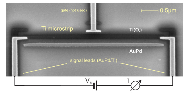
The experimental structures, see Fig. 1, were fabricated using electron-beam lithography and the shadow-evaporation technique [15] which is often implemented for structuring ultrasmall tunnel junctions of Al (see a detailed description of our fabrication routine in Ref. [16]). In this technique, a thin Ti film was first evaporated from the standard e-gun source at a slanted incidence of material onto the substrate, followed by a normal-angle evaporation of a thicker film of AuPd to form well-conducting current leads. Because of the well-pronounced gettering property of Ti films, the important parameters of our process were the base chamber pressure, , and the evaporation rate of Ti . In order to increase film resistivity, the deposition of Ti was performed reactively with a small amount of oxygen gas added to the evaporation chamber at a low pressure . The samples were tested electrically at room temperature on the day of the evaporation, demonstrating a clear monotonous dependence of the resistance on the oxygen pressure, as shown in Fig. 2. We selectively tested a few samples after a month or two of shelf life to find an up to increase in film resistivity due to the prolonged air contact.
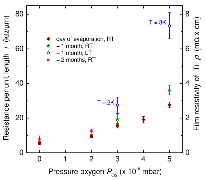
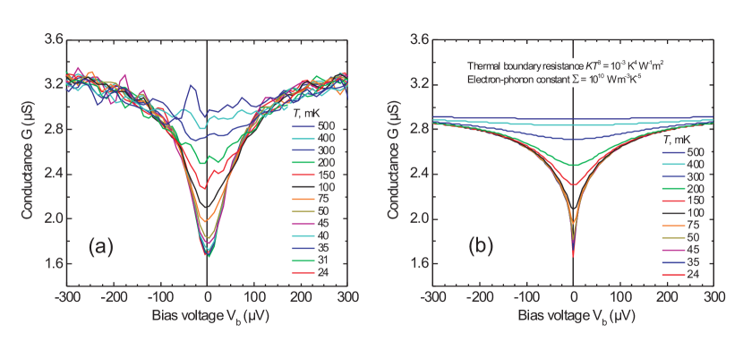
The resistors were characterized in the dilution fridge down to the operating temperatures of the Coulomb blockade devices below . Due to the oxygen content in the Ti film, a negative temperature profile of resistance was observed with the values increasing by the factor 1.5—2 down to a few degrees Kelvin, see Fig. 2. This temperature behavior is consistent with the findings of other groups reported for high-ohmic Ti films, see, e.g., Refs. [17, 18], indicating a strong impurity scattering limit of conductivity electrons in the film. The curves were found to be almost linear for all tested resistors, with a weak nonlinearity around the origin, appearing at the lowest temperatures as a zero-bias conductance dip in Fig. 3(a). Remarkably, the height of the dip, increasing towards lower temperatures, was found to come to saturation at the substrate temperature very close to the base temperature of the fridge. This indicates very efficient thermalization of the conduction electrons on the phonons of the crystal lattice and gives rise to a promise of a very low level () of thermal noise in the mK-temperature range, which is quite favorable for applications in the quantum current standard [3, 5, 7].
For a more detailed understanding of the current transport mechanism, we first address a straightforward hypothesis of a purely thermal origin of the conductance dip, . We take into account the Joule heating effect of current through the Ti resistor and calculate the electron temperature according to the one-fifth power law [19, 20]:
| (3) |
where is the heat flow from the electron gas to the lattice phonons in the Ti microstrip, is the electron-phonon coupling constant, the volume of the resistor, and the phonon (lattice) temperature of the resistor. Here, is the contact area between the microstrip and the substrate. We expect to be close to the substrate temperature due to a typically small value of thermal boundary resistance , namely, [21].
An important simplification of our model was made due to the high resistivity of the Ti film giving rise to a strong scattering approximation for conduction electrons on the crystal lattice. In particular, we assumed a fully local heat dissipation by the electron-phonon interaction mechanism and neglected small energy losses across the boundary Ti/AuPd, so that . Correspondingly, the temperature profile along the microstrip is regarded as being flat except for the sharp temperature drops at both ends of the Ti wire. Further on, at we assumed and used the experimental zero-bias conductance values to establish an empirical calibration relation . From now on, we adopt , being independent of : the approximation is justified in part by an independence of on in Fig. 3(a) for , where is common for all curves, but the values of vary. Finally, the conductance dips were calculated to be shown in Fig. 3(b), using the calibration curve and the values obtained from Eq. 3.
The assumption used for the calibration curve ignores possible additional heating of the sample by the external noise (voltage fluctuations coming through the leads to the Ti microstrip) and supposedly results in the sharper and less noisy dips calculated for the lowest values of in Fig. 3(b). On the other hand, our even simplified model demonstrates a reasonable agreement with the experiment. In this way, it provides a distinct argument for the purely thermal origin of the dip, making less probable a presence of unwanted granular Coulomb blockade effects (cf., e.g., the case of partially oxidized Cr films [13] or the anodized Ti films in Ref. [22]) and related shot-noise effects. An indirect support of this conclusion also appears in the form of a very low noise level measured in the resistor in the frequency range around , typical for the background charge fluctuations phenomena in the single-electron tunneling devices [23]. The noise was found unresolvable against the intrinsic noise level of the current preamplifier.
Due to the higher attainable values of in the Ti, as compared to Cr, and according to Eq. 1, a roll-off frequency higher by one order of magnitude is now expected for the high-ohmic environmental impedance available for applications. For example, for the hybrid single-electron turnstile [4] with typically [24], the roll-off frequency is and the high-impedance behavior extends up to [25], indicating a remarkably wide energy range, up to , where the quantum system is decoupled from the environment, thus making the suppression of Cooper-pair-electron (CPE) cotunneling leakage [4] potentially more efficient. For applications with the Bloch oscillations devices [6, 9] and quantum phase slip junctions [11], a narrowing by an order of magnitude for the linewidth of oscillations, [3] and, therefore, substantial improvement of the shape of Shapiro-like current steps at (under microwave irradiation of frequency , in the limit ) are expected [26].
In conclusion, we report on exceedingly high-ohmic microstripline resistors made of titanium films evaporated reactively in the presence of oxygen. This new material exhibited a sheet resistance of up to which is an order of magnitude higher than that of formerly used Cr films and is expected to be free of intrinsic Coulomb blockade effects related to film granularity even at the lowest temperatures of the experiment. Due to the latter fact, a further increase in resistivity seems to be possible without immediate loss of linearity. The obtained parameters, in particular, a considerable improvement in the roll-off frequency, are promising for the application of Ti resistors in different realizations of quantum standards of current.
Acknowledgements
Stimulating discussions with A. B. Zorin are gratefully acknowledged. Technological support from T.Weimann and V. Rogalya is appreciated.
References
References
- [1] Caldeira A O and Leggett A J 1983 Quantum tunnelling in a dissipative system Annals of Physics 149 374-456
- [2] Ingold G L and Nazarov Yu V 1992 Charge tunneling rates in ultrasmall junctions Single Charge Tunneling, Coulomb Blockade Phenomena in Nanostructures (NATO ASI Series B vol 294)(New York: Plenum Press) ch 2
- [3] Likharev K K and Zorin A B 1985 Theory of the Bloch-wave oscillations in small Josephson junctions J Low Temp Phys 59 347-381
- [4] Pekola J P, Vartiainen J J, Möttönen M, Saira O-P, Meschke M, and Averin D V 2008 Hybrid single-electron transistor as a source of quantized electric current Nature Physics 4 120
- [5] Mooij J E and Nazarov Yu V Quantum phase slip junctions 2006 Nature Phys. 2 169-172
- [6] Kuzmin L S and Haviland D B 1991 Observation of the Bloch oscillations in an ultrasmall Josephson Junction Phys Rev Lett 67 2890-2893
- [7] Lotkhov S V, Bogoslovsky S A, Zorin A B and Niemeyer J 2001 Operation of a three-junction single-electron pump with on-chip resistors Appl Phys Lett 78 946-948
- [8] Lotkhov S V, Krupenin V A, and Zorin A B 2007 Cooper pair transport in a resistor-biased Josephson junction array IEEE Trans Instr Meas 56 491-494
- [9] Maibaum F, Lotkhov S V, and Zorin A B 2011 Towards the observation of phase-locked Bloch oscillations in arrays of small Josephson junctions Phys Rev B 84 174514
- [10] Camarota B, Scherer H, Keller M W, Lotkhov S V, Willenberg G-D, and Ahlers F J 2012 Electron counting capacitance standard with an improved five-junction R-pump Metrologia 49 8-14
- [11] Hongisto T T and Zorin A B 2012 Single-charge transistor based on the charge-phase duality of a superconducting nanowire circuit Phys Rev Lett 108 097001
- [12] Zorin A B, Lotkhov S V, Zangerle H, and Niemeyer J 2000 Coulomb blockade and cotunneling in single electron circuits with on-chip resistors: Towards the implementation of the R-pumpJ Appl Phys 88 2665-2670
- [13] Krupenin V A, Zorin A B, Savvateev M N, Presnov D E, and Niemeyer J 2001 Single-electron transistor with metallic microstrips instead of tunnel junctions J. Appl. Phys. 90 2411
- [14] see, e.g., online: http://www.webelements.com/titanium/physics.html
- [15] Dolan G J 1977 Offset masks for lift-off photoprocessing Appl Phys Lett 31 337-339, Niemeyer J 1974 Eine einfache Methode zur Herstellung kleinster Josephson-Elemente PTB-Mitt 84 251-253
- [16] Lotkhov S V, Camarota B, Scherer H, Weimann T, Hinze P, and Zorin A B 2009 Shunt-protected single-electron tunneling circuits fabricated on a quartz wafer Nanotechnology Materials and Devices Conference, NMDC ’09 IEEE 23 - 26
- [17] Singh R and Surplice N A 1972 The electrical resistivity and resistance-temperature characteristics of thin titanium films Thin Solid Films 10 243-253
- [18] Hofmann K, Spangenberg B, Luysberg, and M Kurz H 2003 Properties of evaporated titanium thin films and their possible application in single electron devices Thin Solid Films 436 168 174
- [19] Roukes M L, Freeman M R, Germain R S, and Richardson R C 1985 Hot electrons and energy transport in metals at millikelvin temperatures Phys Rev Lett 55 422-425
- [20] Wellstood F, C Urbina C, and Clarke J 1994 Hot-electron effects in metals Phys Rev B 49 5942-5955
- [21] Swartz E T and Pohl R O 1989 Thermal boundary resistance Rev Mod Phys 61 605-668
- [22] Johannson J, Schöllmann V, Andersson K, and Haviland D B 2000 Coulomb blockade in anodised titanium nanostructures Physica B 284-288 1796-1797
- [23] Krupenin V A, Presnov D E, Zorin A B, and Niemeyer J 2000 Aluminium single electron transistors with islands isolated from the substrate J. Low Temp. Phys. 118 287-296
- [24] Lotkhov S V, Kemppinen A, Kafanov S, Pekola J P and Zorin A B 2009 Pumping properties of the hybrid single-electron transistor in dissipative environment Appl Phys Lett 95 112507
- [25] This value should however be reduced, if taking into account the tunnel junction capacitances contributing to the total effective impedance of the environment. Still, for the state-of-the-art junctions with typically , this correction will not be critical.
- [26] Likharev K K 1986 Dynamics of Josephson Junctions and Circuits (Gordon and Breach, New York)