Abrupt barrier contribution to the electron spin splitting in asymmetric coupled double quantum wells.
Abstract
We have studied the behavior of the electronic energy spin-splitting of based double quantum wells (narrow gap structures) under in-plane magnetic and transverse electric fields. We have developed an improved version of the Transfer Matrix Approach that consider contributions from abrupt interfaces and external fields when tunneling through central barrier exists. We have included the Landé -factor dependence on the external applied field. Also, we have calculated electron density of states and photoluminescence excitation. Variations of the electron spin-splitting energy lead to marked peculiarities in the density of states. Because the density of states is directly related to photoluminescence excitation, these peculiarities are observable by this technique.
pacs:
72.25.-b, 73.21.-b1. Introduction
In the last decade a great interest has arisen for the so-called spintronic, or spin-based electronics. The reason is that the spintronic, due to its low power consumption, promises to be a good alternative to the traditional electronics, based on the charge transport 1 . On the other hand, the spin transport is not very dissipative, with low energy losses over long distances, although the relaxation of the spin polarization may exist. Spintronics is a catchall term that refers to the potential use of the spin rather than the charge in electronic devices. For it to be useful in practice, spin up and spin down electronic states (or hole states) of any material must be separated in energy. Also, the material should be electrically polarized as in conventional electronics, which means that carriers, both negative (electrons) and positive (holes), must be able to conduct.
A key point is the choice of the material. For example, narrow gap semiconductors with strong spin-orbit coupling. -based materials seem to be the suitable candidates2 due to the long life of the magnetic spin state of photoexcited electrons, which behaves coherently. It is also important that the materials have a good lattice matching to avoid defects accumulation at the interface and internal strains, which would worsen the transport of the polarized spin. There exist techniques to relax this strain, as to place step graded buffers with a progressive variation of the concentration between the substrate and the active device. These layers mainly absorb strain and defects.
Another important point is a large Landé factor for having a significant splitting of spin states by applying small magnetic fields. In general, structure seems to be one of the most appropriate for spintronic purposes. This heterostructure offers the possibility of manipulate the gap width, the Landé factor and the interface contributions by varying and concentrations. Besides, it presents a remarkable spin-splitting energy when a weak magnetic fields is applied. This peculiarity makes this material suitable for high temperature spin-valves devices.
In this work we will focus in the spin-splitting changes in asymmetric coupled double quantum wells ACQW, caused by abrupt interfaces, when an in-plane magnetic field is applied. For this purpose we will base on an extended version of the Kane formalism with nonsymmetric boundary conditions to calculate the band structure and dispersion laws3 . Although electronic dispersion laws (and the corresponding spin-orbit splitting) in quantum heterostructures have been widely studied in the last decades4 , many question remain open. One of them is the influence of heterojunctions on the electron spin tunneling and thus, their contribution to the polarization of this spin. In theory, effects from compositional parameters or interface contributions to the spin splitting should be analyzed through the density of states. And the modifications of the density of states can be directly observed using photoluminescence excitation technique (PLE)5 .
In bulk materials spin-orbit interaction is caused either by a soft potential 6 and by cubic 7 and linear 8 spin-dependent contributions to the effective Hamiltonian. However, in the two-dimensional (2D) case, we can reduce the cubic contribution to a linear one after the squared momentum substitution by its quantized value due to confinement 9 . Moreover, it is necessary to consider the additional spin-orbit splitting caused by the interaction with abrupt heterojunction potentials (see Ref. 1 ; 3 ; 10 ; 11 ). This contribution is absolutely different to the contributions mentioned above.
The effect of an in-plane magnetic field on the energy spectrum in nonsymmetric heterostructures results in the Pauli contribution to the electron Hamiltonian. Several peculiarities for transport phenomena in heterostructures have been also discussed 12 ; 13 ; 14 ; 15 . However, these discussions only consider the mixing between Pauli contribution and effective 2D spin-orbit interaction. As mentioned above, we cannot forget the contribution of the abrupt barriers in asymmetric structures (e.g. ACQW) to the spin splitting, as we will emphasize in this work. Besides, we have included possible changes of the Landé factor. Although the Landé -factor depends on the applied fields 16 ; 17 , this dependence is negligible for in-plane magnetic fields and low electron density. The model also applies to narrow-gap heterostructures whenever the slow potential generated by doping or external transverse electric fields can be described self-consistently.
2. Eigenstate problem
We will center our attention in the Hamiltonian describing the electronic behavior in the conduction band, considering that any possible strain is already included in the structure through the gap, the conduction and the valence well potentials18 . We will include effects of electric and magnetic fields as well as the interfaces contribution.
Based on the assumption that the gap energy is smaller than the energy distance between the valence band (-band) and the spin-split band extrema, the electronic states in these narrow-gap heterostructures can be described by the three-band Kane matrix Hamiltonian
| (1) |
where the generalized kinetic momentum, , contains the vector potential , is an in-plane magnetic field and is written in the -representation through the 2D momentum . We have also introduced the diagonal energy matrix whose elements fix the positions of the band extrema and the interband velocity matrix .
From now on it is necessary to introduce a new index to denote narrow-gap regions (wells) and wide-gap regions (central barrier and lateral sides), respectively. In the parabolic approximation we can write the Schrödinger equation for ACQW in the form3 :
| (2) |
where the isotropic kinetic energy is given by
| (3) |
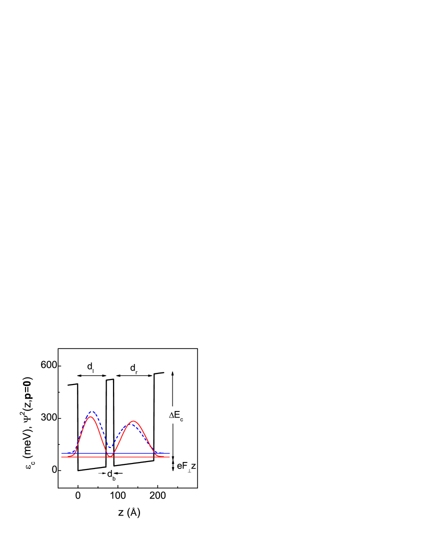
which includes the effective mass . Parabolic approximation is justified because energy values under consideration are smaller than the gap energy in the narrow region. The energy is in the wells, and in the barriers, where is the band offset for conduction band. Whenever energy values are less than underbarrier penetration (and tunneling) is permitted and described by the boundary conditions. The potential , for an uniform transverse electric field, is . Band diagram for ACQW is shown in Fig. 1.
The magnetic energy , for not very strong magnetic fields, is described by
| (4) |
where is the Bohr magneton and is the Pauli matrix. Finally, the characteristic spin velocity , and the effective Landé factor are
| (5) |
The potential of interfaces determines a part of the spin dependent contributions through the parameter . Actually, takes into account the spin-orbit coupling due to the abrupt potential of the heterojunction at each interface, as3 ; 11
| (6) |
where the integral is taken over the width of the abrupt interface . Contribution of to the energy dispersion relations will appear through the third kind boundary conditions after a first integration of the Schrödinger equation (2). We will detail this point in Appendix A.
In the present case, where is linear with , we get , which does not depend on . Thus, the external applied electric field shapes the spin velocity and the -factor, . We can take the characteristic spin velocity for each layer as
| (7) |
and the abrupt interface parameter as
| (8) |
Lastly, we introduce the Pauli splitting energy , caused by the magnetic field, as . Thus, Eq. (4) becomes
| (9) |
which has lost the dependence.
Because and do not depend on , we can factorize fundamental solutions of Eq. (2), , as products of and functions, with . The value refers to the two possible spin orientations. For an ACQW under a transverse electric field , the -dependent spinors can be obtained from
| (10) |
in the form
| (13) | |||||
| (16) |
where
| (17) |
and the energy quasi-paraboloids are
| (18) |
Now, -dependent functions are obtained from the second order differential equation
| (19) |
For an ACQW under a transversal electric field , eigenstate functions of Eq. (14) are the known linear combination of the Airy - and -functions. Thus, the general solution of Eq. (2) can be written as
| (20) | |||||
where are four constants by region to be solved through the interface conditions of continuity of the wave functions and current. Because there are two wells, and three barriers (Fig. 1), there are four interfaces and four boundary conditions by interface.
Next, to simplify the calculation of the wave functions and the dispersion relations of the electronic levels through the boundary conditions3 ; 10 , we create two auxiliary parameters: a length and an energy
| (21) |
and a set of momentum dependent functions
| (22) |
Next, using preliminary quasi parabolic dispersion relations , we construct the Airy function arguments
| (23) |
where acts as a Kronecker function: when , and when .
We use the transfer matrix method to obtain wave functions and energy dispersion relations of the electronic levels. In the present case, we have improved the standard method by using matrices at each interface, whose elements are (see Appendix A):
| (24) |
where means , and the same for
Now we are ready to generate transfer matrices, which elements are Finally, electronic levels for each 2D momentum are obtained from , where
| (25) | |||||
In the above matrix product, denotes interfaces position in the growth direction, starting from the left side.
Calculations give us two spin up and two spin down paraboloids, where corresponds to the deepest coupled levels of the ACQW. Once obtained coefficients (Eq. 15) we normalize wave functions for each momentum .
The scheme of Fig. 1 includes the two resonant energy levels and the respective wave functions for . Although there are four levels only two are observable in this figure. This is because spin sublevel splitting is much smaller than electronic level energy distance and differences between spin down and spin up wave functions are not visible at .
Finally, the density of states can be obtained by using the well-known expression
| (26) |
Peculiarities of can be analyzed experimentally through the photoluminescence excitation (PLE) intensity for the case of near-edge absorption, , because both quantities are related by11
| (27) |
for very low temperature, or
| (28) |
when including electron-phonon scattering. In the above expression, the Gaussian function is . The Gaussian halfwidth is related to the scattering and relaxation processes and, thus, to the temperature19 . Expressions (23, 24) are valid provided the interband velocity does not depend on in-plane momentum. Here is the light polarization vector, , and , are the conduction and valence band levels, respectively.
3. Results
Let’s start this section with numerical results for -based ACQWs, with and . We have chosen this particular structure because we have reliable data for basic parameters20 ; 21 . We have considered two wells of and Å wide separated by a Å barrier. We have also applied an electric field of kV/cm, which corresponds to a spin velocity cm/s for the QWs, and cm/s for the barriers, with a transition spin velocity region across de abrupt interface. This electric field is slightly higher than needed to achieve resonance between the deepest levels of both wells ( kV/cm). To calculate interface contributions we have used a typical abrupt interface size of for 22 . We have also applied in-plane magnetic field of T, small enough to allow the anticrossing close to the bottom of energy dispersion relations (zero slope points).
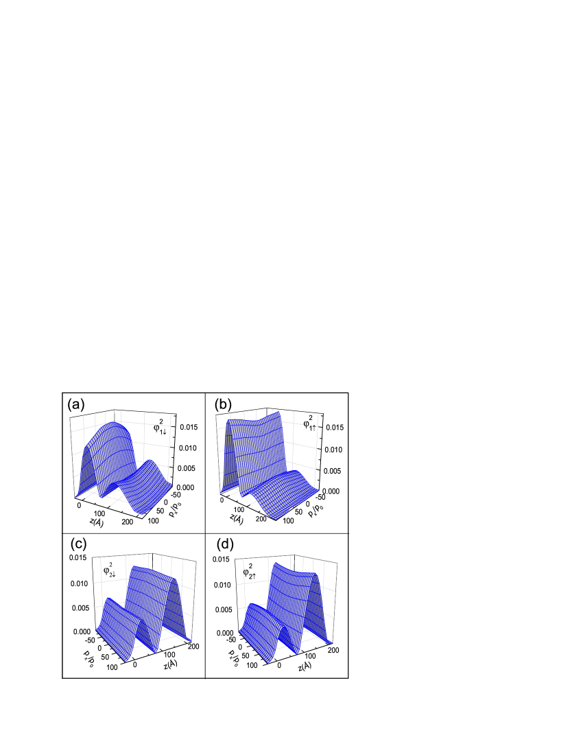
Figures 2 show normalized squared wave function for , versus and the dimensionless momentum , where . Upper panels correspond to the first deepest level for the two different spin orientations. As expected for an electric field beyond the resonance, charge density is mainly located in the left narrow QW. Consequently, the opposed happens for the second resonant level as can be seen in the lower panels Analyzing wave functions versus momentum and spin orientations by comparing panels and , a particular behavior occurs. While the charge distribution coincide for both down and up spins at the zone center (), there is a tunneling charge transfer between wells for increasing . For spin down case [panel ] charge enhances tunneling from left narrow well to the right wide one. Tunneling shows opposite behavior for spin up electrons [panel ()] and charge goes from the right to the left well. Lower panels correspond to the higher resonant level, mainly at the right well. It might seem the behavior is the opposite to the previous one because now, spin down case [panel ] shows a tunneling increase from right to left QW as increases and, conversely, for spin up electrons [panel ]. However, considering the relative charge concentration between wells, we can realize there is a similar behavior for both resonant levels. For spin down electrons there is a charge shift from well with higher concentration to the other well [panels , ] and conversely for the spin up electrons [panels , ]. The reason for this charge shift lies in the magnetic energy term , which induces a breaking of the momentum symmetry. Because of is an essential part of the argument of the Airy functions, the behavior of the wave functions is significantly affected.
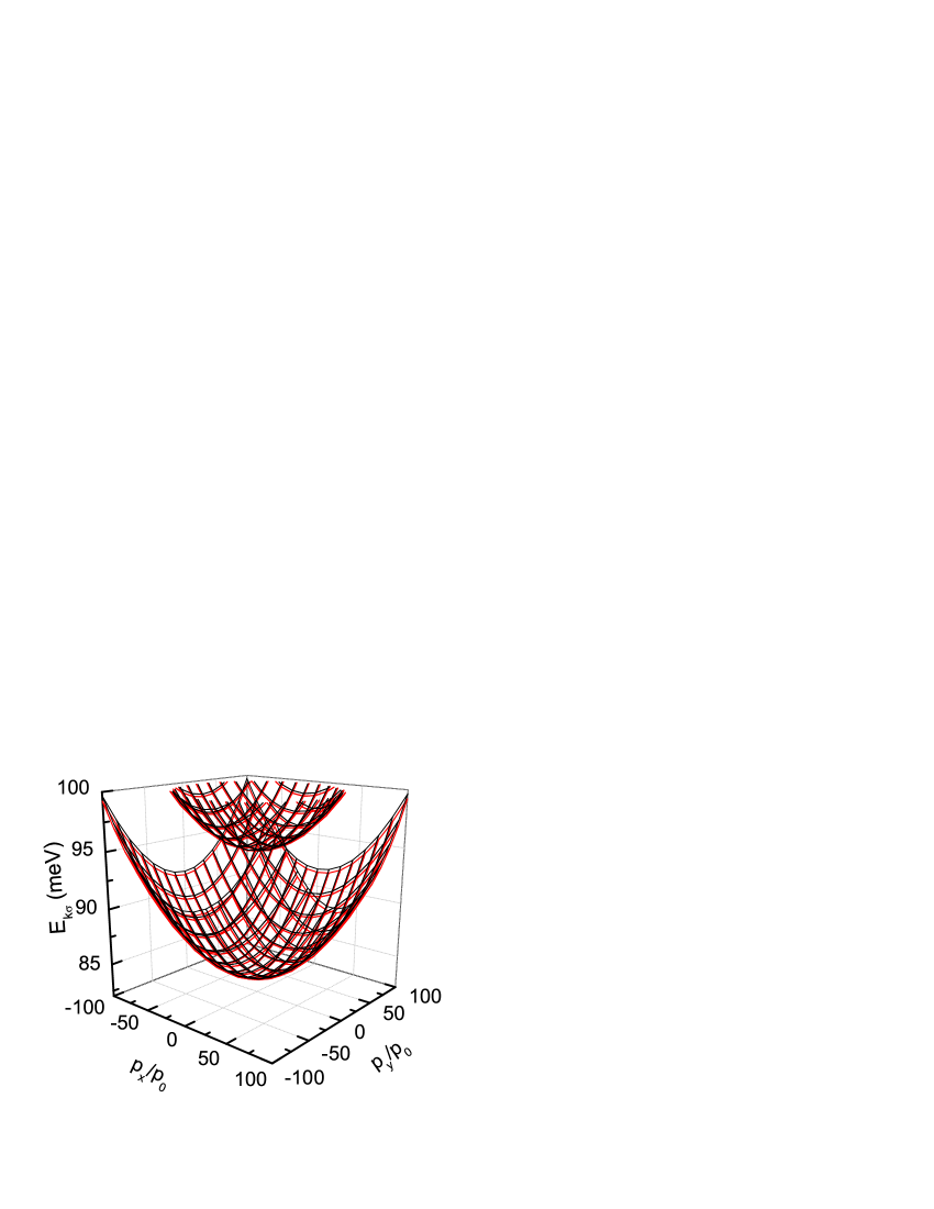
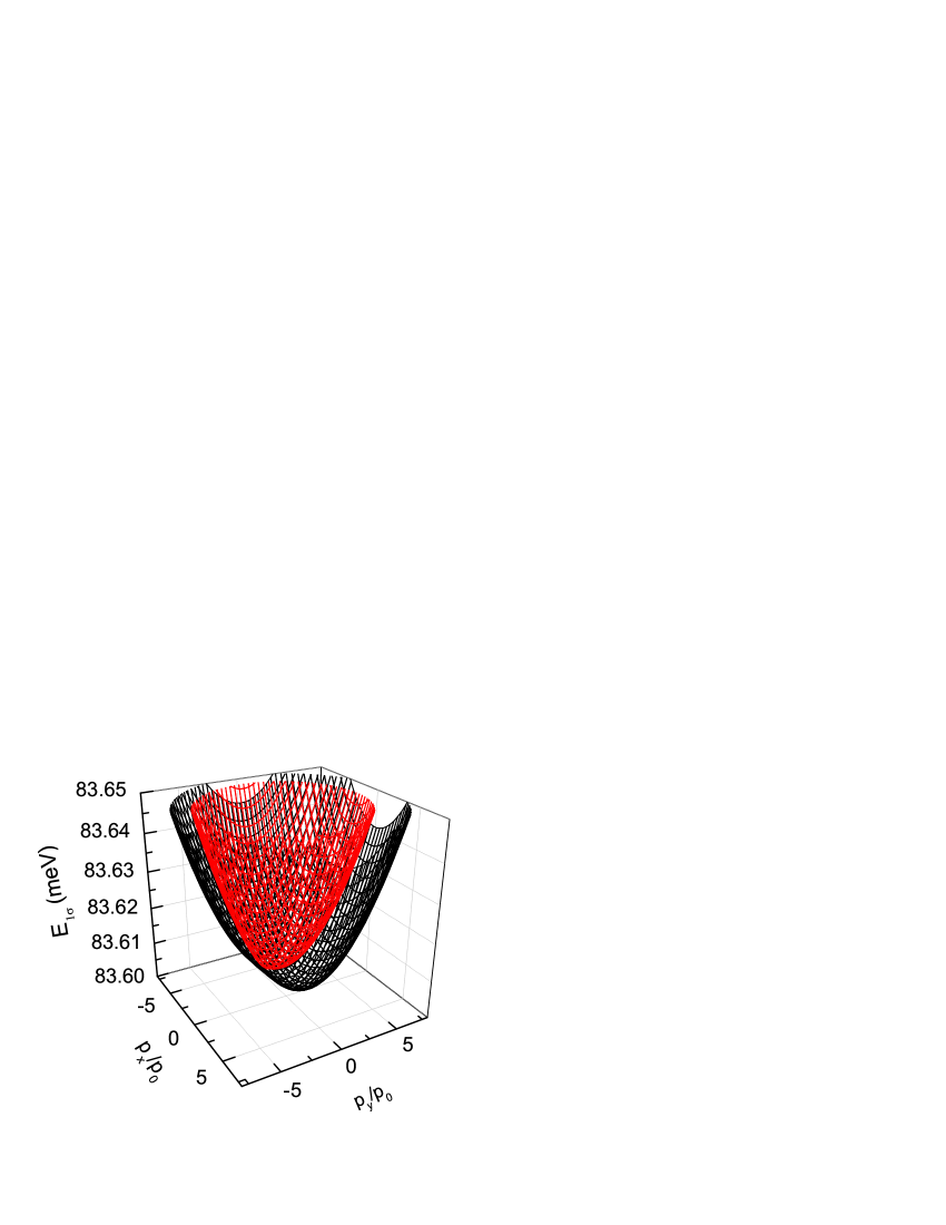
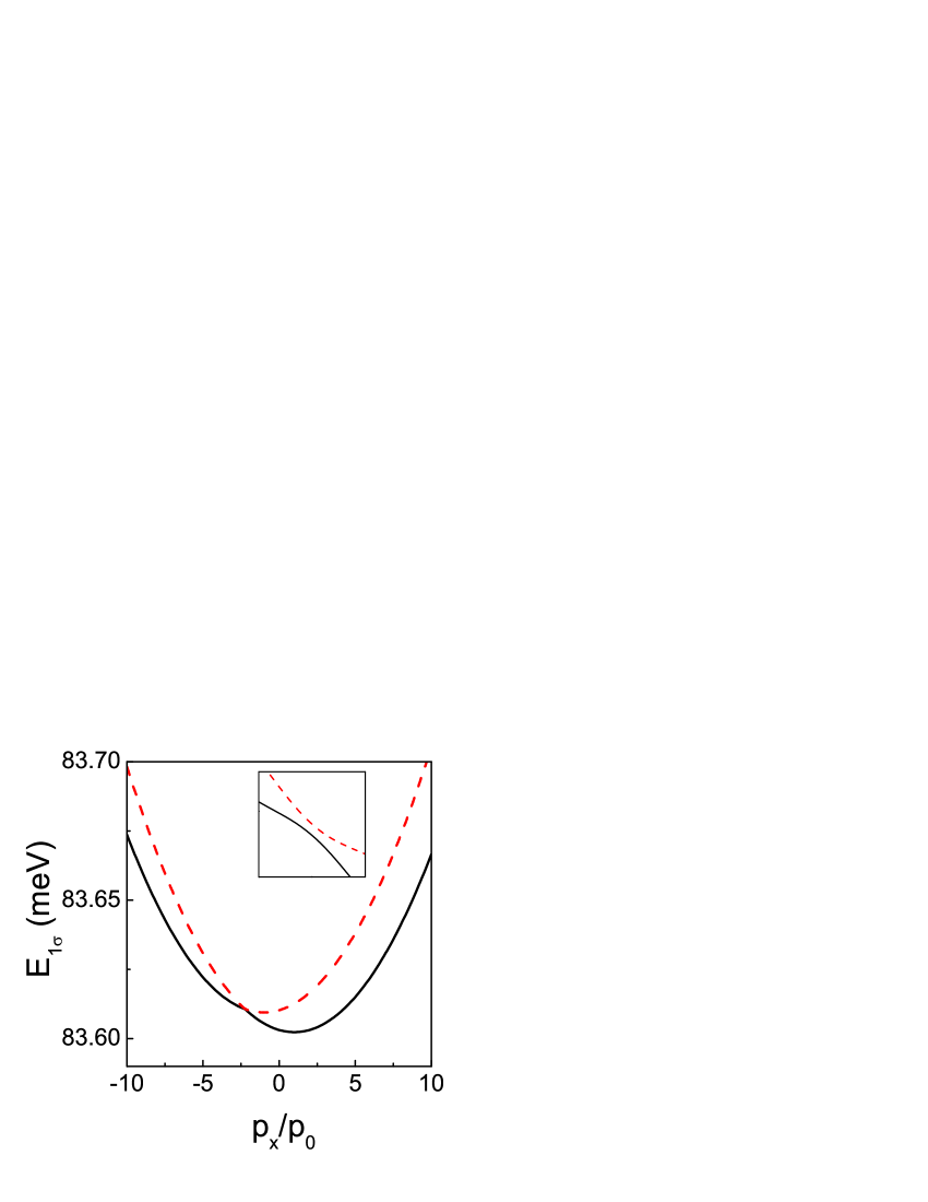
Fig. 3 shows the near parabolic dispersion relations of the two coupled levels and their corresponding spin down and up sublevels, for the electric and magnetic fields under consideration. It can be seen the paraboloids symmetry according to Eqs. (12) and (13). Although there is a little difference between spin paraboloids, due to the large energy difference between the resonant levels of both wells (12 meV) and the splitting of the spin sublevels (0.01 meV at ) it is not possible to distinguish minima behavior. Thus, we have enlarged in Fig. 4 the bottom of the pair of paraboloids (spin down and spin up) for the ground level. As expected, both paraboloids shift in opposite directions resulting in a sublevel anticrossing. This displacement is due not only to the magnetic field but also to the electric one (12).
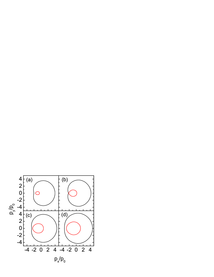
Considering a section of the former figure we can get a more accurate 2D representation (Fig. 5) of the anticrossing, minima position, and energy splitting. The inset displays anticrossing area enlargement. In this kind of anticrossing the slope of varies without changing the sign. However, as we will see below for the low magnetic fields under study, we work in the region where Van Hove singularities remain in the density of states. In order to have a more detailed overview of the anticrossing region we have also included in Fig. 6 the contour plot around anticrossing for different constant energy values.
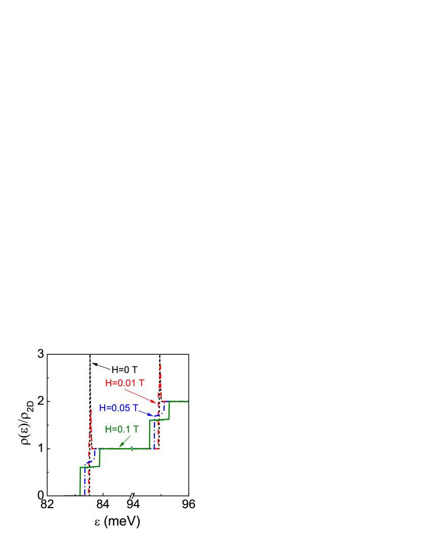
Next, we analyze the density of states . This function is related to several spin and interwell tunneling properties. Also, it is proportional to the photoluminescence excitation (PLE) intensity, one of the most used techniques to get information of quantum structures 23 . As mentioned before, we have found remains of the Van Hove singularities for fields under consideration. So, we have used magnetic field intensities varying from to T to analyze singularities behavior. The shape of is shown in Fig. 7. Note that, when T, energy paraboloids shift a certain amount because of the dependence on the electric field. In this case, because both paraboloids bottom are at the same energy, we have clear type singularities in each subband. As expected, these peaks disappear gradually by growing magnetic field because of the different vertical paraboloids shift, which leads to a greater slope at the anticrossing point. In turn, interfaces contribute with a manifested delay in the quenching of the singularities, as well as an additional broadening of these peaks. That is, although the singularities should only appear at zero magnetic field, they still remain at the band anticrossing position for low magnetic fields, as shown in Fig. 7. Another significant feature is that the anticrossing peak is softened when increasing barrier height, disappearing for lower magnetic fields than used in this work3
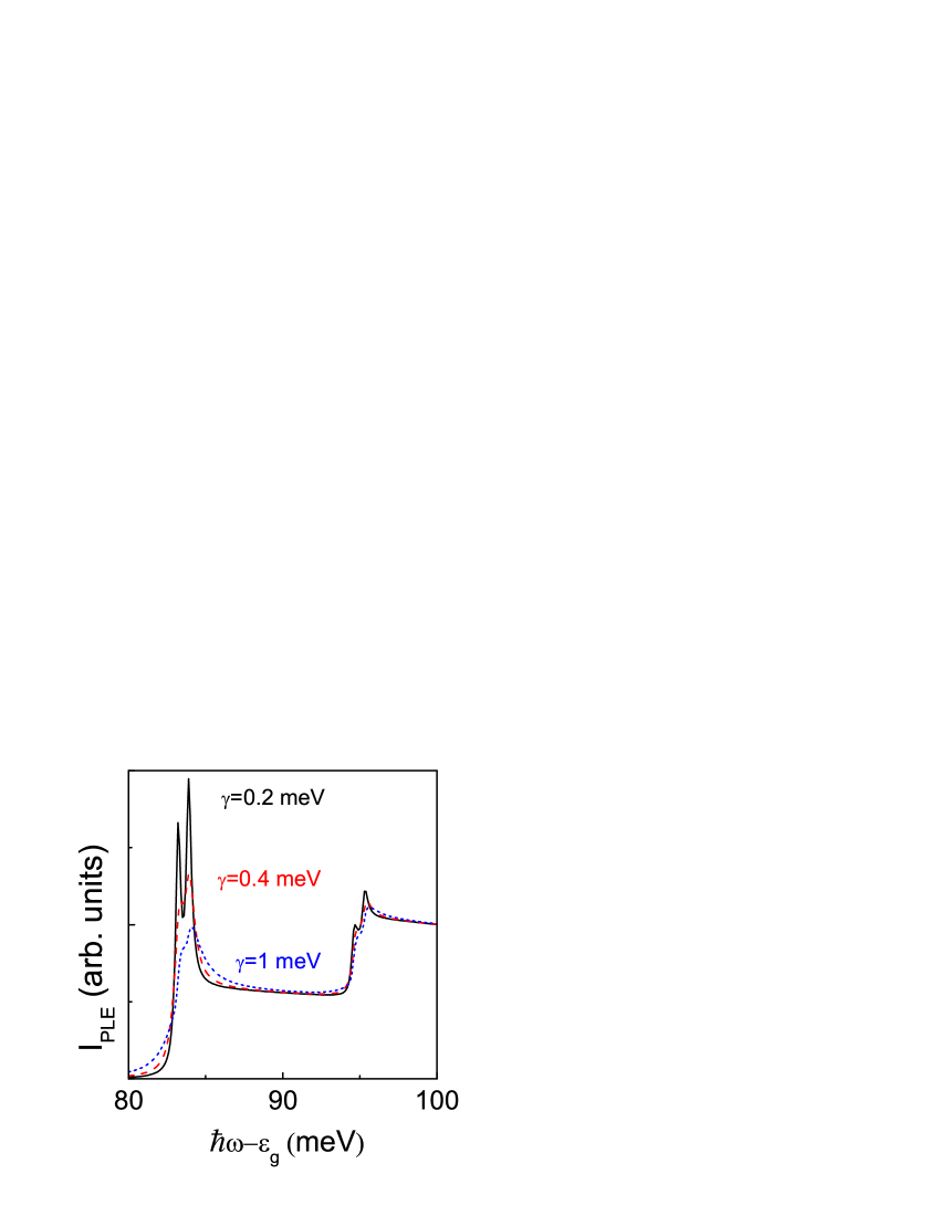
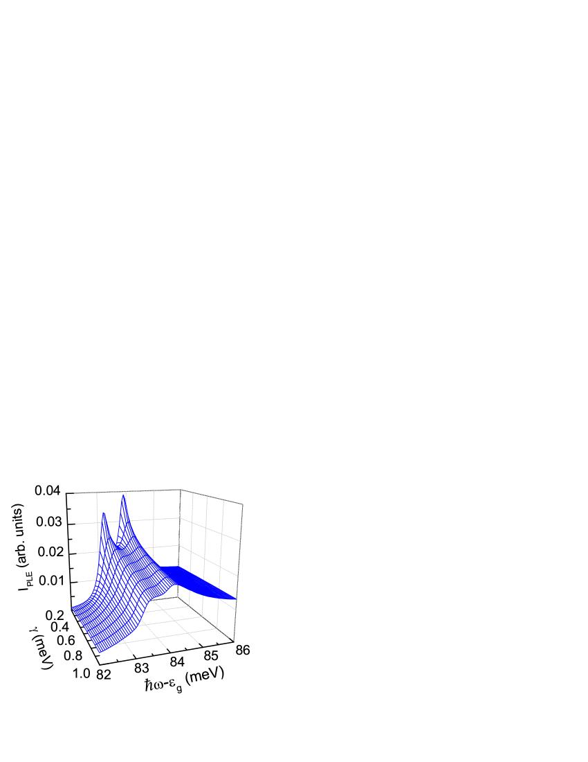
Finally, Fig. 8 shows PLE spectra for different Gaussian halfwidth at a fixed T. For the magnetic field used before ( T) the two adjacent peaks, corresponding to each resonant pair of states, overlap. Thus, we have used a magnetic field ten times higher because this field allows us to tell the peaks apart for small values. Evolution of the first two peaks with is depicted in Fig. 9. As can be seen, PLE peaks corresponding to the two different spin transitions are still distinguishable for values beyond meV. These results show the same general behavior than available experimental data24 .
4. Conclusions
In this paper we have analyzed the electron spin behavior in narrow-gap ACQWs under transverse electric and in-plane magnetic fields, including the role of abrupt interfaces. We used the Kane model with nonsymmetric boundary conditions, caused by the two different wells width, to solve the eigenvalue problem. Based in this model and the transfer matrix approach we have performed a useful tool to tackle any layered structure with abrupt interfaces and subjected to different perturbations. To do that we have implemented matrices for the boundary conditions to describe near-parabolic dispersion relations. The model allows us the study of the spin peculiarities of levels anticrossing.
Because interface contributions oppose intrinsic spin-orbit effect, mechanisms that mix the Pauli contribution with the two kinds of spin-orbit contributions (from a low magnetic field and from heterojunctions) are different. As a result, numerical calculations for structures lead to magnetoinduced variations of the energy dispersion relations, under very low in-plane magnetic fields. This effect is particularly appreciable at anticrossings. As dispersion relations are used to obtain the density of states, this function is also affected by the abrupt interfaces: a new kind of singularity, which does not disappear when increasing magnetic fields, appears. Furthermore, there is an energy broadening of the peaks.
Finally, we have calculated PLE intensity because, as mentioned before, mid-infrared PLE spectroscopy is a suitable technique to find characteristics of energy spectrum23 . This technique provides direct information of the energy spectrum when interband transitions are modified by in-plane magnetic fields.
Since, for our purposes, a thorough analysis of the band structure little contributes to describe eigenstates, the main conclusions of this work remain valid. We have also used along the work the assumption that the confined potential is well described. Thus, the effective transverse field provides correct estimations both for magnetoinduced changes and for the character of the dispersion laws. However, more detailed numerical calculations are needed to describe the kinetic behavior. We will return to this point in a forthcoming work where we will analyze the spin dynamics in ACQWs. In summary, we have shown the importance of the contribution from the interfaces, in narrow gap structures, to the spin polarization through the electronic dispersion relations, and how this contribution can be detected by PLE. The model can be extended to the analysis of the negative magnetoresistance25 as well as peculiarities of the spin current through ADQW26
Appendix A Boundary conditions
After a first integration of the Schrödinger equation over an heterojunction at , we get the third class boundary conditions:
| (29) |
together with the wave function continuity at interfaces
| (30) |
which lead to a set of four equations we can write as
| (33) | |||
| (34) |
After substitution of by in (A3) we obtain:
The matrix form of the above equations for coefficients , leads to expression (20).
References
- (1) B.A. Bernevig and S. Zhang, IBM J. Res. and Dev. 50, 1 (2006).
- (2) J.M. Kikkawa and D.D. Awschalom, Phys. Rev. Lett. 80, 4313 (1998).
- (3) A. Hernández-Cabrera, P. Aceituno, and F. T. Vasko. Journal of Luminescence 128, 862 (2008). A. Hernández-Cabrera, P. Aceituno, and F. T. Vasko, Phys. Rev. B 74, 035330 (2006).
- (4) W. Zawadzki and P. Pfeffer, Semicond. Sci. Technol. 19 R1 (2004).
- (5) S. Nomura and Y. Aoyagi, Surface Sci. 529 171 (2003); F. Giorgis, F. Giuliani, C. F. Pirri, A. Tagliaferro, and E. Tresso, Appl. Phys. Lett. 72 (1998).
- (6) V. F. Gantmakher and I. B. Levinson, Carrier Scattering in Metals and Semiconductors (North-Holland, Amsterdam, 1987).
- (7) G. Dresselhaus, Phys. Rev. 100, 580 (1955).
- (8) E.I. Rashba, Sov Phys. Sol. State 2, 1109 (1960); E.I. Rashba and V.I. Sheka, Sov. Phys. Solid State 3 1718 (1961).
- (9) M.I. Dyakonov, and V.Y. Kachorovskii, Sov. Phys. Semicond. 20 110 (1986).
- (10) F.T. Vasko. JETP Lett.30 360 (1979).
- (11) F.T. Vasko and A.V. Kuznetsov, Electronic States and Optical Transitions in Semiconductor Heterostructures (Springer, New York, 1999).
- (12) P. Pfeffer and W. Zawadzki, Phys. Rev. B 59 R5312, 1999; Y. Lin, T. Koga, and J. Nitta, Phys. Rev. B 71, 045328 (2005).
- (13) B. Das, D.C. Miller, S. Datta, R. Reifenberger, W.P. Hong, P.K. Bhattacharya, J. Singh, and M. Jaffe, Phys. Rev.B 39, R1411 (1989).
- (14) T. Kita, Y. Sato, S. Gozu, and S. Yamada, Physica B 298, 65 (2001).
- (15) A. Hernández-Cabrera, P. Aceituno, and F.T. Vasko, Phys. Rev. B 60, 5698 (1999).
- (16) P.A. Shields, R.J. Nicholas, K. Takashina, N. Grandjean, and J. Massies, Phys. Rev. B 65, 195320 (2002).
- (17) A.A. Kiselev, E.L. Ivchenko, and U. Rössler, Phys. Rev. B 58, 16353 (1998).
- (18) I. Vurgaftman, J.R. Meyer, and L.R. Ram-Mohan, J. Appl. Phys. 89, 5815 (2001).
- (19) A. L. Ivanov, P. B. Littlewood, and H. Haug, Phys. Rev. B 59, 5032 (1999).
- (20) Following Refs. 12-14 and I. Vurgaftman, J.R. Meyer, and L.R. Ram-Mohan, J. Appl. Phys. 89, 5815 (2001), we use the data for structure: , , where is the electron mass, factor , permittivity , meV, meV, and meV.
- (21) A. Stroppa and M. Peressi, Phys. Rev. B 71, 205303 (2005).
- (22) P. Velling, M. Agethen, W. Prost, F.J. Tegude, J. Crystal Growth 221, 722 (2000). C.D. Bessire, M.T. Björk, H. Schmid, A. Schenk, K. B. Reuter, and H. Riel, Nano Lett 11, 4195 (2011).
- (23) D. M. Graham, P. Dawson, M. J. Godfrey, M. J. Kappers and C. J. Humphreys, Appl. Phys. Lett. 89, 211901 (2006); D.R. Hang, C.F. Huang, W.K. Hung, Y.H. Chang, J.C. Chen, H.C. Yang, Y.F. Chen, D.K. Shih, T.Y. Chu, and H.H. Lin, Semicond. Sci. and Tech. 17, 999 (2002); M. Poggio, G. M. Steeves, R. C. Myers, N. P. Stern, A. C. Gossard, and D. D. Awschalom, Phys. Rev. B 70, 121305(R) (2004).
- (24) K. F. Karlsson, H. Weman, M.-A. Dupertuis, K. Leifer, A. Rudra, and E. Kapon, Phys. Rev. B 70, 045302 (2004); C.I. Shih, C.H. Lin, S.C. Lin, T.C. Lin, K.W. Sun, O. Voskoboynikov, C.P. Lee and Y.W. Suen, Nanoscale Res. Lett. 6:409 (2011).
- (25) M. V. Yakunin, G. A. Al’shanski, Yu. G. Arapov, V. N. Neverov, G. I. Kharus, N. G. Shelushinina, B. N. Zvonkov, E. A. Uskova, A. de Visser, and L. Ponomarenko, Semiconductors 39, 107 (2005).
- (26) P. S. Alekseev, V. M. Chistyakov, and I. N. Yassievich, Semiconductors 40, 1402 (2006); G. Goldoni and A. Fasolino, Surface Science 305, 333 (1994).