Tailoring the electronic texture of a topological insulator via its surface orientation
Abstract
Three dimensional topological insulator crystals consist of an insulating bulk enclosed by metallic surfaces, and detailed theoretical predictions about the surface state band topology and spin texture are available Fu:2007b ; Fu:2007c ; Moore:2007 ; Murakami:2007 ; Teo:2008 ; Dai:2008 ; Zhang:2009 . While several topological insulator materials are currently known, the existence and topology of these metallic states have only ever been probed for one particular surface orientation of a given material. For most topological insulators, such as Bi1-xSbx and Bi2Se3, this surface is the closed-packed (111) surface and it supports one topologically guaranteed surface state Dirac cone. Here we experimentally realise a non closed-packed surface of a topological insulator, Bi1-xSbx(110), and probe the surface state topology by angle-resolved photoemission. As expected, this surface also supports metallic states but the change in surface orientation drastically modifies the band topology, leading to three Dirac cones instead of one, in excellent agreement with the theoretical predictions Teo:2008 but in contrast to any other experimentally studied TI surface. This illustrates the possibility to tailor the basic topological properties of the surface via its crystallographic direction. Here it introduces a valley degree of freedom not previously achieved for topological insulator systems.
For the topological insulator (TI) surfaces studied so far, the predicted Fermi contour consists of an odd number of Dirac cones around the Brillouin zone centre (see e.g. Refs. Hsieh:2008 ; Xia:2009 ; Chen:2009 ; Kuroda:2012 ; Neupane:2012 ) but more complex scenarios with Dirac cones around three translation invariant momenta (TRIMs) have been predicted for non-(111) surfaces of Bi1-xSbx Teo:2008 and for SmB6(001) Lu:2012b . The possibility of such a scenario is closely linked to the bulk electronic structure of a TI: If the bulk parity inversion only takes place at the Brillouin zone centre , this leads to an odd number of closed Fermi contours around the surface Brillouin zone centre for every possible surface orientation, but if the bulk parity inversion happens at another bulk TRIM, one should be able to change the surface state topology by choosing different surface orientations. Candidates for TI materials allowing this are Bi1-xSbx (parity inversion at every bulk TRIM except L Teo:2008 ), PbBi2Te4 (parity inversion at Z Kuroda:2012 ) and SbB6 (parity inversion at X Lu:2012b ).
So far, surface state topology investigations by angle-resolved photoemission spectroscopy (ARPES) have only been performed for surfaces with a topologically predicted single Dirac cone around . Indeed, only one surface orientation for a given TI has so far been probed, such that even the basic expectation of a bulk material completely enclosed by metallic surfaces still needs to be verified. Experiments for other surface orientations are lacking due to the difficulty of preparing such surfaces. Feasible methods for preparing TI surfaces are cleaving Hsieh:2008 ; Xia:2009 , a combination of cutting, polishing and in situ cleaning, as well as epitaxial growth Zhang:2009a ; Hirahara:2010 ; Brune:2011 . While cleaving and epitaxial growth have so far only been used to prepare the very stable (111) surface (except for the cubic HgTe(001) Brune:2011 ), cutting and in situ cleaning could in principle give any desired surface direction, but the approach is hindered by the small size of crystals, their strong anisotropy and the high likelihood to off-set the delicate stoichiometry near the surface during the in situ cleaning process.
Here we show that an epitaxial film of the topological insulator Bi1-xSbx can be grown in the (110) orientation by evaporating a mixture of Bi and Sb on a Bi(110) surface. Since is quite small in the TI phase (), the lattice mismatch between the Bi substrate and the film is so small Berger:1982 that the growth is quasi-homoepitaxial, resulting in a high-quality Bi1-xSbx(110) film. Fig. 1(a) shows the Fermi contour for a film of Bi0.86Sb0.14(110) measured by ARPES (i.e. the photoemission intensity at the Fermi level) and it is immediately obvious that for this surface three TRIMs are enclosed by Fermi contours: and , in sharp contrast to the (111) surface of this TI where only the point is enclosed by an odd number of Fermi contours.
Before discussing the experimental results in more detail, we briefly review the theoretical predictions for the Bi1-xSbx surfaces by Teo, Fu and Kane Teo:2008 . Their approach and its results are illustrated in Fig. 1(c)-(e). The parity invariants for the eight bulk time-reversal invariant momenta (TRIMs) in Bi1-xSbx are all found to be , except for the bulk L point where for Bi1-xSbx with () and otherwise. The surface fermion parity for each surface TRIM determines the topology of the surface Fermi contour. It can be calculated from a projection of the bulk parity invariants using the relation , where is the number of occupied, spin-degenerate bulk bands, i.e. 5 for Bi1-xSbx. This procedure is illustrated in Fig. 1(c) together with the bulk and surface Brillouin zones. The predicted surface fermion parity values for the surface TRIMs of the (111) and (110) surfaces in the TI state () are also shown. The surface fermion parity values for the surface TRIMs immediately give the topological prediction for the Fermi contour: the TRIM should be enclosed by an odd number of contours for and by an even or no contour for . The topologically expected closed contours are marked by blue circles. Bi1-xSbx(111) shows one such contour in the surface Brillouin zone whereas Bi1-xSbx(110) has three.
The topological predictions for Bi1-xSbx(110) and Bi(110) are compared in Fig. 1(d) and (e). The quantum phase transition to a TI at changes the bulk Fermion parity for the point from to and this leads to a surface fermion parity change at : For Bi1-xSbx(110) one expects to find an odd number of Fermi level crossings between and any other TRIM whereas there would be an even number for Bi(110). Note that such a rich surface state topology would not be expected for a non-(111) surface of most other topological insulators (e.g. Bi2Se3) because there the bulk parity inversion happens only at the point (), which, combined with the even , leads to merely an odd number of closed contours around the point of the surface, as illustrated for Bi2Se3(110) in Fig. 1(f).
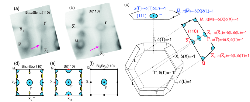
The measured Fermi surfaces for Bi(110) and Bi0.86Sb0.14(110) are shown in Fig. 1(a) and (b), respectively. They are, at first glance, very similar to each other and to published results for Bi(110) Agergaard:2001 ; Pascual:2004 . The dominating features are topologically required closed contours around the , and points as well as a small electron pocket on the line. This electron pocket does not encircle any TRIM and is irrelevant for the surface state topology, but in order to facilitate the comparison between the topological predictions and the data, it has been included as a yellow feature in Fig. 1(d),(e). The topological prediction for Bi(110) also requires the existence of a closed Fermi contour around , but this is not clearly confirmed by the data in this overview scan. In any event, such predictions do not necessarily have to be fulfilled for a semimetal because the topologically required parity changes between surface TRIMs could also be accomplished by the bulk states crossing the Fermi surface. Such projected bulk Fermi surface elements are found near the and points on Bi(110). They are indicated by the red areas in Fig. 1(e).
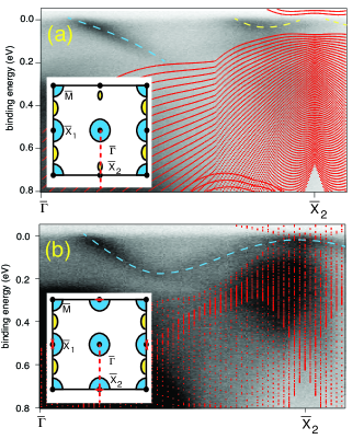
The topological quantum phase transition from Bi to Bi1-xSbx should be reflected in a change of the surface state dispersion around the point. This is consistent with the observed change between the Fermi surface maps of Fig. 1(a) and (b): While the photoemission intensity at the Fermi level near is an elongated stripe in the direction for Bi(110), this stripe is split into two features on either side of for Bi0.86Sb0.14. This situation near is further explored by a high-resolution scan along for both Bi0.86Sb0.14(110) and Bi(110) in Fig. 2. The surface state dispersion in this direction is quite different in the two cases: Both surfaces share the hole pocket around but whereas the band forming this pocket disappears into the projected band states for Bi0.86Sb0.14(110), its dispersion reaches a binding energy maximum for Bi(110) before it disperses back towards the Fermi level. It only merges with the bulk bands in the immediate vicinity of the point. For Bi0.86Sb0.14(110), on the other hand, there is no state observable at but a shallow electron pocket very close to this point.
These differences in the band structure bring the expected topology change about. For Bi(110), one would expect the point to be encircled by an odd number of Fermi contours. Experimentally, the situation is somewhat unclear because it cannot be determined if the surface state band barely crosses the Fermi level on both sides of , forming a small hole pocket around the point, or if it stays occupied. In any case, this is not important because one would not necessarily expect the topological predictions to be strictly fulfilled to for a semimetal surface. Any required change of parity could be brought about by the bulk band continuum near . For Bi0.86Sb0.14(110), on the other hand, the topological predictions should be strictly followed. In contrast to the situation for Bi(110), should not be encircled by a closed Fermi contour and it clearly is not: the shallow electron pocket marked by a yellow line is close to the point but it does not encircle it. Indeed, the electron pockets on either side of can clearly be seen in the Fermi surface scan of Fig. 1(a).
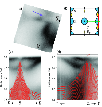
A final topological prediction for Bi0.86Sb0.14 is the existence of a closed Fermi contour around . This can already be seen in Fig. 1(a) but is shown more clearly by a detailed inspection of the band structure around this TRIM in Fig. 3. The high-resolution Fermi contour in Fig. 3(a) already shows a closed contour around in the immediate vicinity of the two electron pockets along . Scans around towards and reveal that this feature is another electron pocket. In fact, the band giving rise to it merges with the lower Rashba-split surface state bands originating from and to form a Dirac point at but this Dirac point is situated in the projected valence band. This situation and the shape of the Fermi contour around is similar to the situation on Sb(110), i.e. the case of Bianchi:2012 .
The entire Fermi contour of Bi0.86Sb0.14(110) is thus in excellent agreement with the theoretical predictions for this surface. It is also substantially more complex than that of Bi1-xSbx(111) or the predictions of the non-(111) surfaces of Bi2Se3-type topological insulators. Indeed, this illustrates the design possibilities when exploiting the surface orientation of a topological insulator. The example shown here is particularly interesting because it adds a valley degree of freedom to the topological Dirac fermions, something that is currently attracting great attention in the case of graphene Rycerz:2007 . It should also be possible to use the same strategy for the construction of quasi one-dimensional surface states on three-dimensional topological insulators, as already found for the vicinal parent surface Bi(114) Wells:2009 .
I Methods
Experiments were performed at the SGM-3 beamline of the synchrotron radiation source ASTRID Hoffmann:2004 . Thin films of Bi1-xSbx(110) were grown in situ on a Bi(110) substrate by simultaneous evaporation of Bi and Sb from an e-beam source. The Bi(110) surface had previously been cleaned by cycles of Ne ion sputtering and annealing. Data were taken for different film thicknesses and compositions. The data shown here were obtained from a film with a thickness of approximately 25 double layers and (here the term double layer is used to group the first and second layer of the A7(110) surface. These are almost at the same height Jona:1967 ; Hofmann:2006 ; Sun:2006 ). The growth rate and chemical composition of the film were determined by inspecting the shallow Sb 4d and Bi 5d core levels, as in Ref. Hirahara:2010, . The energy and angular resolution for ARPES measurements were better than 20 meV and 0.2∘, respectively. The photon energy was 28.5 eV for the data shown in Fig. 1 and 18 eV otherwise. Data were collected for many different photon energies between 14 eV and 32 eV in order to make sure that the features discussed above as surface states are in fact surface states, i.e. that their dispersion does not depend on the photon energy. The sample temperature during the measurements was 80 K. The bulk Fermi surface projections and band structure surface projection were calculated using the tight-binding parameters of Liu and Allen Liu:1995 . For the alloy, the parameters were interpolated following the method in Ref. Teo:2008, . The calculation of the surface band structure follows the transfer matrix method used in Ref. Teo:2008, but employs a Green’s function method to calculate the spectral function for a semi-infinite crystal Mele:1978 .
II Acknowledgements
We gratefully acknowledge financial support from the Carlsberg foundation, the VILLUM foundation, The Danish Council for Independent Research / Technology and Production Sciences. WSS acknowledges support by the the Brazilian funding agencies CNPq and CAPES.
References
- (1) Liang Fu and C. L. Kane. Topological insulators with inversion symmetry. Physical Review B, 76, 045302, 2007.
- (2) Liang Fu, C. L. Kane, and E. J. Mele. Topological Insulators in Three Dimensions. Physical Review Letters, 98, 106803, 2007.
- (3) J. E. Moore and L. Balents. Topological invariants of time-reversal-invariant band structures. Phys. Rev. B, 75, 121306, 2007.
- (4) Shuichi Murakami. Phase transition between the quantum spin Hall and insulator phases in 3D: emergence of a topological gapless phase. New Journal of Physics, 9, 356, 2007.
- (5) Jeffrey C. Y. Teo, Liang Fu, and C. L. Kane. Surface states and topological invariants in three-dimensional topological insulators: Application to Bi1-x Sbx. Physical Review B, 78, 045426, 2008.
- (6) Xi Dai, Taylor L. Hughes, Xiao-Liang Qi, Zhong Fang, and Shou-Cheng Zhang. Helical edge and surface states in HgTe quantum wells and bulk insulators. Phys. Rev. B, 77, 125319, 2008.
- (7) Haijun Zhang, Chao-Xing Liu, Xiao-Liang Qi, Xi Dai, Zhong Fang, and Shou-Cheng Zhang. Topological insulators in Bi2Se3, Bi2Te3 and Sb2Te3 with a single Dirac cone on the surface. Nature Physics, 5, 438–442, 06 2009.
- (8) D. Hsieh, D. Qian, L. Wray, Y. Xia, Y. S. Hor, R. J. Cava, and M. Z. Hasan. A topological Dirac insulator in a quantum spin Hall phase. Nature, 452, 970–974, 2008.
- (9) Y. Xia, D. Qian, D. Hsieh, L. Wray, A. Pal, H. Lin, A. Bansil, D. Grauer, Y. S. Hor, R. J. Cava, and M. Z. Hasan. Observation of a large-gap topological-insulator class with a single Dirac cone on the surface. Nature Physics, 5, 398–402, 2009.
- (10) Y. L. Chen, J. G. Analytis, J. H. Chu, Z. K. Liu, S. K. Mo, X. L. Qi, H. J. Zhang, D. H. Lu, X. Dai, Z. Fang, S. C. Zhang, I. R. Fisher, Z. Hussain, and Z. X. Shen. Experimental Realization of a Three-Dimensional Topological Insulator, Bi2Te3. Science, 325, 178–181, 7 2009.
- (11) K. Kuroda, H. Miyahara, M. Ye, S. V. Eremeev, Yu. M. Koroteev, E. E. Krasovskii, E. V. Chulkov, S. Hiramoto, C. Moriyoshi, Y. Kuroiwa, K. Miyamoto, T. Okuda, M. Arita, K. Shimada, H. Namatame, M. Taniguchi, Y. Ueda, and A. Kimura. Experimental Verification of as a 3D Topological Insulator. Phys. Rev. Lett., 108, 206803, May 2012.
- (12) M. Neupane, S.-Y. Xu, L. A. Wray, A. Petersen, R. Shankar, N. Alidoust, Chang Liu, A. Fedorov, H. Ji, J. M. Allred, Y. S. Hor, T.-R. Chang, H.-T. Jeng, H. Lin, A. Bansil, R. J. Cava, and M. Z. Hasan. Topological surface states and Dirac point tuning in ternary topological insulators. Phys. Rev. B, 85, 235406, Jun 2012.
- (13) Feng Lu, JianZhou Zhao, Hongming Weng, Zhong Fang, and Xi Dai. Correlated Topological Insulators with Mixed Valence. arXiv:1211.5863v1, , 2012.
- (14) Tong Zhang, Peng Cheng, Xi Chen, Jin-Feng Jia, Xucun Ma, Ke He, Lili Wang, Haijun Zhang, Xi Dai, Zhong Fang, Xincheng Xie, and Qi-Kun Xue. Experimental Demonstration of Topological Surface States Protected by Time-Reversal Symmetry. Physical Review Letters, 103, 266803, 2009.
- (15) T. Hirahara, Y. Sakamoto, Y. Saisyu, H. Miyazaki, S. Kimura, T. Okuda, I. Matsuda, S. Murakami, and S. Hasegawa. Topological metal at the surface of an ultrathin Bi1-x Sbx alloy film. Phys. Rev. B, 81, 165422, Apr 2010.
- (16) C. Brüne, C. X. Liu, E. G. Novik, E. M. Hankiewicz, H. Buhmann, Y. L. Chen, X. L. Qi, Z. X. Shen, S. C. Zhang, and L. W. Molenkamp. Quantum Hall Effect from the Topological Surface States of Strained Bulk HgTe. Phys. Rev. Lett., 106, 126803, 2011.
- (17) H. Berger, B. Christ, and J. Troschke. Lattice Parameter Study in the Bi1–xSbx Solid-solution System. Crystal Research and Technology, 17, 1233–1239, 1982.
- (18) S. Agergaard, C. Søndergaard, H. Li, M. B. Nielsen, S. V. Hoffmann, Z. Li, and Ph. Hofmann. The effect of reduced dimensionality on a semimetal: The electronic structure of the Bi(110) surface. New Journal of Physics, 3, 15.1–15.10, 2001.
- (19) J. I. Pascual, G. Bihlmayer, Y. M. Koroteev, H. P. Rust, G. Ceballos, M. Hansmann, K. Horn, E. V. Chulkov, S. Blugel, P. M. Echenique, and Ph. Hofmann. Role of spin in quasiparticle interference. Physical Review Letters, 93, 196802, 2004.
- (20) Marco Bianchi, Dandan Guan, Anna Stróżecka, Celia H. Voetmann, Shining Bao, Jose Ignacio Pascual, Asier Eiguren, and Philip Hofmann. Surface states on a topologically nontrivial semimetal: The case of Sb(110). Phys. Rev. B, 85, 155431, Apr 2012.
- (21) A. Rycerz, J. Tworzydlo, and C. W. J. Beenakker. Valley filter and valley valve in graphene. Nature Physics, 3, 172–175, 03 2007.
- (22) J. W. Wells, J. H. Dil, F. Meier, J. Lobo-Checa, V. N. Petrov, J. Osterwalder, M. M. Ugeda, I. Fernandez-Torrente, J. I. Pascual, E. D. L. Rienks, M. F. Jensen, and Ph. Hofmann. Nondegenerate Metallic States on Bi(114): A One-Dimensional Topological Metal. Physical Review Letters, 102, 096802, 2009.
- (23) S. V. Hoffmann, C. Søndergaard, C. Schultz, Z. Li, and Ph. Hofmann. An undulator-based spherical grating monochromator beamline for angle-resolved photoemission spectroscopy. Nuclear Instruments and Methods in Physics Research, A, 523, 441, 2004.
- (24) F. Jona. Low-energy electron diffraction study of surfaces of antimony and bismuth. Surface Science, 8, 57–76, 1967.
- (25) Ph. Hofmann. The surfaces of bismuth: Structural and electronic properties. Progress in Surface Science, 81, 191–245, 2006.
- (26) J. Sun, A. Mikkelsen, M. Fuglsang Jensen, Y. M. Koroteev, G. Bihlmayer, E. V. Chulkov, D. L. Adams, Ph. Hofmann, and K. Pohl. Structural determination of the Bi(110) semimetal surface by leed analysis and ab initio calculations. Physical Review B, 74, 245406, 2006.
- (27) Yi Liu and Roland E. Allen. Electronic structure of the semimetals Bi and Sb. Physical Review B, 52, 1566, 1995.
- (28) Eugene J. Mele and J. D. Joannopoulos. Electronic states at unrelaxed and relaxed GaAs (110) surfaces. Phys. Rev. B, 17, 1816–1827, Feb 1978.