GW quasiparticle band structures of stibnite, antimonselite,
bismuthinite, and guanajuatite
Abstract
We present first-principles calculations of the quasiparticle band structures of four isostructural semiconducting metal chalcogenides A2B3 (with A = Sb, Bi and B = S, Se) of the stibnite family within the G0W0 approach. We perform extensive convergence tests and identify a sensitivity of the quasiparticle corrections to the structural parameters and to the semicore electrons. Our calculations indicate that all four chalcogenides exhibit direct band gaps, if we exclude some indirect transitions marginally below the direct gap. Relativistic spin-orbit effects are evaluated for the Kohn-Sham band structures, and included as scissor corrections in the quasiparticle band gaps. Our calculated band gaps are 1.5 eV (Sb2S3), 1.3 eV (Sb2Se3), 1.4 eV (Bi2S3) and 0.9 eV (Bi2Se3). By comparing our calculated gaps with the ideal Shockley-Queisser value we find that all four chalcogenides are promising as light sensitizers for nanostructured photovoltaics.
pacs:
71.20.-b 74.70.Xa 78.20.-e 78.56.-aI Introduction
The development of sustainable energy solutions based on scalable processes and non-toxic materials constitutes a key priority in the current scientific research agenda, and in this area nanostructured energy-harvesting solar and thermoelectric devices are playing a lead role. Recently there has been a surge of interest in devices using semiconducting metal chalcogenides of the stibnite family. For example recent studies have demonstrated the potential of these semiconductors both in photovoltaics applications,Chang et al. (2010, 2012); Rath et al. (2012); Guijarro et al. (2012) and in thermoelectric generators.Mehta et al. (2010)
In the area of nanostructured photovoltaics semiconducting metal chalcogenides have successfully been used to replace the inorganic dye in dye-sensitized solar cells,O’Regan and Grätzel (1991) leading to the development of solid-state semiconductor-sensitized solar cells.Hodes (2008); Chang et al. (2010) In these devices thin layers or nanoparticles of the semiconducting chalcogenides act as light absorbers, and upon photoexcitation they transfer an electron to the acceptor (typically TiO2) and a hole to the hole-transporter (for example a conducting polymer). The record efficiency within this class of devices is 5.1% and was obtained using stibnite (Sb2S3) as semiconductor sensitizer.Chang et al. (2010)
A recent atomistic computational study of photovoltaic interfaces for semicondictor-sensitized solar cells pointed out that, in addition to stibnite, the other members of the stibnite mineral family, namely antimonselite (Sb2Se3), bismuthinite (Bi2S3), and guanajuatite (Bi2Se3), exhibit optical properties similar to stibnite and should be considered as potential candidates for novel semiconductor sensitizers.Patrick and Giustino (2011) Using density-functional calculations and empirical scissor corrections of the band gaps, in Ref. Patrick and Giustino, 2011 it was found that stibnite and antimonselite should form type-II heterojunctions with TiO2, while bismuthinite should form a type-I heterojunction and hence would not be able to transfer electrons to TiO2. These theoretical predictions have recently been confirmed by the experimental investigations of Refs. Guijarro et al., 2012; Lutz et al., 2012, thereby providing a motivation for further studies and for the more sophisticated analysis presented in this work.
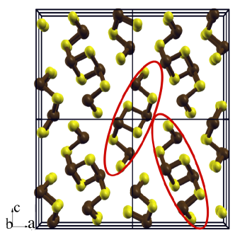
The four minerals of the stibnite family crystallize in an orthorhombic structure consisting of parallel one-dimensional (A4B6)n ribbons, with A = Sb, Bi and B = S, Se. A ball-and-stick model of this structure is shown in Fig. 1. Besides its natural occurrence in mineral form, stibnite can be synthesised using a variety of low-cost fabrication techniques.Bhosale et al. (1994); Versavel and Haber (2007); Lokhande et al. (2002); Maghraoui-Meherzi et al. (2010); Cademartiri et al. (2008); Malakooti et al. (2008); Rühle et al. (2010); Han et al. (2011); Cademartiri et al. (2012) Using these techniques it is possible to obtain a good degree of crystallinity,Rincon et al. (1998); Perales et al. (2007) to control dimensionality,Rühle et al. (2010); Bao et al. (2007); Mehta et al. (2010) and to tune the optical properties.Vedeshwar (1995); Karguppikar and Vedeshwar (1987); Rühle et al. (2010); Deng et al. (2009)
Semiconductors of the stibnite family have also been synthesized in various nanostructured forms. For example Refs. Cademartiri et al., 2008; Malakooti et al., 2008; Mehta et al., 2010 and Refs. Mehta et al., 2010; Deng et al., 2009 reported nanowires and nanotubes, respectively, of stibnite, antimonselite and bismuthinite. Nanowires of stibnite were found to exhibit enhanced ferroelectric and piezoelectric properties as compared to their bulk counterpart.Varghese et al. (2012) Nanowires and nanotubes of antimonselite were found to exhibit conductivities much higher than their bulk counterpart,Mehta et al. (2010) and are being considered for thermoelectric applications. In the case of bismuthinite, Ref. Cademartiri et al., 2008 reported nanowires with diameters as small as 1.6 nm, corresponding to a transverse size of only two ribbons. The rhombohedral phase of Bi2Se3 has been investigated extensively since this compound is a prototypical topological insulator.Zhang et al. (2009) However to the best of our knowledge little is known about orthorhombic Bi2Se3, i.e. guanajuatite, which is stable only at high temperature and pressure.Atabaeva et al. (1973); Okamoto (1994)
The band gaps of stibnite, antimonselite and bismuthinite have been measured extensively via optical absorption experiments. The band gap of stibnite ranges between 1.42-1.78 eV.Mahanty et al. (1997); El Zawawi et al. (1998) For antimonselite Ref. Torane et al., 1999 reported a direct gap of 1.55 eV, while Ref. Rodriguez-Lazcano et al., 2005 gave an indirect gap between 1-1.2 eV. The measured band gap of bismuthinite is 1.38-1.58 eV.Lukose and Pradeep (1991); Mahmoud et al. (1997); Yesugade et al. (1995) The spread in the measured gaps can be attributed to the different preparation conditions used, yielding different degrees of polycrystallinity and even amorphous samples in some cases, and also different stoichiometries. In addition all these compounds exhibit closely lying direct and indirect transitions (cf. Fig. 3 below), thereby complicating the assignment of the nature of the optical gap.
All four minerals of the stibnite family have been investigated in detail using density-functional theory (DFT) calculations. The electronic properties of these compounds have been studied in Refs. Caracas and Gonze, 2005; Vadapoo et al., 2011a; Larson et al., 2002; Koc et al., 2012; Sharma and Srivastava, 2010; Sharma et al., 2012; Ben Nasr et al., 2011; Patrick and Giustino, 2011, and the elastic and optical properties have been calculated in Ref. Koc et al., 2012.
A comparison of the theoretical studies published so far shows some inconsistencies in the calculated band gaps, for example the values reported for stibnite are in the range 1.18-1.55 eV.Caracas and Gonze (2005); Patrick and Giustino (2011); Vadapoo et al. (2011b); Koc et al. (2012) As expected all the calculated DFT gaps underestimate the measured band gaps. To the best of our knowledge only one workVadapoo et al. (2011b) reported a calculation of the quasiparticle band gap of stibnite and antimonselite within the GW approximation.Hedin (1965) The electronic structure of the rhombohedral Bi2Se3 has also been explored within the GW approach Yazyev et al. (2012).
Within this context there exists a need for detailed and reproducible calculations of the electronic structure of stibnite and related compounds based on state-of-the-art quasiparticle techniques. In line with this need the goal of the present work is to report a systematic and reproducible study of the quasiparticle band structures of all four A2B3 semiconducting metal chalcogenides of the stibnite family. An emphasis is placed on convergence tests and on the sensitivity of the quasiparticle corrections to the structural parameters, the inclusion of semicore states in the calculations, and relativistic effects.
Our calculated band gaps are 1.5 eV (Sb2S3), 1.3 eV (Sb2Se3), 1.4 eV (Bi2S3) and 0.9 eV (Bi2Se3). By inspection of the band structures we infer that all four compounds have direct band gaps, although in most cases an indirect transition just below the direct gap (within 0.1 eV) is also possible. The inclusion of semicore electrons in the calculations is found to modify the band gaps by 0.1-0.2 eV. In addition we find that the gaps are rather sensitive to the lattice parameters, as they change by up to 0.3 eV when the lattice parameters are taken from experiment or fully optimized within DFT. Relativistic corrections are found to be essentially negligible for Sb2S3 and Sb2Se3, while in the case of Bi2S3 and Bi2Se3 the band gaps decrease by 0.3-0.4 eV upon inclusion of spin-orbit coupling.
The manuscript is organized as follows. In Sec. II we describe the computational methodology and the convergence tests for the GW calculations. In Sec. III we present our main results, including quasiparticle band structures and band gaps. In Sec. IV we discuss our findings in relation to the photovoltaics applications of the materials considered in this work. In Sec. V we summarize our results and present our conclusions.
II Methodology
II.1 DFT calculations
All DFT calculations are performed using the Quantum ESPRESSO package.Giannozzi et al. (2009) The calculations are based on the local density approximation (LDA) to DFT.Perdew and Zunger (1981); Ceperley and Alder (1980)
Only valence electrons are explicitly described, and the core-valence interaction is taken into account by means of Troullier-Martins scalar relativistic pseudopotentialsTroullier and Martins (1991) generated using the fhi98 code.Fuchs and Scheffler (1999) In the cases of S (Se) the () electrons are included in the valence as usual. For Sb and Bi we generate two sets of pseudopotentials, one set with five electrons in the valence, i.e. and respectively, and one set with additional semicore and electrons, respectively.
The electronic wavefunctions are expanded in planewaves basis sets with kinetic energy cutoffs of 70 Ry (Sb2Se3, Bi2Se3) and 90 Ry (Sb2S3, Bi2S3) for the calculations without semicore states, and 100 Ry (Bi2S3, Bi2Se3) and 130 Ry (Sb2S3, Sb2Se3) when semicore states are included. In each case considered the selected cutoff yields a total energy converged to within 2 meV/atom. All self-consistent calculations are carried out using a 888 Brillouin zone mesh centered at , corresponding to 170 irreducible points for Sb2S3 and Bi2S3, and 260 points for Sb2Se3 and Bi2Se3.
We perform full geometry optimizations of the lattice parameters and the atomic positions in each case, both with or without semicore states. All structural optimizations are performed using 484 -centered Brillouin zone meshes.
II.2 Crystal structure
Stibnite (Sb2S3), antimonselite (Sb2Se3), bismuthinite (Bi2S3), and guanajuatite (Bi2Se3) all crystallize in the same orthorhombic lattice and belong to the Pnma 62 space group.Caracas and Gonze (2005) Each unit cell contains 20 atoms, whose coordinates can be generated by applying the symmetry operations of the crystallographic group to a set of 5 atomic coordinates. Figure 1 shows a ball-and-stick representation of these A2B3 structures. The structural parameters were measured by Refs. Bayliss and Nowacki, 1972; Voutsas et al., 1985; Kanishcheva et al., 1981; Atabaeva et al., 1973 and are reported in Ref. Caracas and Gonze, 2005.
As the crystal structure consists of a bundle of relatively well separated ribbons, it is convenient to separate the cohesive energy into intra-ribbon and inter-ribbon components. The intra-ribbon cohesive energy is calculated as the difference between the total energy of one ribbon and the total energies of its consituent atoms. The inter-ribbon cohesive energy is evaluated as the difference between the total energy of the unit cell and twice the total energy of one ribbon in isolation (each unit cell contains two ribbons).
II.3 Quasiparticle calculations
We calculate the quasiparticle energies within many-body perturbation theory using the GW method,Hedin (1965); Hybertsen and Louie (1986b); Aulbur et al. (1999); Aryasetiawan and Gunnarsson (1998); Onida et al. (2002) as implemented in the SaX code.Martin-Samos and Bussi (2009) The GW self-energy is evaluated in the G0W0 approximation as . Here denotes the electron Green’s function defined by the Kohn-Sham eigenstates and eigenvalues corresponding to the band index and the wavevector , and represents the screened Coulomb interaction calculated in the random phase approximation.Hedin and Lundqvist (1969); Hybertsen and Louie (1986b) The quasiparticle energies are obtained as:Hybertsen and Louie (1986b)
| (1) |
where is the quasiparticle energy, the associated quasiparticle renormalization, and is the exchange and correlation potential.
The self-energy can be written as the sum of a bare exchange contribution and a correlation contribution : . The exchange part does not depend explicitly on the excitation energy and reads:Giustino et al. (2010)
| (2) |
where the sum is over occupied states and represents the bare Coulomb interaction. This contribution to the quasiparticle correction is sensitive to the overlap between Kohn-Sham wavefunctions regardless of their energy. As a result the use of semicore states can have significant effect on the calculations, as shown in Refs. Rohlfing et al., 1995; Tiago et al., 2004; Umari and Fabris, 2012. This aspect will be discussed in detail in Sec. III.3.
The energy-dependence of the correlation contribution arising from the dynamically-screened Coulomb interaction is described via the Godby-Needs plasmon-pole model.Godby and Needs (1989) We use a plasmon-pole energy of 1 Ry for all materials, similar to the energy of the peaks in the calculated electron energy loss spectra.
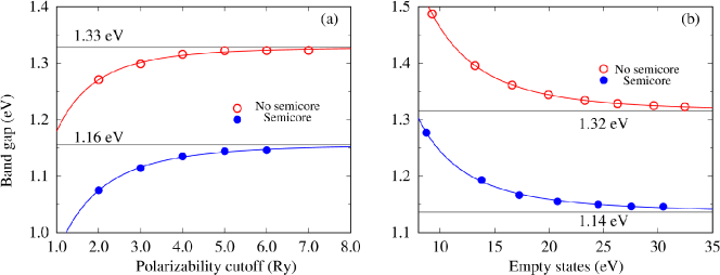
Since the computational efforts for achieving convergence in and are very different owing to the necessity of evaluating unoccupied states for , we perform separate convergence tests for these two components. For the exchange contribution we use kinetic energy cutoffs of 75 Ry and 100 Ry for calculations without and with semicore electrons, respectively. For the correlation contribution we perform convergence tests by calculating the band gap at various kinetic energy cutoffs up to 7 Ry for the polarizability. Figure 2(a) shows that the band gap is converged within 0.05 eV already for a cutoff of 5 Ry. The dependence of the band gap on the polarizability cutoff shows the same trend for calculations with or without semicore states. This is consistent with the expectation that the effect of semicore states in should be small.Rohlfing et al. (1995) Based on the data of Fig. 2(a), in the following we use a polarizability cutoff of 7 Ry for calculations without semicore electrons, and of 6 Ry for the more demanding calculations including semicore states. In Fig. 2(b) we show the convergence of the band gap of antimonselite with respect to the energy of the highest unoccupied state included in the polarizability. Based on the trend in this figure we set the number of unoccupied states to 224 and 264 for calculations with and without semicore, corresponding to a maximum energy denominator of 35 eV. Both and are calculated on uniform and -centered 262 Brillouin-zone meshes.
In order to estimate the accuracy of our quasiparticle corrections with respect to the above convergence parameters we follow the approach of Ref. 65. In this approach the dependence of the band gap on a given convergence parameter is fitted by a simple function in order to extract a “best-guess” asymptotic limit. This asymptotic limit is then taken to represent the converged gap. In this work we tentatively approximate gap vs. cutoff curves using the following function:
| (3) |
where is the quasiparticle band gap, is the convergence parameter (i.e. the polarizability cutoff or the largest energy denominator) and are fitting parameters. While Eq. (3) is largely arbitrary, this choice reflects the expectation that the gap will converge faster than owing to the damping introduced by the matrix elements in the Adler-Wiser polarizability.Adler (1962); Wiser (1963) Figure 2 shows that the fitting curves obtained for stibnite describe rather accurately the calculated data points, therefore it is reasonable to assume that the parameter obtained from the fit should provide a good estimate of the converged gap. By repeating this procedure for all four compounds Sb2S3, Sb2Se3, Bi2S3, and Bi2Se3 we find that the convergence parameters described above yield band gaps which differ by less than 0.05 eV from the corresponding asymptotic values.
II.4 Spin-orbit coupling
Owing to the high atomic numbers of Bi and Sb, it is important to check the role of spin-orbit coupling (SOC) in the electronic structure of semiconductors of the stibnite family. In this work we evaluate SOC effects at the DFT level, by constructing a set of fully-relativistic Troullier-Martins pseudopotentials including semicore states. The pseudopotentials are generated using the ld1.x program of the Quantum ESPRESSO package. We checked that the planewaves cutoffs described in Sec. II.1 for scalar-relativistic calculations are also appropriate for these fully-relativistic pseudopotentials. For S and Se relativistic effects are not expected to be significant, and scalar-relativistic pseudopotentials are used throughout. We determine the spin-orbit corrections to the band gaps by taking the differences between self-consistent calculations using the fully-relativistic pseudopotentials with or without noncollinear magnetism.Oda et al. (1998) We then apply these differences as scissor corrections to the corresponding quasiparticle band gaps obtained from scalar relativistic calculations.
III Results
III.1 Structural parameters
Table 1 shows the comparison between our calculated lattice parameters and experiment. As expected the use of the local density approximation leads to a general underestimation of the experimental parameters. Interestingly, while such underestimation does not exceed 1.1% along the direction of the (A4B6)n ribbons ( parameter in Table 1, cf. Fig. 1), the deviation can reach up to 4.2% in the direction perpendicular to the ribbons ( and parameters in Table 1). We tentatively assign this behavior to the fact that inter-ribbon forces are likely to include non-negligible van der Waals components, and hence are not described correctly within the LDA.
Inspection of the calculated cohesive energies seems to support this possibility. Indeed we obtain intra-ribbon cohesive energies of 3.9 eV/atom (Sb2S3), 3.5 eV/atom (Sb2Se3) 3.6 eV/atom (Bi2S3) and 3.3 eV/atom (Bi2Se3). The inter-ribbon cohesive energy are one order of magnitude smaller, 0.2 eV/atom (Sb2S3 and Sb2Se3) and 0.3 eV/atom (Bi2S3 and Bi2Se3).
We also performed additional calculations of the structural parameters using the van der Waals functional of Ref. Dion et al., 2005. The lattice parameters calculated using the vdW functional overestimate the experimental values by up to 6.9% along the directions perpendicular to the ribbons, while along the ribbons the calculated parameters are in agreement with experiment (within 0.3%). Similar trends have been observed in calculations on graphite and boron nitride in Ref. Langreth et al., 2005. These results indicate that for semiconductors of the stibnite family the use of a van der Waals functional does not improve the agreement of the calculated structural parameters with experiment.
In order to take into account the differences between calculated and experimental lattice parameters, in the following we report quasiparticle calculations obtained using either the DFT/LDA structure or the experimental structure.
| Experiment | Calc. w/o semicore | Calc. with semicore | |||||||||
| Sb2S3 | 11.311a | 3.836a | 11.229a | 11.036 | 3.795 | 10.753 | 11.087 | 3.838 | 10.834 | ||
| -2.4% | -1.1% | -4.2% | -2.0% | 0.1% | -3.5% | ||||||
| Sb2Se3 | 11.794b | 3.986b | 11.648b | 11.609 | 3.952 | 11.213 | 11.646 | 3.989 | 11.287 | ||
| -1.6% | -0.9% | -3.7% | -1.3% | 0.1% | -3.1% | ||||||
| Bi2S3 | 11.305c | 3.981c | 11.147c | 11.227 | 3.999 | 11.001 | 11.030 | 3.949 | 10.853 | ||
| -0.7% | 0.5% | -1.3% | -2.4% | -0.8% | -2.6% | ||||||
| Bi2Se3 | 11.830d | 4.090d | 11.620d | 11.767 | 4.141 | 11.491 | 11.609 | 4.099 | 11.374 | ||
| -0.5% | 1.3% | -1.1% | -1.9% | 0.2% | -2.1% | ||||||
| a Ref. 51. | |||||||||||
| b Ref. 52. | |||||||||||
| c Ref. 53. | |||||||||||
| d Ref. 27. | |||||||||||
| Mimimum gap | Direct gap | ||||
|---|---|---|---|---|---|
| w semicore | w/o semicore | w semicore | w/o semicore | ||
| Sb2S3 | 1.19 | 1.21 | 1.26 | 1.27 | |
| Sb2Se3 | 0.84 | 0.86 | 0.84 | 0.86 | |
| Bi2S3 | 1.25 | 1.24 | 1.28 | 1.27 | |
| Bi2Se3 | 0.85 | 0.86 | 0.99 | 0.99 | |
III.2 DFT/LDA band structures
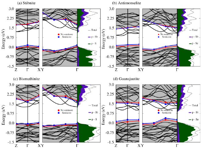
Figure 3 shows the DFT/LDA band structures calculated using experimental lattice parameters and without semicore electrons. Calculations including the semicore states yield very similar band structures. For clarity we only show the dispersions along the -- path and along the - segment running along the axis of the (A4B6)n ribbons. The top of the valence band is found to be predominantly of S-3 or Se-4 character, while the bottom of the conduction band comprises of Sb-5 or Bi-6 states, consistently with previous calculations.Caracas and Gonze (2005); Ben Nasr et al. (2011)
The band structures shown in Fig. 3 exhibit several extrema in proximity of the fundamental gap, making the direct and indirect transitions almost degenerate. Table 2 shows that the energy separation between direct and indirect DFT/LDA band gaps falls within 0.15 eV in all cases. The data in the table suggest that in these compounds the direct transition will most likely dominate over the indirect one, apart from a very narrow onset of 0.1-0.2 eV. This observation is consistent with experimental evidence showing a weak absorption onset just below the threshold for direct absorption.El Zawawi et al. (1998); Versavel and Haber (2007) Therefore for practical purposes, and in particular for photovoltaics applications, stibnite, antimonselite, bismuthinite and guanajuatite can be considered as “effectively direct gap” semiconductors.
III.3 Quasiparticle corrections
Figure 3 shows that GW quasiparticle corrections lead to a moderate increase of the band gaps in all cases, while generally preserving the shape of the band extrema. From this figure we deduce that a simple scissor operator should be able to capture the most important effects of the GW corrections.
A detailed analysis of the quasiparticle corrections at the high-symmetry points , , and is given in Fig. 4 and Table 3. In Fig. 4 we report the quasiparticle corrections as a function of the corresponding Kohn-Sham eigenvalues around the band extrema. In the cases of stibnite and antimonselite we observe that in the calculations with semicore electrons the valence bands are slightly upshifted (by about 0.1 eV) as compared to calculations without semicore, while the corrections to the conduction bands are essentially the same. In the cases of bismuthinite and guanajuatite the effect of semicore is to shift the valence bands up and the conduction bands down by a similar amount (0.1 eV). As a result of these small changes, the quasiparticle corrections to the band gaps calculated with or without semicore electrons can differ by up to 0.2 eV (cf. Table 3).
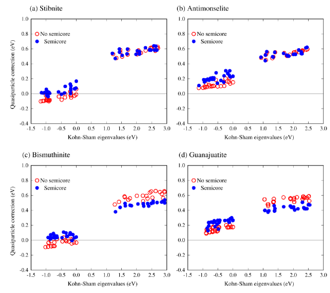
Semicore electrons appear to slightly reduce the quasiparticle corrections as compared to calculations without the semicore. This finding is consistent with previous calculations and can be rationalized as follows.Rohlfing et al. (1995); Tiago et al. (2004); Umari and Fabris (2012) The semicore states introduce additional contributions and to the GW self energy. Of these contributions, while the correlation part is small owing to the large energy separation between semicore states and conduction states, the exchange part can be large since it does not contain energy denominators but is sensitive to the overlap between the band edge states and the semicore states. This interpretation is confirmed by Fig. 5, where we can see that the inclusion of semicore electrons does indeed affect the exchange part of the GW corrections, while at the same time the correlation component remains almost unchanged.
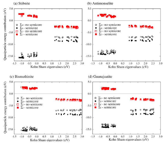
Table 3 reports the DFT/LDA eigenvalues and the corresponding quasiparticle corrections for the valence band top and conduction band bottom at the high symmetry points , and . From this table we see that the LDA band gaps at these points are sensitive to the choice of the lattice parameters, and this sensitivity is reflected in the corresponding quasiparticle energies. Calculations performed using optimized lattice parameters or experimental parameters can differ by up to 0.3 eV. This observation may explain the lack of consensus between previous computational investigations of the band structures of these compounds.Caracas and Gonze (2005); Patrick and Giustino (2011); Vadapoo et al. (2011b); Koc et al. (2012)
Taken together the sensitivity of the quasiparticle energies to the presence of semicore electrons and to the choice of lattice parameters leads to non-negligible variations in the calculated band gaps. This suggests that it is important to use some care when comparing the quasiparticle band structures of stibnite and related compounds with experimental data.
In the remainder of this manuscript we will focus on calculations using experimental lattice parameters and including semicore electrons, which we consider our best estimates for the quasiparticle energies in these compounds.
III.4 Relativistic corrections
We calculate the relativistic corrections within DFT/LDA for all four structures using the experimental structure. The corrections to the band edges at the high-symmetry points , and are reported in Table 4.
In all four semiconductors the inclusion of spin-orbit coupling does not alter the top of the valence band. This is consistent with the observation that the states at the valence band top are predominantly associated with S or Se states. On the other hand the bottom of the conduction bands are of Bi or Sb character (see Fig. 3), hence a spin-orbit splitting is expected in this case. We calculate indeed a very small spin-orbit splitting for Sb2S3 and Sb2Se3, which has the effect of lowering the conduction band minima by less than 0.1 eV. In the case of Bi2S3 and Bi2Se3 the spin-orbit splitting is as large as 0.3-0.4 eV, consistent with the higher atomic number of Bi.
III.5 Band gaps
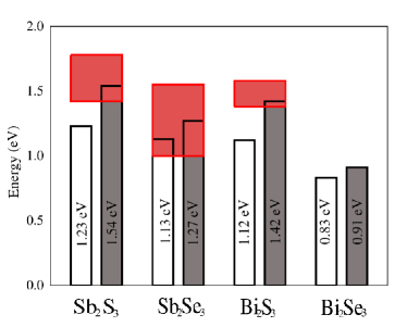
Table 5 reports the quasiparticle band gaps calculated using the experimental structures, including semicore electrons and relativistic corrections. The band gaps are obtained by considering the band extrema at , and Z and we give both the fundamental gap and the direct gap. While in antimonselite, and bismuthinite the calculated minimum gap is indirect, the difference between direct and indirect gaps is within 0.1 eV. In guanajuatite and stibnite the fundamental gap is direct. These results suggest that all four compounds can be considered direct-gap semiconductors for practical applications, especially in the area of optoelectronics. The calculated direct gaps are 1.54 eV (stibnite), 1.27 eV (antimonselite), 1.42 eV (bismuthinite), and 0.91 eV (guanajuatite). As shown in Table 5 these values are in line with previous GW calculations where available,Vadapoo et al. (2011a, b) and also rather close to measured optical gaps.
The comparison with experimental data is not straightforward since the experimental literature appears to only report optical gaps (cf. literature review in Table 5). However our calculations refer to quasiparticle gaps and do not include excitonic effects. Including excitonic effects using the Bethe-Salpeter approachOnida et al. (2002) would be rather challenging owing to the large size of these systems. To the best of our knowledge no excitonic effects were measured or mentioned for any of the four compounds studied. One exception is possibly the absorption spectrum reported in Ref. Versavel and Haber, 2007, which exhibits some sharp features resembling excitonic peaks, however the authors assigned those peaks to defects or internal reflections. The agreement between our calculated quasiparticle gaps and the measured optical gaps can be seen a posteriori as an indication that excitonic shifts are small in this class of semiconductors.
Figure 6 provides a schematic view of our final calculated band gaps (GW + SOC) compared to the Kohn Sham band gaps (DFT/LDA + SOC) and experiment.
| Optimized parameters | Expt. parameters | |||||||
| LDA | GW | LDA | GW | |||||
| w/o S | S | w/o S | S | w/o S | S | w/o S | S | |
| Stibnite | ||||||||
| 0.00 | 0.00 | 0.10 | 0.20 | 0.00 | 0.00 | 0.06 | 0.17 | |
| 1.15 | 1.11 | 1.58 | 1.52 | 1.33 | 1.29 | 1.81 | 1.77 | |
| -0.05 | -0.03 | -0.03 | 0.09 | 0.00 | -0.01 | -0.02 | 0.06 | |
| 1.40 | 1.39 | 1.90 | 1.88 | 1.46 | 1.43 | 2.01 | 1.99 | |
| -0.16 | -0.14 | -0.14 | -0.04 | -0.06 | -0.06 | -0.08 | 0.01 | |
| 1.17 | 1.17 | 1.65 | 1.65 | 1.22 | 1.20 | 1.75 | 1.74 | |
| Antimonselite | ||||||||
| -0.12 | -0.12 | 0.07 | 0.18 | -0.11 | -0.11 | 0.11 | 0.20 | |
| 0.97 | 0.91 | 1.40 | 1.32 | 1.09 | 1.07 | 1.54 | 1.52 | |
| 0.00 | 0.00 | 0.19 | 0.29 | 0.00 | 0.00 | 0.15 | 0.23 | |
| 1.05 | 1.00 | 1.53 | 1.46 | 1.10 | 1.08 | 1.62 | 1.60 | |
| -0.23 | -0.24 | -0.06 | 0.02 | -0.09 | -0.09 | 0.04 | 0.14 | |
| 0.92 | 0.91 | 1.37 | 1.35 | 0.94 | 0.93 | 1.42 | 1.42 | |
| Bismuthinite | ||||||||
| -0.10 | -0.04 | -0.04 | 0.08 | -0.14 | -0.12 | -0.14 | -0.04 | |
| 1.14 | 1.14 | 1.57 | 1.48 | 1.28 | 1.30 | 1.76 | 1.68 | |
| 0.00 | 0.00 | 0.02 | 0.09 | 0.00 | 0.00 | -0.03 | 0.04 | |
| 1.50 | 1.67 | 2.04 | 2.09 | 1.61 | 1.63 | 2.18 | 2.09 | |
| -0.15 | -0.11 | -0.13 | -0.04 | -0.08 | -0.07 | -0.11 | -0.04 | |
| 1.43 | 1.51 | 1.89 | 1.93 | 1.41 | 1.45 | 1.93 | 1.89 | |
| Guanajuatite | ||||||||
| -0.02 | -0.02 | 0.18 | 0.30 | -0.07 | -0.04 | 0.11 | 0.26 | |
| 0.95 | 0.89 | 1.39 | 1.24 | 1.17 | 1.16 | 1.63 | 1.54 | |
| 0.00 | 0.00 | 0.19 | 0.28 | 0.00 | 0.00 | 0.18 | 0.27 | |
| 1.07 | 1.18 | 1.61 | 1.58 | 1.04 | 1.06 | 1.59 | 1.45 | |
| -0.24 | -0.19 | -0.06 | 0.05 | -0.14 | -0.12 | 0.04 | 0.12 | |
| 1.17 | 1.25 | 1.63 | 1.65 | 1.16 | 1.18 | 1.64 | 1.57 | |
| Sb2S3 | Sb2Se3 | Bi2S3 | Bi2Se3 | |||||||||||||
|---|---|---|---|---|---|---|---|---|---|---|---|---|---|---|---|---|
| w/o SOC | SOC | w/o SOC | SOC | w/o SOC | SOC | w/o SOC | SOC | |||||||||
| 0.00 | 0.00 | -0.11 | 0.00 | -0.12 | -0.02 | -0.04 | -0.01 | |||||||||
| 1.29 | -0.06 | 1.07 | -0.05 | 1.30 | -0.32 | 1.16 | -0.38 | |||||||||
| -0.01 | 0.00 | 0.00 | 0.00 | 0.00 | -0.02 | 0.00 | -0.02 | |||||||||
| 1.43 | -0.04 | 1.08 | -0.03 | 1.63 | -0.40 | 1.06 | -0.27 | |||||||||
| -0.06 | 0.00 | -0.09 | 0.00 | -0.07 | -0.02 | -0.12 | -0.01 | |||||||||
| 1.20 | -0.02 | 0.93 | -0.02 | 1.45 | -0.31 | 1.18 | -0.28 | |||||||||
| Previous | Present | Previous | Present | Experiment | |||||
|---|---|---|---|---|---|---|---|---|---|
| DFT | DFT+SOC | GW | GW+SOC | ||||||
| Sb2S3 | 1.55a, 1.76b, 1.3c, 1.18d, 1.22e | 1.23 | 1.67e | 1.54 | 1.73f, 1.42-1.65g, 1.78h, 1.7i, 1.74j | ||||
| Sb2Se3 | 1.14a, 0.99d, 0.79k, 0.89e | 1.13 (0.91) | 1.21k | 1.27 (1.17) | 1.55l, 1.2i, 1.0 - 1.2m | ||||
| Bi2S3 | 1.47a, 1.32n, 1.63n, 1.45n, 1.67n | 1.12 (1.00) | 1.42 (1.34) | 1.4o, 1.38p, 1.58q,j | |||||
| Bi2Se3 | 0.9a, 1.1r | 0.83 | 0.91 | ||||||
| a Ref. 36, b Ref. 42, c Ref. 8, d Ref. 39, e Ref. 43, f Ref. 11, | |||||||||
| g Ref. 29, h Ref. 30, i Ref. 71, j Ref. 35,k Ref. 37, l Ref. 31, m Ref. 32, | |||||||||
| n Ref. 41, o Ref. 72, p Ref. 33, q Ref. 34, r Ref. 40 | |||||||||
IV Discussion
Taking the calculated quasiparticle band gaps of 0.9-1.5 eV as representative of the optical gaps, the four semiconductors considered here lie precisely in the range of the optimal Shockley-Queisser performance.Shockley and Queisser (1961) The Shockley-Queisser analysis addresses the ultimate efficiency of a solar cell based on a single material as light absorber and electron conductor, e.g. silicon solar cells. In this analysis the optimum efficiency results from a trade-off between maximizing the band gap in order to increase the photovoltage, and minimizing the band gap in order to increase the photocurrent.Shockley and Queisser (1961)
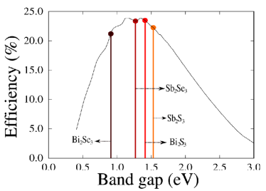
In the case of nanostructured solar cells based on the donor/acceptor concept such as for instance semiconductor-sensitized solar cells,Hodes (2008); Chang et al. (2010) the Shockley-Queisser analysis needs to be modified in order to take into account the energy-level alignment at the donor/acceptor interface. In fact, while the photocurrent is still determined by the optical gap of the absorber (typically the donor), at variance with conventional bulk solar cells the photovoltage is dictated by the difference between the lowest unoccupied states of the acceptor and the highest occupied states of the donor. This effect can be taken into account by introducing the concept of “loss-in-potential”,Snaith (2010) which is the reduction of the photovoltage resulting from the energy mismatch and additional losses. Loss-in-potentials estimated for actual devices can be as large as eV, and the most optimistic scenario would correspond to losses as small as 0.3 eV.Snaith (2010) Figure 7 shows the theoretical efficiency of semiconductor-sensitized solar cells based on stibnite, antimonselite, bismuthinite, and guanajuatite, calculated using the prescription of Ref. Snaith, 2010 for a loss-in-potential of 0.3 eV. While these estimates are very crude and the projections are possibly too optimistic, it is interesting to note that all of these four materials cluster very near the optimum power conversion efficiency of 20-25%.
From Fig. 7 we infer that the four compounds studied here are all promising candidate for nanostructured photovoltaic applications, with antimonselite and bismuthinite slightly superior to stibnite. In particular it cannot be excluded that guanajuatite, even if unstable at room temperature in bulk form, could be stabilized as a nanostructure. Given its projected maximum efficiency in Fig. 7, it might be worth to attempt the synthesis of guanajuatite nanoparticles. In the case of bismuthinite Refs. Patrick and Giustino, 2011; Lutz et al., 2012 showed that this material does not work as a semiconductor sensitizer for TiO2, owing to the incorrect energy-level alignment at the interface. However it cannot be excluded that bismuthinite could still reach the ideal efficiency when combined with an alternative acceptor, e.g. SnO2 or ZnO.
.
V Conclusions
In this work we report a systematic study of the quasiparticle band structures of the four isostructural metal chalcogenides stibnite (Sb2S3), antimonselite (Sb2Se3), bismuthinite (Bi2S3), and guanajuatite (Bi2Se3), within the GW approximation.
In order to ensure reproducibility of our results we have placed an emphasis on convergence tests and explored the effects of various calculation parameters, such as for instance the role of semicore electrons and lattice parameters. The inclusion of semicore electrons in the calculations is found to modify the band gaps by up to 0.2 eV, and the choice of experimental vs. optimized lattice parameters can lead to differences of up to 0.3 eV in the calculated gaps. These findings indicate that some caution should be used in discussing the theoretical band gaps of these materials and in comparing with experiment. Relativistic effects are found to lower the conduction bands of all four materials. Spin-orbit coupling effects are important in Bi2S3 and Bi2Se3, where they reduce the band gaps by 0.3-0.4 eV, while they are essentially negligible for Sb2S3 and Sb2Se3.
Our calculations indicate that all four compounds have direct band gaps, barring indirect transitions marginally below the direct gap. The calculated band gaps are 1.54 eV (stibnite), 1.27 eV (antimonselite), 1.42 eV (bismuthinite) and 0.91 eV (guanajuatite). These values fall within the range of measured optical gaps, although it must be observed that there is a considerable scatter in the experimental data, possibly due to different preparation conditions.
Using a modified Shockley-Queisser analysis,Snaith (2010) we estimate the ultimate performance of solar cells based on these compounds as light sensitizers. This analysis indicates that all four materials have potential for high-efficiency nanostructured solar cells. The highest theoretical efficiencies are obtained for antimonselite and bismuthinite, followed closely by stibnite and guanajuatite, the high temperature polymorph of the topological insulator Bi2Se3.
Future calculations should address the optical absorption spectra of these compounds within the Bethe-Salpeter approach, in order to establish whether excitonic effects are small as our data appear to suggest. It will be also interesting to extend the present study to the case of individual nanoribbons of these metal chalcogenides, since liquid-phase exfoliation techniques for van der Waals bonded materials are becoming increasingly popular.Coleman et al. (2011)
We hope that the present study will contribute to the ongoing research on new materials for energy applications, and stimulate further efforts to understand and exploit these fascinating and relatively unexplored compounds.
Acknowledgements.
This work is supported by the UK EPSRC and the ERC under EU FP7/ERC Grant No. 239578. Calculations were performed at the Oxford Supercomputing Centre. Figures rendered using Xcrysden.Kokalj (2003)References
- Chang et al. (2010) J. A. Chang, J. H. Rhee, S. H. Im, Y. H. Lee, H. Kim, S. I. Seok, M. K. Nazeeruddin, and M. Grätzel, Nano Lett. 10, 2609 (2010).
- Chang et al. (2012) J. A. Chang, S. H. Im, Y. H. Lee, H. Kim, C.-S. Lim, J. H. Heo, and S. I. Seok, Nano Lett. 12, 1863 (2012).
- Rath et al. (2012) A. K. Rath, M. Bernechea, L. Martinez, F. P. Garcia de Arquer, J. Osmond, and G. Kostantatos, Nature Photonics 6, 529 (2012).
- Guijarro et al. (2012) N. Guijarro, T. Lutz, T. Lana-Villarreal, F. O’Mahony, R. Gomez, and S. A. Haque, J. Phys. Chem. Lett 3, 1351 (2012).
- Mehta et al. (2010) R. J. Mehta, C. Karthik, W. Jiang, B. Singh, Y. Shi, R. Siegel, T. Borca-Tasciuc, and G. Ramanath, Nano. Lett. 10, 4417 (2010).
- O’Regan and Grätzel (1991) B. O’Regan and M. Grätzel, Nature 353, 737 (1991).
- Hodes (2008) G. Hodes, J. Phys. Chem. C 112, 17778 (2008).
- Patrick and Giustino (2011) C. E. Patrick and F. Giustino, Adv. Funct. Mater. 21, 4663 (2011).
- Lutz et al. (2012) T. Lutz, A. MacLachlan, A. Sudlow, J. Nelson, M. S. Hill, K. C. Molloy, and S. A. Haque, Phys. Chem. Chem. Phys. 14, 16192 (2012).
- Bhosale et al. (1994) C. H. Bhosale, M. D. Uplane, P. S. Patil, and C. D. Lockhande, Thin Solid Films 248, 137 (1994).
- Versavel and Haber (2007) M. Y. Versavel and J. A. Haber, Thin Solid Films 515, 7171 (2007).
- Lokhande et al. (2002) C. D. Lokhande, B. R. Sankapal, R. S. Mane, H. M. Pathan, M. Muller, M. Giersig, and V. Ganesan, Appl. Surf. Sci. 193, 1 (2002).
- Maghraoui-Meherzi et al. (2010) H. Maghraoui-Meherzi, T. Ben Nasr, N. Kamoun, and M. Dachraoui, Physica B 405, 3101 (2010).
- Cademartiri et al. (2008) L. Cademartiri, R. Malakooti, P. G. O’Brien, S. Petrov, N. P. Kherani, and G. A. Ozin, Angew. Chem. Int. Ed. 47, 3814 (2008).
- Malakooti et al. (2008) R. Malakooti, L. Cademartiri, A. Migliori, and G. A. Ozin, J. Mater. Chem 18, 66 (2008).
- Rühle et al. (2010) S. Rühle, M. Shalom, and A. Zaban, Chem. Phys. Chem 11, 2290 (2010).
- Han et al. (2011) Q. Han, S. Sun, D. Sun, J. Zhu, and X. Wang, RSC Adv. 1, 1364 (2011).
- Cademartiri et al. (2012) L. Cademartiri, G. Guerin, K. J. Bishop, and M. A. Winnik, J. Am. Chem. Soc 134, 9327 (2012).
- Rincon et al. (1998) M. E. Rincon, M. Sanchez, P. J. George, A. Sanchez, and P. K. Nair, J. Solid State Chem. 136, 167 (1998).
- Perales et al. (2007) F. Perales, G. Lifante, F. Agulló-Rueda, and C. de la Heras, J. Phys. D: Appl. Phys. 40, 2440 (2007).
- Bao et al. (2007) H. Bao, X. Cui, C. M. Li, Q. Song, Z. Lu, and J. Guo, J. Phys. Chem. C 111, 17131 (2007).
- Vedeshwar (1995) A. G. Vedeshwar, J. Phys. III France 5, 1161 (1995).
- Karguppikar and Vedeshwar (1987) A. M. Karguppikar and A. G. Vedeshwar, Phys. Lett. A 126, 123 (1987).
- Deng et al. (2009) Z. Deng, M. Mansuripur, and A. J. Muscat, Nano. Lett. 9, 2015 (2009).
- Varghese et al. (2012) J. Varghese, S. Barth, L. Keeney, R. W. Whatmore, and J. D. Holmes, Nano. Lett. 12, 868 (2012).
- Zhang et al. (2009) H. Zhang, C. X. Liu, X. L. Qi, Z. Fang, and S.-C. Zhang, Nature Physics 5, 438 (2009).
- Atabaeva et al. (1973) E. Y. Atabaeva, S. A. Mashkov, and S. V. Popova, Krystallografiya 18, 173 (1973).
- Okamoto (1994) H. Okamoto, J. Phase. Equilib. 15, 195 (1994).
- Mahanty et al. (1997) S. Mahanty, J. M. Merino, and M. León, J. Vac. Sci. Technol. A 15, 3060 (1997).
- El Zawawi et al. (1998) I. K. El Zawawi, A. Abdel-Moez, F. S. Terra, and M. Mounir, Thin Solid Films 324, 300 (1998).
- Torane et al. (1999) A. P. Torane, K. Y. Rajpure, and C. H. Bhosale, Mater. Chem. Phys. 61, 219 (1999).
- Rodriguez-Lazcano et al. (2005) Y. Rodriguez-Lazcano, Y. Pena, M. T. S. Nair, and P. K. Nair, Thin Solid Films 493, 77 (2005).
- Lukose and Pradeep (1991) J. Lukose and B. Pradeep, Sol. State. Comm. 78, 535 (1991).
- Mahmoud et al. (1997) S. Mahmoud, A. H. Eid, and H. Omar, Fizika A 6, 111 (1997).
- Yesugade et al. (1995) N. S. Yesugade, C. D. Lokhande, and C. H. Bhosale, Thin Solid Films 263, 145 (1995).
- Caracas and Gonze (2005) R. Caracas and X. Gonze, Phys. Chem. Minerals 32, 295 (2005).
- Vadapoo et al. (2011a) R. Vadapoo, S. Krishnan, H. Yilmaz, and C. Marin, Phys. Status Solidi B 248, 700 (2011a).
- Larson et al. (2002) P. Larson, V. A. Greanya, W. C. Tonjes, R. Liu, S. D. Mahanti, and C. G. Olson, Phys. Rev. B 65, 085108 (2002).
- Koc et al. (2012) H. Koc, A. M. Mamedov, E. Deligoz, and H. Ozisik, Sol. State. Sci. 14, 1211 (2012).
- Sharma and Srivastava (2010) Y. Sharma and P. Srivastava, AIP Conf. Proc. 1249, 183 (2010).
- Sharma et al. (2012) Y. Sharma, P. Srivastava, A. Dashora, L. Vadkhiya, M. K. Bhayani, R. Jain, A. R. Jani, and B. L. Ahuja, Sol. State Sci. 14, 241 (2012).
- Ben Nasr et al. (2011) T. Ben Nasr, H. Maghraoui-Meherzi, H. Ben Abdallah, and R. Bennaceur, Physica B 406, 287 (2011).
- Vadapoo et al. (2011b) R. Vadapoo, S. Krishnan, H. Yilmaz, and C. Marin, Nanotechnology 22, 175705 (2011b).
- Hedin (1965) L. Hedin, Phys. Rev. 139, A796 (1965).
- Yazyev et al. (2012) O. V. Yazyev, E. Kioupakis, J. E. Moore, and S. G. Louie, Phys. Rev. B. 85, 161101(R) (2012).
- Giannozzi et al. (2009) P. Giannozzi et al., J. Phys.: Condens. Matter. 21, 395502 (19pp) (2009).
- Perdew and Zunger (1981) J. P. Perdew and A. Zunger, Phys. Rev. B 23, 5048 (1981).
- Ceperley and Alder (1980) D. M. Ceperley and B. J. Alder, Phys. Rev. Lett. 45, 566 (1980).
- Troullier and Martins (1991) N. Troullier and J. L. Martins, Phys. Rev. B 43, 1993 (1991).
- Fuchs and Scheffler (1999) M. Fuchs and M. Scheffler, Comp. Phys. Comm. 119, 67 (1999).
- Bayliss and Nowacki (1972) P. Bayliss and W. Nowacki, Z Kristall 135, 308 (1972).
- Voutsas et al. (1985) G. P. Voutsas, A. G. Papazoglou, and P. J. Rentzeperis, Z Kristall 171, 261 (1985).
- Kanishcheva et al. (1981) A. S. Kanishcheva, Y. N. Mikhailov, and A. F. Trippel, Izv. Akad. Nauk. SSSR. Neorganicheskie Mater. 17, 1972 (1981).
- Hybertsen and Louie (1986b) M. S. Hybertsen and S. G. Louie, Phys. Rev. B 34, 5390 (1986b).
- Aulbur et al. (1999) W. G. Aulbur, L. Jönsson, and J. W. Wilkins, Solid State Phys. 54, 1 (1999).
- Aryasetiawan and Gunnarsson (1998) F. Aryasetiawan and O. Gunnarsson, Rep. Prog. Phys 61, 237 (1998).
- Onida et al. (2002) G. Onida, L. Reining, and A. Rubio, Rev. Mod. Phys 74, 601 (2002).
- Martin-Samos and Bussi (2009) L. Martin-Samos and G. Bussi, Comp. Phys. Comm. 180, 1416 (2009).
- Hedin and Lundqvist (1969) L. Hedin and S. Lundqvist, Solid State Physics 23, 1 (1969).
- Giustino et al. (2010) F. Giustino, M. L. Cohen, and S. G. Louie, Phys. Rev. B 81, 115105 (2010).
- Rohlfing et al. (1995) M. Rohlfing, P. Krüger, and J. Pollmann, Phys. Rev. Lett. 75, 3489 (1995).
- Tiago et al. (2004) M. L. Tiago, S. Ismail-Beigi, and S. G. Louie, Phys. Rev. B 69, 125212 (2004).
- Umari and Fabris (2012) P. Umari and S. Fabris, J. Chem. Phys 136, 174310 (2012).
- Godby and Needs (1989) R. W. Godby and R. J. Needs, Phys. Rev. Lett. 62, 1169 (1989).
- Sharifzadeh et al. (2012) S. Sharifzadeh, I. Tamblyn, P. Doak, P. T. Darancet, and J. B. Neaton, Europ. Phys. J. 85, 323 (2012).
- Adler (1962) S. L. Adler, Phys. Rev. 126, 413 (1962).
- Wiser (1963) N. Wiser, Phys. Rev. 129, 62 (1963).
- Oda et al. (1998) T. Oda, A. Pasquarello, and P. Carr, Phys. Rev. Lett. 80, 3622 (1998).
- Dion et al. (2005) M. Dion, H. Rydberg, D. C. Langreth, and B. I. Ludqvist, Phys. Rev. Lett. 92, 246401 (2005).
- Langreth et al. (2005) D. C. Langreth, M. Dion, H. Rydberg, E. Scröder, P. Hyldgaard, and B. I. Lundqvist, Int. J. Quant. Chem. 101, 599 (2005).
- Black et al. (1957) J. Black, E. N. Conwell, L. Sigle, and C. W. Spencer, J. Phys. Chem. Solids 2, 240 (1957).
- Gildart et al. (1961) L. Gildart, J. M. Kline, and D. M. Mattox, J. Phys. Chem. Sol. 18, 286 (1961).
- Shockley and Queisser (1961) W. Shockley and H. J. Queisser, J. Appl. Phys. 32, 510 (1961).
- Snaith (2010) H. J. Snaith, Adv. Func. Mater. 20, 13 (2010).
- Coleman et al. (2011) J. N. Coleman et al., Science 331, 568 (2011).
- Kokalj (2003) A. Kokalj, Comp. Mater. Sci. 28, 155 (2003).