Microstrip filters for measurement and control of superconducting qubits
Abstract
Careful filtering is necessary for observations of quantum phenomena in superconducting circuits at low temperatures. Measurements of coherence between quantum states requires extensive filtering to protect against noise coupled from room temperature electronics. We demonstrate distributed transmission line filters which cut off exponentially at GHz frequencies and can be anchored at the base temperature of a dilution refrigerator. The compact design makes them suitable to filter many different bias lines in the same setup, necessary for the control and measurement of superconducting qubits.
pacs:
03.67.Lx, 85.125.Cp, 03.65.YzI introduction
Josephson systems have proven to be a fantastic test-bench for the study of fundamental quantum phenomena and for the realization of circuits for quantum information processingclarke2008 . In order to observe quantum effects such as quantum tunnelingdevoret1985 , phase diffusionkivioja2005 , quantum coherencebennett2009 and Rabi oscillationsMartinis2002 , the device must be well isolated from the environment and all measurement and control lines must be heavily filtered to reduce the level of noise from room temperature electronics. The fragile nature of quantum coherence in superconducting qubits places strict requirements on the design of the device, its readout and the experimental apparatus. A common configuration for the bias and readout lines is to have a sequence of filters thermally anchored at different temperature stages of a dilution refrigerator tian:2012 . For instance, in our quantum coherence experiment bennett2009 , the low frequency lines were filtered by electromagnetic interference (EMI) filters at room temperature, followed by cascaded RC filters anchored at the 1.4K stage, and finally by specially designed microstrip filters at base temperature, while for high frequency lines we used a series of attenuators at 1.4K, 600 mK and at base temperature followed by microstrip filters that cutoff around 1 GHz.
Common RC filters only work up to a resonant frequency due to the parasitic inductance of the capacitor cain . The parasitic inductance of the capacitor is modeled as a lumped inductance in series with the capacitance. In an RC circuit the capacitor shorts high frequency signals to ground. However when the parasitic inductance is included the high frequency signal is blocked from traveling through the series combination. The frequency at which the impedance due to the inductance equals the impedance due to the capacitance is given by
| (1) |
High quality high-frequency chip capacitors usually have a parasitic inductance of around 500 pH murata ; cain . A filter realized with a 1 nF capacitor has a resonant frequency around 225 MHz, making it unfit to filter high frequency noise in the GHz range and above.
Transmission line filters are used to avoid this problem with parasitic inductance in RC filters. A lossy transmission line can be modeled as series inductance (L) and resistance (R) per unit length and shunt capacitance (C) and conductance (G) per unit length. The voltage transmitted through the transmission line is given byramo
| (2) |
where is the initial voltage, z is the propagation distance, and is the attenuation constant and the propagation constant () is defined as
| (3) |
with the frequency of the signal. For the cases of our interest it can be assumed that .
At high frequencies, . Using the binomial expansion we obtain
| (4) |
where is the characteristic impedance. In the frequency range when the propagation constant becomes . By considering the real part we obtain
| (5) |
Under the condition , the frequency dependent term in Equ. 2 is approximately constant and the transmission line can be treated as a lumped resistance. For a transmission line of length this condition can be rewritten as .
There are a number of distributed filters that can operate in this frequency range including copper powder filters martinis1987 ; bladh ; milliken:024701 ; lukashenko:014701 , thermocoaxzorin1995 and microstrip filters vion1995 ; sueur:115102 ; courtois:1995 . Copper powder filters work by using the skin effect in the individual copper grains to attenuate high frequencies fukushima . Thermocoax uses the resistance of the cable to form a lossy transmission linezorin1995 . In this paper we report on the design, realization, and testing of lossy microstrip filters with a faster roll off compared to copper powder filters and that are more compact than thermocoax lines. Our microstrip filters were designed to be compact to fit within the space constraints typical of a dilution refrigerator mandal2011 , attenuate strongly at high frequencies and constructed to be microwave tight.
II Design and Fabrication
Our microstrip filters consist of a thin film of chromium deposited on a substrate and diced into long narrow chips. When the chips are placed in a brass housing, which acts as a ground plane, they form a lossy microstrip transmission line. Some of the bias currents for our qubit require currents of few milliamperes. At these currents any non-negligible resistance could cause heating of the filters and the sample bluhm:2008 . To avoid heating in the filters that need to pass dc currents, a superconducting shunt is deposited on top of the chromium microstrip. The shunt is patterned as a meander line to provide an inductance large enough to block high frequency signals while allowing dc currents to pass through without resistance. At frequencies above the cutoff off of the meander line, the current travels through the chromium microstrip and is filtered.
The flexibility of our microstrip design allows for the realization of impedance-matched filters Santavicca2008 ; Slichter . The characteristics of this lossy transmission line can be estimated from the structure of the microstrip. The impedance of the microstrip is dominated by its width (w), the height of the strip above the ground plane (h) and the dielectric constant of the substrate material (). Approximate values of can be found in the literature ramo ; gupta .
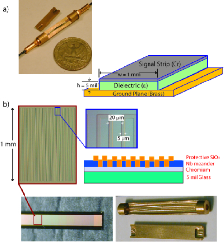
A cross section of the microstrip filters is shown in Fig. 1. The fabrication process is rather straightforward. The chromium is evaporated on 5 mil glass or sapphire wafers. The chromium thickness can be varied to change the resistance per square of the film. The thickness was changed from wafer to wafer depending on the desired parameters and was usually between 10 and 40 nm giving a corresponding resistance of 10 to 110 per square. The Nb meander lines are patterned using electron beam lithography and then etched using a standard fabrication process patel2005 . The meander line has a width of 5 and a pitch of 20 to obtain an inductance of approximately . The meanders were 1 mm wide and as long as 30 mm. In order to achieve these lengths, the 2 mm electron beam fields were stitched together. A 250 nm layer of is deposited on top of the niobium to protect it from scratching and breaking which was a problem in the original batches of filters. The filters are diced to the necessary length and width to reach the desired response and glued to the housings using GE varnish.
Microwaves can propagate in waveguide modes in the filter housing if their frequency exceeds the cutoff frequency. The cutoff frequency for the transverse electric modes , , and transverse magnetic modes, is given by ramo
| (6) |
where W and H are the width and height of the cavity respectively and m and n are indices identifying the number of nodes perpendicular to the direction of propagation, where for either or and for both and . In all of our filter housing designs the height of the cavity is much smaller then the width. For this geometry, Equ. 6 shows the cutoff frequency for all the modes are increased by reducing the height except the which is, independent of this dimension. For the low frequency control lines, the filter housings have dimensions mm and mm, the lowest order waveguide cutoff is GHz and the next lowest mode has a cutoff of GHz. For the high frequency lines, the filter housings have dimensions mm and mm, the waveguide cutoff is GHz and the next lowest mode has a cutoff of GHz.
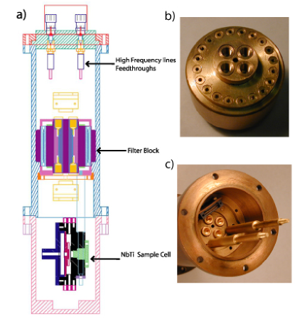
In order to guarantee an optimal thermalization we have housed the microstrip filters in a brass block attached to a vacuum tight sample can that can be anchored at the mixing chamber stage of a dilution refrigerator. As shown in Fig. 2 the sample can consists of two chambers separated by the filter block. The filter block can house up to 20 low low frequency lines and 4 high frequency lines. The device under test is mounted in a NbTi cell that acts as a magnetic shield below its transition temperature around 10K and is located in the bottom chamber of the sample can. Coaxial cables and twisted pairs enter the can through vacuum tight epoxy feedthroughs (Stycast 2850 FT) mounted in the lid. The can is filled with which becomes superfluid at low temperature, providing a uniform thermalization to the microstrip filters and to the qubit chip.
III Testing
We measured the filters attenuation at room and liquid helium temperature. Figure 3 shows the power transmitted through the filter to a detector with a 50 load at room temperature (blue squares) and at 4.2 K (red circles). At high frequencies the rf signal was generated using a HP 83731B synthesized signal generator or a HP 8620C sweep oscillator using a HP 435A power meter and HP 8484A diode power sensor to detect the signal. At lower frequencies, a SRS DS345 synthesized function generator was used to create the signal and a standard oscilloscope was used to measure its rms amplitude. The black triangles show the background of the power sensor. The high and low frequency data sets do not exactly overlap since the power sensor was slightly outside its calibrated range.
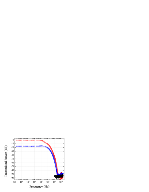
The room temperature data shows 16 dB of attenuation below 10 MHz due to the current primarily traveling though the resistive chromium. The Nb meander line is not superconducting and gives a resistance larger than the chromium. The cutoff, 71 MHz, is consistent with the designed cutoff of the lossy microstrip line. When the Nb goes superconducting the low frequency current is shunted through the meander line and the attenuation is that of the cables alone. The first cutoff at 15 MHz corresponds to the cutoff of the meander line while the second kink is the cutoff of the microstrip. The data shows that after the cutoff the attenuation quickly increases beyond what can be measured using the current setup and stays below the detection threshold to frequencies at least as high as 20 GHz. The Nb meander lines were tested using four point measurements and are superconducting for currents up to 10 mA.
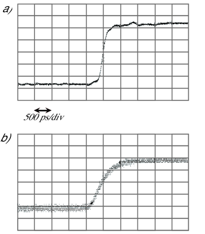
In fig. 4 we show the response of our filters to a DC pulse. As it can be seen from the data, the filters modify the rise time of the pulse from 360ps to 900ps. This is an encouraging result since to test the quantum behavior of a superconductive qubit it is desirable to be able to send pulses with a fast rise time of less than 1ns bennett2007 .
IV Conclusion
The criteria for filters to isolate a qubit from the higher temperature dissipative environment are quite stringent, especially when coupled with the need to get high frequency signals to the qubit for control and readout. We have designed a special type of filter, a lossy transmission line, which cuts off very sharply at the design frequency and has no passbands above the cutof. The lossy microstrip design provides a flexible way to effectively filter many signals over a wide ranges of frequencies. The cutoff and attenuation level of the filters can be controlled by design using the dimensions and the resistivity of the microstrip. These filters are easy to fabricate and install making them a useful tool for measurements of quantum behavior of superconducting devices.
Acknowledgements.
This work was supported in part by NSF and by AFOSR and NSA through a DURINT program.References
- (1) J. Clarke and F.K. Wilhelm, Nature 453, 1031 (2008)
- (2) M.H. Devoret, J.M. Martinis and J. Clarke, Phys. Rev. Lett. 55, 1908 (1985); L. Longobardi, D. Massarotti, G. Rotoli, D. Stornaiuolo, G. Papari, A. Kawakami, G.P. Pepe, A. Barone, and F. Tafuri, Appl. Phys. Lett. 99, 062510 (2011)
- (3) J.M. Kivioja, T.E. Nieminen, J. Claudon, O. Buisson, F.W.J. Hekking, and J.P. Pekola, Phys. Rev. Lett. 94, 247002 (2005); J. Männik, S. Li, W. Qiu, W. Chen, V. Patel, S. Han, and J.E. Lukens, Phys. Rev. B 71, 220509 (2005); L. Longobardi, D. Massarotti, G. Rotoli, D. Stornaiuolo, G. Papari, A. Kawakami, G.P. Pepe, A. Barone, and F. Tafuri, Phys. Rev. B 84, 184504 (2011); L. Longobardi, D. Massarotti, D. Stornaiuolo, L. Galletti, G. Rotoli, F. Lombardi, and F. Tafuri, Phys. Rev. Lett. 109, 050601 (2012)
- (4) D.A. Bennett, L. Longobardi, Vijay Patel, Wei Chen, D. V. Averin, and J. E. Lukens, Quantum Inf. Process., 8, 217 (2009)
- (5) J.M. Martinis, S. Nam, J. Aumentado, and C. Urbina, Phys. Rev. Lett., 89, 117901 (2002)
- (6) Y. Tian, H.F. Yu, H. Deng, G.M. Xue, D.T. Liu, Y.F. Ren, G.H. Chen, D.N. Zheng, X.N. Jing, L. Lu, S.P. Zhao, and S. Han, Rev. Sci. Instrum. 83, 033907 (2012)
- (7) J. Cain, Parasitic inductance of multilayer ceramic capacitors, Tech. Rep. (AVX Corporation)
- (8) Chip monolithic ceramic capacitors catalog, Tech. Rep. (Murata Manufacturing Company)
- (9) S. Ramo, J.R. Whinnery, and T.V. Duzer, Fields and Waves in Communication Electronics (John Wiley and Sons, 1994)
- (10) J.M. Martinis, M.H. Devoret and J. Clarke, Phys. Rev. B 35, 4682 (1987)
- (11) K. Bladh, D. Gunnarsson, E. H rfeld, S. Devi, C. Kristoffersson, B. Smålander, S. Pehrson, T. Claeson, P. Delsing, and M. Taslakov, Rev. Sci. Instrum. 74, 1323 (2003)
- (12) F.P. Milliken, J.R. Rozen, G.A. Keefe, and R.H. Koch, Rev. Sci. Instrum. 78, 024701 (2007)
- (13) A. Lukashenko and A.V. Ustinov, Rev. Sci. Instrum. 79, 014701 (2008)
- (14) A.B. Zorin, Rev. Sci. Instrum. 66, 4296 (1995)
- (15) D. Vion, P.F. Orfila, P. Joyez, D. Esteve, and M.H. Devoret, J. Appl. Phys. 77, 2519 (1995)
- (16) H. le Sueur, and P. Joyez, Rev. Sci. Instrum. 77, 115102 (2006)
- (17) H. Courtois, O. Buisson, J. Chaussy, and B. Pannetier, Rev. Sci. Instrum. 66, 3465 (1995)
- (18) A. Fukushima, A. Sato, A. Iwasa, Y. Nakamura, T. Komatsuzkai, and Y. Sakamoto, IEEE Transactions on Instrumentation and Measurement 46, 289 (1997)
- (19) S. Mandal, T. Bautze, R. Blinder, T. Meunier, L. Saminadayar, and C. Bauerle, Rev. Sci. Instrum. 82, 024704 (2011)
- (20) H. Bluhm, and K.A. Moler, Rev. Sci. Instrum. 79, 014703 (2008)
- (21) D.F. Santavicca, and D.E. Prober, Meas. Sci. Technol. 19, 087001 (2008)
- (22) D.H. Slichter, O. Naaman, and I. Siddiqi, Appl. Phys. Lett. 94, 192508 (2009)
- (23) K. Gupta, R. Garg, and I. Bahl, Microstrip Lines and Slotlines (Artech House Inc., 1979)
- (24) V. Patel, W. Chen, S. Pottorf, and J.E. Lukens, IEEE Transactions on Apllied Superconductivity 15, 117 (2005)
- (25) D.A. Bennett, L. Longobardi, Vijay Patel, Wei Chen, and J. E. Lukens, Supercond. Sci. Technol. 20, S445 (2007)