Spatially resolved quantum plasmon modes in metallic nano-films from first principles
Abstract
Electron energy loss spectroscopy (EELS) can be used to probe plasmon excitations in nanostructured materials with atomic-scale spatial resolution. For structures smaller than a few nanometers quantum effects are expected to be important, limiting the validity of widely used semi-classical response models. Here we present a method to identify and compute spatially resolved plasmon modes from first principles based on a spectral analysis of the dynamical dielectric function. As an example we calculate the plasmon modes of 0.5-4 nm thick Na films and find that they can be classified as (conventional) surface modes, sub-surface modes, and a discrete set of bulk modes resembling standing waves across the film. We find clear effects of both quantum confinement and non-local response. The quantum plasmon modes provide an intuitive picture of collective excitations of confined electron systems and offer a clear interpretation of spatially resolved EELS spectra.
pacs:
73.21.-b,78.20.-e,73.22.Lp,71.45.GmI Introduction
The dielectric properties of a material are to a large extent governed by the collective eigenmodes of its electron system known as plasmons1 . Advances in spectroscopy and materials preparation have recently made it possible to study and control light-matter interactions at the nanometer length scale where particularly the surface plasmons play a key role2 ; 3 . While the ultimate goal of nanoplasmonics as a platform for ultrafast and compact information processing remains a challenge for the future, the unique plasmonic properties of metallic nanostructures have already been utilized in a number of applications including molecular sensors4 ; 5 , photo-catalysis6 and thin-film solar cells7 .
Electron energy loss spectroscopy (EELS) has been widely used to probe plasmon excitations in bulk materials and their surfaces. More recently, the use of highly confined electron beams available in transmission electron microscopes has made it possible to measure the loss spectrum of low-dimensional structures on a sub-nanometer length scale and with eV energy resolution8 . Because the loss spectrum is dominated by the plasmons this technique provides a means for visualising the real-space structure plasmon excitations9 .
All information about the plasmons of a given material is contained in its frequency-dependent dielectric function, , which relates the total potential in the material to the externally applied potential to linear order,
| (1) |
(We have specialized to the case of longitudinal fields which can be represented by scalar potentials). In the widely used Drude model, one neglects the spatial variation of and describes the frequency dependence by a single parameter, the bulk plasmon frequency, where is the average electron density of the material2 . For metal surfaces the Drude model predicts the existence of surface plasmons with frequency . While the Drude model provides a reasonable description of plasmons in simple metal structures in the mesoscopic size regime it fails to account for the dispersion (wave vector dependence) of the plasmon energy in extended systems and predicts a divergent field enhancement at sharp edges. These unphysical results are to some extent remedied by the semi-classical hydrodynamic models which can account for spatial non-locality of and smooth charge density profiles at the metal-vacuum interface2 ; 18 ; 19 . Still, for materials other than the simple metals and for truly nanometer sized structures, predictive modeling of plasmonic properties must be based on a full quantum mechanical description20 ; 21 . The calculation of plasmon energies and EELS spectra of periodic solids from first principles is a well established discipline of computational condensed matter physics22 ; 23 ; 24 ; 25 . However, the application of these powerful methods to systematically explore the real space structure of plasmon excitations at the nanoscale has, to our knowledge, not been achieved previously.
In this paper we present a general method to calculate spatially resolved plasmon modes from first-principles. We apply the method to Na films of a few nanometer thickness where effects of quantum confinement and nonlocal response are expected to be important. The plasmon modes we find can be categorized as surface modes located mainly outside the metal surface, subsurface modes located just below the surface, and bulk modes. Very intuitively, the bulk plasmon modes resemble standing waves with nodes at the film surfaces. However, only plasmons with oscillation periods larger than 10 Å are found as a result of Landau damping which suppresses the strength of plasmon modes with smaller oscillation periods. Finally, we calculate the spatially resolved EELS spectrum of the metal films and show that all its features can be traced to excitation of specific plasmon modes.
II Method
According to Eq. (1), a self-sustained charge density oscillation, , can exist in a material if the related potential, satisfying the Poisson equation (atomic units are used throughout), obeys the equation
| (2) |
In general, this equation cannot be exactly satisfied because the dielectric function will have a finite imaginary part originating from single-particle transitions which will lead to damping of the charge oscillation111We note that exact solutions may be obtained for complex frequencies. However, this requires an analytical continuation of into the complex plane and will not be pursued in the present work. We therefore require only that the real part of vanishes and use the following defining equation for the potential associated with a plasmon mode,
| (3) |
where is a real number. Mathematically, the plasmon modes are thus the eigenfunctions corresponding to purely imaginary eigenvalues of the dielectric function. Physically, they represent the potential associated with self-sustained charge-density oscillations damped by electron-hole pair formations at the rate .
It is instructive to consider the dielectric function in its spectral representation
| (4) |
where the left and right eigenfunctions satisfy the usual orthonormality relation
| (5) |
In the appendix we show that the left and right eigenfunctions are related through Poisson’s equation
| (6) |
and thus correspond to the potential and charge density of the dielectric eigenmode, respectively. Physically, the condition (5) expresses the fact that the different dielectric eigenmodes for a given frequency , are electrodynamically decoupled. The inverse dielectric function, , is obtained by replacing the eigenvalues in Eq. (4) by .
When the imaginary part of the eigenvalue does not vary too much around the plasmon frequency , the condition (3) is equivalent to the condition that
| (7) |
This is the case for most of the plasmon modes of the simple metal films studied in this work. However, for the high energy bulk modes we found that the variation in can shift the local maximum of away from the point where . (The effect can be even stronger of more complex materials with interband transitions.) In such cases the condition (7) rather than (3) should be used to define the plasmon energy. Importantly, however, the eigen functions do not change significantly when is varied between the frequencies given by the two criteria and thus the spatial form of the plasmon remains well defined.
In the case of metallic films where the in-plane variation of and can be assumed to have the forms and , respectively, Eq. (3) can be written
| (8) |
We stress that despite the atomic variation in the potential we have found that local field effects are negligible within the plane justifying this assumption.
All the calculations were performed with the electronic structure code GPAW28 ; 29 using the Atomic Simulation Environment30 . The Na films were modeled in a supercell with periodic boundary conditions imposed in all directions. The minimal Na unit cell was used in the plane of the film and 30 Å of vacuum was included in the direction perpendicular to the film to separate the periodic images. The single-particle wave functions and energies were computed on a real space grid with a grid spacing 0.18 Å and the Brillouin zone was sampled by 64x64 -points. The LDA functional was used for exchange and correlation. The non-interacting density response function, , was calculated from the DFT single-particle states using a 50 eV energy cutoff for the plane wave basis and including states up to 15 eV above the Fermi level. The frequency-dependence of the dielectric function was sampled on the real frequency axis using a grid from 0 to 20 eV with a 0.1 eV spacing. We checked that our results were converged with respect to all the parameters of the calculation. The microscopic dielectric function was calculated from using the random phase approximation (RPA). We note in passing that this DFT-RPA level of theory yields highly accurate bulk and surface plasmon energies (within a few tenths on an electron volt) of the simple metals25 .
To obtain the plasmon modes, the dielectric function is diagonalized in a plane-wave basis on each point of a uniform frequency grid. To simulate an isolated film, the obtained eigenmode potentials were corrected to remove the effect of interactions with films in the other supercells, i.e. the periodic boundary conditions from the DFT calculation (this is most important for small vectors). In general the eigenmodes were found to be complex valued reflecting the spatial variation in the phase of the plasmon potential. This phase variation is, however, rather weak for the present system, and by a suitable choice of the overall phase the modes can be made almost real . For this reason only the real part is shown in Figs. 1 and 3.
III Results
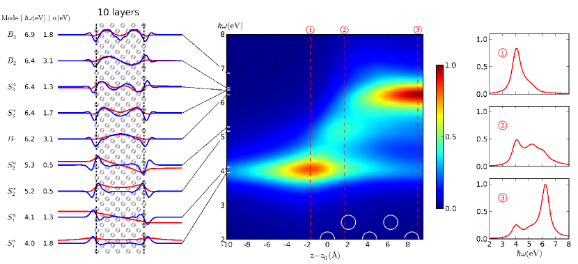
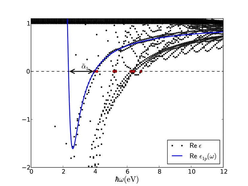
In Fig. 1(a) we show the plasmon modes (red) and corresponding charge densities (blue) obtained for a 10 atom thick Na film terminated by (100) surfaces. Fig. 2 shows the real part of the eigenvalues of for the 10 layer film. The red dots indicate the plasmon frequencies, , where the real part of an eigenvalue crosses the real axis from below. Note that the point where an eigenvalue crosses the real axis from above corresponds roughly to the energy of the individual single-particle transitions contributing to the plasmon state. Thus the distance between the two crossing points, , represents the Coulombic restoring force of the plasma oscillation. The eigenfunctions of corresponding to the indicated eigenvalues are the plasmon modes shown in Fig. 1. The energies and strengths, , of the plasmon modes are listed to the left. The strength is determined by fitting a single-pole model
| (9) |
to the value and slope of the relevant eigenvalue branch of at the point , see Fig. 2.
Returning to Fig. 1, we see that the lowest lying plasmon modes (S1) are the symmetric and anti-symmetric surface plasmons also predicted by the classical Drude model. The two sets of modes denoted S2 and S3 are also localized at the surface, although they penetrate more into the bulk, and we therefore refer to them as subsurface modes. The subsurface character of the S3 mode is perhaps more evident for the 20 layer film where it is more clearly separated from the bulk modes, see Fig. 4. Experimental loss spectra of simple metal surfaces have shown a small peak between the surface and bulk peaks which was assigned to a subsurface plasmon (in that work denoted multipole surface mode)17 . Such a peak at intermediate energies was also observed in a previous RPA calculation for a jellium surface26 . However, the complete analysis of the plasmons modes presented here shows that more than one subsurface mode exists.
The bulk plasmons (B) occur at higher energies and resemble standing waves across the film. The fact that only a discrete set of bulk modes are observed is clearly a result of confinement of the electron gas which requires the density to vanish at the boundaries of the film. The reason only a finite number of modes are found is that the damping of the modes due to single-particle transitions increases for smaller oscillation periods, i.e. larger wave number. Consequently, the strength of the bulk plasmons decreases with increasing wave number until the point where the real part of does not cross the real axis. This is evident in Fig. 2 where a series of local minima in the eigenvalue spectrum can be seen at higher frequencies. For all the films, the highest lying bulk mode has a wave number around 0.5 Å-1. This is very close to the threshold where becomes positive for all in bulk Na.
As already mentioned, the main mechanism of energy loss of fast electrons propagating through a material is via excitation of plasmons. In general, the energy dissipated to the electron system due to an applied potential of the form , is
| (10) |
Here is the imaginary part of the density response function, . In the case of a fast electron, the external potential is simply that of a point charge moving at constant velocity. We have calculated the loss function for high energy electron beams directed along lines parallel to the film. The resulting EELS spectrum is seen in the middle panel of Fig. 1. It is clear that the loss spectrum is completely dominated by three types of excitations corresponding to the surface, subsurface, and bulk plasmon modes shown to the left. The intensity of the subsurface modes is rather weak in agreement with the low strength () of these modes.
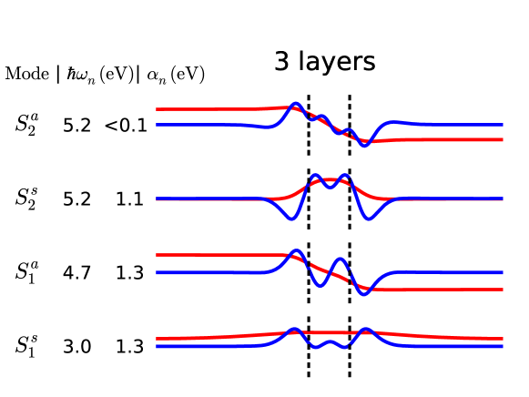
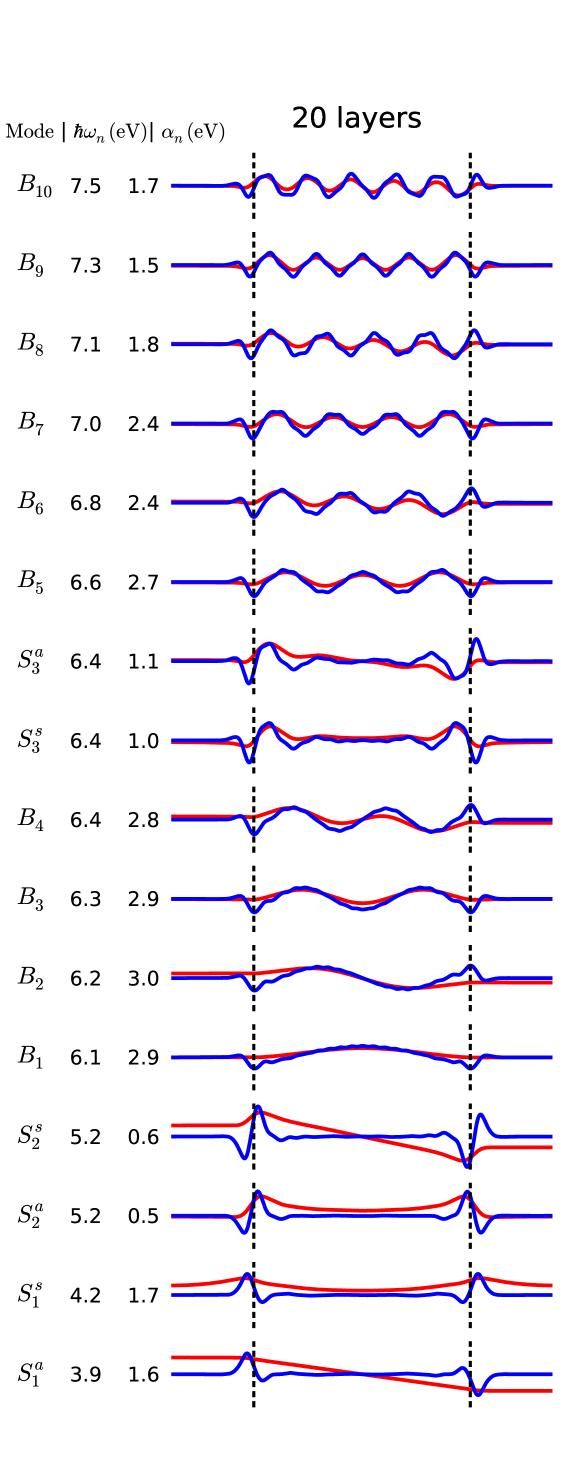
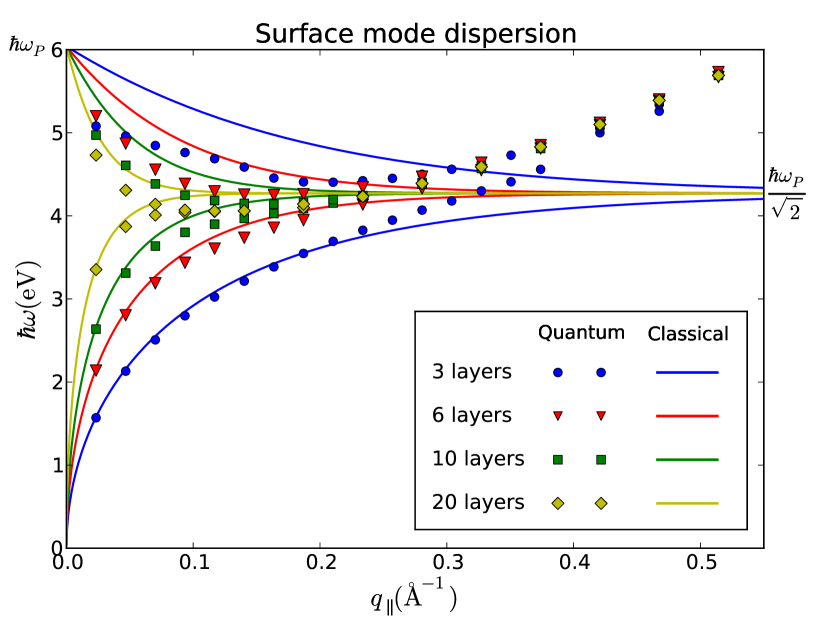
Fig. 5 shows all the energies of the symmetric and anti-symmetric surface plasmons (subsurface plasmons not included) found for four different film thicknesses as a function of the in-plane wave vector, details_fig4 . The full curves are the classical Drude results for a 2D metal film with the electron density of Na. For small the agreement with the classical result is striking for the symmetric mode. On the other hand, the quantum results for the anti-symmetric mode are significantly red shifted compared to the Drude result with deviations up to 1 eV for the thinnest film. For large the quantum plasmons show a dispersion whereas the classical result approaches the asymptotic value . This failure of the classical model is due to the neglect of the spatial non-locality of , i.e. the -dependence.
We note that when exchange-correlation effects are included through the adiabatic local density approximation (ALDA) kernel, a larger deviation from the classical model is observed. In particular the anti-symmetric mode is shifted even further down for small . A similar behavior, i.e. downshift of plasmon energies, is observed for simple metal bulk systems where the ALDA also predicts a negative dispersion for small 2 . The spatial form of the plasmon modes obtained with the ALDA is, however, identical to those obtained at the RPA level.
In Fig. 6 we show the same data as shown in Fig. 5 but with the plasmon energy plotted relative to the dimensionless parameter , where is the film thickness. When plotted in this way all the classical dispersions fall on the same universal curve. In the regime , it is clear that the quantum results for the anti-symmetric mode are not converged to the classical result even for the thickest slab.
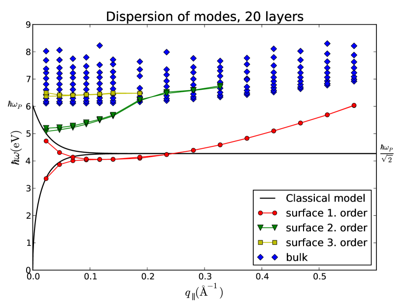
In Fig. 7 we present the dispersion of all plasmon modes (conventional surface, sub-surface, and bulk modes) for the 20 layer film. The bulk modes show a weak dispersion. The energy offset between the different bulk modes arises from the different wave lenght of the plasmons in the normal direction. The energy of the lowest bulk mode (B1) in the limit is eV higher than the bulk value of . This small deviation is due to the finite wave length of the plasmon on the direction perpendicular to the film and this indicates that quantum size effects have a very small influence on the bulk modes of the 20 layer film.
The first sub-surface modes (green color) follows a dispersion until around Å-1 where it enters the bulk mode energy range. From this point the dispersion of the sub-surface mode is reduced and follows that of the bulk modes. The dispersion of the second sub-surface modes (yellow color) is very similar to the bulk dispersion. The second sub-surface mode is rather weak and for Å-1 its eigenvalue, , does not cross the real axis at any frequency. For both subsurface modes the splitting between the symmetric and anti-symmetric modes is rather small. We ascribe this to the weaker strength of the electric field associated with the subsurface mode compared to the conventional surface mode: While the charge distribution, associated with the latter has monopole character in the direction perpendicular to the film, the subsurface modes have dipole character, see Fig. 4.

IV Conclusion
We have introduced a method for calculating spatially resolved plasmon modes in nanostructured materials from first principles. For the case of 2D Na films of thickness 0.5-4 nm we found that the modes could be classified as either surface modes, subsurface modes or bulk modes. In contrast to previous studies, the direct computation of eigenmodes revealed that several subsurface modes can exist at the surface of simple metals. We found clear effects of quantum confinement on the surface plasmon energies. In particular, the anti-symmetric surface mode of the thinner films were significantly red shifted compared to the classical Drude result. Finally, it was demonstrated how the different features in the calculated spatially resolved EELS spectrum of the metal films could be unambiguously ascribed to the excitation of specific plasmon modes. Apart from providing an intuitive and visual picture of the collective excitations of a nanostructure, the spatially resolved plasmon modes should be useful as a basis for the construction of simple models for the full non-local dielectric function.
V Acknowledgements
K. S. T. acknowledges support from the Danish Research Council’s Sapere Aude Program. The Center for Nanostructured Graphene CNG is sponsored by the Danish National Research Foundation. Support from The Catalysis for Sustainable Energy (CASE) initiative and the Center of Nanostructuring for Efficient Energy Conversion (CNEEC) at Stanford University, an Energy Frontier Research Center funded by the US Department of Energy, Office of Science, Office of Basic Energy Sciences under Grant no. DE-SC0001060, is also acknowledged.
Appendix A Spectral representation of
Let denote the eigenfunctions of the dielectric function,
| (11) |
(we have suppressed the dependence for notational simplicity). Since is a non-hermitian operator, the eigenvalues are complex and the eigenfunctions are non-orthogonal. In this case the spectral representation takes the form
| (12) |
The set is the dual basis of and satisfies
| (13) |
From the spectral representation it follows directly that
| (14) |
In the following we show that the dielectric eigenfunction and its dual function constitute a potential-density pair, i.e.
| (15) |
Within the RPA, the dielectric function is related to the non-interacting polarization function, , by
| (16) |
where is the Coulomb interaction, . Exploiting that, under time reversal symmetry , we have
| (17) |
We now make the ansatz and evaluate
| (18) | |||||
| (19) | |||||
| (20) |
which concludes the proof.
References
- (1) D. Bohm and D. Pines, Phys. Rev. 92, 609-625 (1953)
- (2) J. M. Pitarke, V. M Silkin, E. V. Chulkov, and P. M. Echenique, Rep. Prog. Phys. 70, 1-87 (2007).
- (3) K. A. Willets and R. P. Van Duyne, Annu. Rev. Phys. Chem. 58, 267-297 (2007)
- (4) K. Kneipp, Y. Wang, H. Kneipp, L. T. Perelman, I. Itzkan, R. R. Dasari, and M. S. Feld, Phys. Rev. Lett. 78, 1667 (1997).
- (5) E. M. Larsson, C. Langhammer, I. Zori, and B. Kasemo, Science 326, 1091 (2009).
- (6) T. Hirakawa and P. V. Kamat, J. Am. Chem. Soc. 127, 3928
- (7) H. A. Atwater and A. Polman, Nature Materials 9, 205 (2010).
- (8) F. J. Garcia de Abajo, Rev. Mod. Phys. 82, 209 (2010).
- (9) B. S. Guiton, V. Iberi, S. Li, D. N. Leonard, C. M. Parish, P. G. Kotula, M. Varela, G. C. Schatz, S. J. Pennycook, and J. P. Camden, Nano Lett. 11, 3482 (2011); O. Nicoletti, M. Wubs, N. A. Mortensen, W. Sigle, P. A. van Aken, and P. A. Midgley, Optics Express 19, 15371 (2011); W. Zhou, J. Lee, J. Nanda, S. T. Pantelides, S. J. Pennycook, and J. C. Idrobo, Nature Nanotechnology 7, 161 (2012); J. Nelayah, M. Kociak, O. Stèphan, F. J. Garcia de Abajo, M. Tencè, L. Henrard, D. Taverna, I. Pastoriza-Santos, L. M. Liz-Marzàn, and C. Colliex, Nature Physics 3, 348 (2007); A. L. Koh, A. I. Fernandez-Dominguez, D. W. McComb, S. A. Maier, and J. K. W. Yang, Nano Lett. 11, 1323 (2011); M. Bosman, V. J. Keast, M. Watanabe, A. I. Maaroof, and M. B. Cortie, Nanotechnology 18, 165505 (2007); M. N’Gom, S. Li, G. Schatz, R. Erni, A. Agarwal, N. Kotov, and T. B. Norris, Phys. Rev. B 80, 113411 (2009); J. A. Scholl, A. L. Koh, and J. A. Dionne, Nature 483, 421 (2012).
- (10) K. -D. Tsuei, E.W. Plummer, A. Liebsch, E. Pehlke, K. Kempa and P. Bakshi, Surf. Science 247, 302-326 (1991).
- (11) C. David and F. J. Garcia de Abajo, J. Phys. Chem. C 115, 19470 (2011).
- (12) S. Raza, G. Toscano, A. P. Jauho, M. Wubs, and N. A. Mortensen, Phys. Rev. B 84, 121412(R) (2011).
- (13) T. Sokusin, A. Manjavacas, and F. J. Garcia de Abajo, ACS Nano 6, 1766-1775 (2012).
- (14) J. Yan, Z. Yuan, and S. W. Gao, Phys. Rev. Lett. 98, 216602 (2007).
- (15) G. Onida, L. Reining, and A. Rubio, Rev. Mod. Phys. 74, 601-659 (2002).
- (16) C. Kramberger, R. Hambach, C. Giorgetti, M. H. Rümmeli, M. Knupfer, J. Fink, B. Büchner, L. Reining, E. Einarsson, S. Maruyama, F. Sottile, K. Hannewald, V. Olevano, A. G. Marinopoulos, and T. Pichler, Phys. Rev. Lett. 100, 196803 (2008).
- (17) A. Marini, R. Del Sole, and G. Onida, Phys. Rev. B 66, 115101 (2002).
- (18) J. Yan, K. W. Jacobsen, and K. S. Thygesen, Phys. Rev. B 84, 235430 (2011)
- (19) In the case of Ag films (results will be published elsewhere) we have found that the coupling to interband transitions can shift the peak of away from the point where . Importantly, however, the corresponding eigen function do not change significantly when is varied between the frequencies given by the two criteria and thus the spatial form of the plasmon remains well defined.
- (20) J. Yan, J. J. Mortensen, K. W. Jacobsen, and K. S. Thygesen, Phys. Rev. B 83, 245122 (2011).
- (21) J. Enkovaara, C. Rostgaard, J. J. Mortensen, J. Chen, M. Dulak, L. Ferrighi, J. Gavnholt, C. Glinsvad, V. Haikola, H. A. Hansen, H. H. Kristoffersen, M. Kuisma, A. H. Larsen, L. Lehtovaara, M. Ljungberg, O. Lopez-Acevedo, P. G. Moses, J. Ojanen, T. Olsen, V. Petzold, N. A. Romero, J. Stausholm-Møller, M. Strange, G. A. Tritsaris, M. Vanin, M. Walter, B. Hammer, H. Häkkinen, G. K. H. Madsen, R. M. Nieminen, J. K. Nørskov, M. Puska, T. T. Rantala, J. Schiøtz, K. S. Thygesen and K. W. Jacobsen, J. Phys. Condens. Matter 22, 253202 (2010).
- (22) S. R. Bahn and K. W. Jacobsen, Comput. Sci. Eng., Vol. 4, 56-66 (2002).
- (23) W. L. Schaich and J. F. Dobson, Phys. Rev. B 49, 14700 (1994)
- (24) To obtain the dispersion of the surface plasmons (Fig. 4) of an isolated film, the calculated plasmon energies were extrapolated to the limit of infinite distance between the repeated films using a classical model for the plasmon energies in an infinite array of films. The model is a straightforward generalization of the results in Ref. 27
- (25) R. A. Ferrell, Phys. Rev. 111, 1214 (1958).