A quantum phase transition from triangular to stripe charge order in NbSe2
Abstract
The competition between proximate electronic phases produces a complex phenomenology in strongly correlated systems. In particular, fluctuations associated with periodic charge or spin modulations, known as density waves, may lead to exotic superconductivity in several correlated materials. However, density waves have been difficult to isolate in the presence of chemical disorder, and the suspected causal link between competing density wave orders and high temperature superconductivity is not understood. Here we use scanning tunneling microscopy to image a previously unknown unidirectional (stripe) charge density wave (CDW) smoothly interfacing with the familiar tri-directional (triangular) CDW on the surface of the stoichiometric superconductor NbSe2. Our low temperature measurements rule out thermal fluctuations, and point to local strain as the tuning parameter for this quantum phase transition. We use this discovery to resolve two longstanding debates about the anomalous spectroscopic gap and the role of Fermi surface nesting in the CDW phase of NbSe2. Our results highlight the importance of local strain in governing phase transitions and competing phenomena, and suggest a new direction of inquiry for resolving similarly longstanding debates in cuprate superconductors and other strongly correlated materials.
A Introduction
While a classical phase transition separates two states of matter at different temperatures, two ordered ground states of a material at zero temperature are separated by a quantum critical point (QCP). The competition between proximate ordered phases near the QCP can dramatically influence a large region of the phase diagramSachdev (2000). While the fluctuations from competing quantum states lead to exotic physics even at higher temperatures, low temperature studies of these states can lead to a better understanding of the root of the competition. Density waves - charge or spin ordered states of collective origin driven by instabilities of the Fermi surface (FS) - exist in close proximity to superconductivity (SC) in several classes of correlated materialsNorman et al. (2005); Johnston (2010); Jérome and Schulz (2002), and various proposals have recently emerged to study their interplay in the presence of strong inhomogeneity in these systemsKivelson et al. (2003). In this light, it is surprising that charge density waves (CDWs) are not fully understood even in the weakly correlated and stoichiometric transition metal dichalcogenides (TMDCs). While a classic CDW arises from strong FS nesting, resulting in a sharply peaked susceptibility and a Kohn anomaly at the CDW wavevector, the quasi-2D TMDCs are known to deviate from this pictureJohannes et al. (2006).
-NbSe2 is a layered TMDC which has generated much recent interestSuderow et al. (2005); Kiss et al. (2007); Feng et al. (2012) as a model system for understanding the interplay of the CDW and SC phases which onset at and respectivelyMoncton et al. (1975); Wilson et al. (2001). Despite extensive studyKiss et al. (2007); Borisenko et al. (2009); Mialitsin (2010); Weber et al. (2011); Rahn et al. (2012), several key facts about its familiar tri-directional () CDW remain unresolved, including the role of FS nesting in determining its wavevector , and the magnitude of the spectral gap and its role in the energetics of the transition. First, angle-resolved photoemission (ARPES) studies have been unable to uniquely identify -nested FS regions in -NbSe2Kiss et al. (2007); Borisenko et al. (2009); Rahn et al. (2012); Straub et al. (1999); Rossnagel et al. (2001); Valla et al. (2004); Shen et al. (2008). Meanwhile, recent studies indicate a broadly peaked susceptibility and a soft phonon over a range of wavevectors around Johannes et al. (2006); Weber et al. (2011); Rahn et al. (2012), suggesting instead that the -dependence of the electron-phonon coupling could play an important role in driving the transition. Second, kinks in tunneling spectra at (), historically identified as gap edges, correspond to an anomalously large energy scale for the corresponding )Hess et al. (1991), while recent ARPES studies indicate a much smaller gapBorisenko et al. (2009); Rahn et al. (2012).
Our discovery, by low-temperature scanning tunneling microscopy (STM), of a CDW with distinct wavelength and tunneling spectra from the CDW, in conjunction with band structure calculations, allows us to resolve both longstanding questions of the wavevector and the gap. First, the distinct wavelengths demonstrate that FS nesting plays a negligible role in setting their magnitude. Second, the distinct tunneling spectra of the CDW region help us disentangle the CDW spectra to expose a particle-hole asymmetric gap, riding on top of a strong inelastic background.
B Results

Fig. 1A shows a topographic image of a locally commensurate ) CDW. Its microscopic nature is confirmed by the existence of a secondary CDW peak in the Fourier Transform (FT) in Fig. 1B, in contrast to bulk measurementsFeng et al. (2012). Phase slips result in an overall periodicity of , corresponding to , where is the Bragg vectorMoncton et al. (1975); Feng et al. (2012); McMillan (1976). Our primary experimental discovery is shown in Fig. 2A, where regions of unidirectional () CDW with unique wavevector along a single direction form an atomically smooth interface with the CDW. The absence of atomic lattice discontinuities rules out the possibility of a NbSe2 polytype interfaceWang et al. (2009). While other TMDCs are known to exhibit a thermally induced triclinic CDW state that varies with doping near McMillan (1976); Bando et al. (1997), no such anisotropy has been reported in -NbSe2. Moreover, our observations are at temperatures , where thermal fluctuations are insignificant, implying that the CDW is a distinct quantum phase.
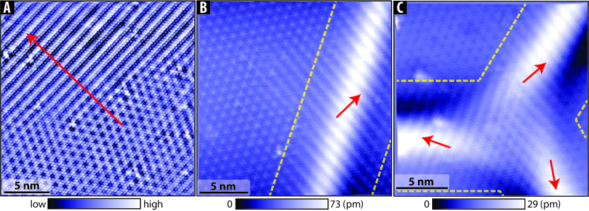
The CDW regions take the form of elevated topographic ribbons, exemplified in Fig. 2B-C, suggesting a strain-induced phase (§ SI II). The observation of -junctions between ribbons with differently oriented rules out extrinsic uniaxial strain and suggests instead locally varying strain, perhaps due to underlying defects causing nanoscale buckling of the top few atomic layers. From a survey of several ribbons, we place upper bounds of on the vertical strain and on the lateral strain (see § SI II).
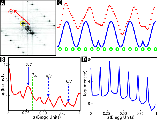
Fig. 3A-B show the dominant Fourier peak for the modulation, , corresponding to a wavelength, . No similar periodicity or rich harmonic structure has thus far been reported in any TMDC systemWilson et al. (2001). We develop a phenomenological understanding of the harmonic structure following McMillan’s Landau theoryMcMillan (1975, 1976). Rather than a uniform charge modulation, the system could lower its energy by locking the charge modulation to the lattice with periodicity. This would require compensation by a one atom phase slip every two oscillations, corresponding to a discommensuration, as shown in Fig. 3CMcMillan (1976). The resulting harmonic structure shown in Fig. 3D reproduces all observed peak positions. Moreover, the rich harmonic content we observe is another indication of the strong coupling of the electronic modulation to the lattice. An even better agreement with relative peak heights could be obtained by considering spatial variations in the order parameter amplitudeMcMillan (1976).
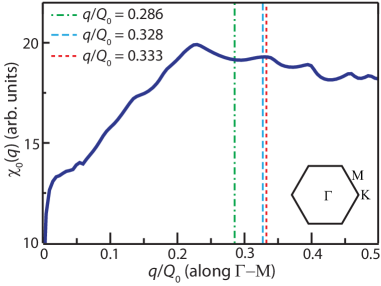
The stark contrast between our observation of two CDW wavevectors and of same orientation but difference in magnitude, and the recent X-ray measurements reported by Feng et al.Feng et al. (2012), provides strong evidence against FS nesting at one particular wavevector as a driving force for either CDW. While our wavevector difference arose from moderate anisotropic strain (up to in-plane), Feng et al. applied hydrostatic pressure sufficient to induce in-plane lattice distortions up to , yet observed no measurable deviation of the CDW wavevector from Feng et al. (2012). The observed insensitivity of to hydrostatic pressure would clearly indicate that the FS does not qualitatively change in the presence of even relatively large lattice distortions, and would thus rule out a change in the FS as the source of our observed wavevector difference. Furthermore, consistent with our experiment and with previous calculationsJohannes et al. (2006); Weber et al. (2011); Rahn et al. (2012), we find no sharp peak in the susceptibility (Fig. 4) computed from our modeled band structure (§ SI III). Therefore, our observations and calculations both indicate that the FS can play only a minor role in determining CDW wavevectors in NbSe2. This highlights the key role that the -dependence of alternative mechanisms such as electron-phonon coupling may play in driving the transition, and particularly the manner in which these mechanisms may be influenced by local strain.
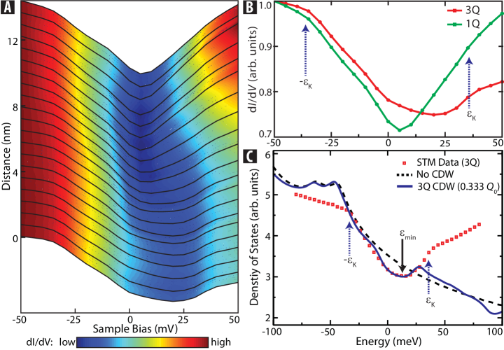
The two CDW regions display quite different tunneling spectra, as shown in Fig. 5A-B. We employ a fit to the NbSe2 band structure (§ SI III), and impose a CDW wavevector , gap , and broadening parameter , to calculate the density of states (DOS), in Fig. 5C (§ SI IV). For the CDW state the measured spectrum, proportional to the DOS, is best reproduced using (the observed local CDW periodicity), (which has not been previously apparent from direct observations by spectroscopic techniques), and . The calculations capture the overall shape, width, and center of the gap structure within 30 mV of (§ SI IV). The fact that is offset from should be unsurprising for a quasi-2D systemNorman et al. (2007), but had not been understood or observed in NbSe2 until now, due to limitations of spectroscopic techniques which are sensitive to filled states onlyBorisenko et al. (2009).
We disentangle the CDW gap from other effects in the spectra through a comparison with the spectra in Fig. 5B. These -shaped spectra resemble the linear tunneling conductance background historically attributed to the inelastic coupling of tunneling electrons to a flat bosonic spectrumKirtley et al. (1992). That this background is much stronger in the region, obscuring band structure effects, is likely a strain-induced phenomenon, which may be related to the buckling and associated decoupling of the topmost layers in the region. Meanwhile, present in both and spectra (thus unlikely to be associated with these different CDWs), yet absent in calculations (thus unlikely to be a band structure effect), are the kinks, previously and mistakenly identified as the CDW gapHess et al. (1991). We universally observe the kinks even well above , which further demonstrates their lack of bearing on the CDW phase (§ SI IV). ARPES studies observe a prominent band structure kink at a similar energy in the Se -pocketValla et al. (2004); Rahn et al. (2012), attributed to coupling to an optical phononMialitsin (2010). We therefore conclude that this self-energy effect is responsible for the kinks in the tunneling spectra as well. The discrepancy between the data and band structure calculations above in Fig. 5C can thus be attributed to the inelastic tunneling background and self-energy effects.
C Discussions
We therefore resolve a longstanding debate about the anomalous CDW gap magnitude reported by STM measurementsHess et al. (1991), and caution that not all -symmetric kinks in tunneling spectra are associated with order (e.g. density wave or superconducting gaps). On the contrary, we emphasize that the true CDW signature in NbSe2 is offset from , which has confused an active research community for two decades, and has been disentangled now only by a combination of spatially resolved filled and empty state spectroscopy of a proximate () phase, and band structure calculationsNorman et al. (2007). This emphasizes the need for full experimental exploration of proximate phases in other pertinent materials, combined with quantitative modeling. We further suggest that controlled local strain, through epitaxy or intentional defects, may be a useful tuning parameter to access the necessary proximate phases for comparison.
Beyond providing new insight into the nature of the CDW in NbSe2, our work motivates the utility of the interface in NbSe2 as a platform to explore competing quantum phases in the weakly correlated limit, as a step towards understanding them in strongly correlated systems. In the Landau picture of CDWsMcMillan (1975), a quantum phase transition between and states can arise by tuning the coefficient of the interaction term between the three inequivalent CDW propagation directions (though in our case, the magnitude of differs between the two states). In NbSe2, even at low temperatures , where the amplitude of the order parameter is already large, moderate strain is seen to have a strong influence, indicating that the system is intrinsically close to the QCP separating these states. We note that a related phase transition between the observed CDW phase and a ‘hidden’ phase has been suggested, but not directly visualized, in the rare-earth tritelluridesYao et al. (2006); Ru et al. (2008).
Our discovery provides a new perspective on the role of density wave order in complex systems. First, our resolution of two longstanding debates about NbSe2 puts this much-studied material on firmer footing as a well-understood model system for CDW studies and competing ground states in superconductors. We have disentangled the true CDW gap, and clarified that FS nesting plays a minor role in determining the CDW wavevectors in this material, thereby highlighting the role of other mechanisms in driving the transition. Second, our revelation of a particle-hole asymmetric CDW gap emphasizes the limitations of filled-state-only probes, e.g. ARPES, for investigating phases other than SC - which is unambiguously particle-hole symmetric. Full spectral probes such as STM, in combination with quantitative calculations, are necessary to understand the competition between SC and particle-hole asymmetric phases. Third, our observation of the local effect of even moderate strain in driving a quantum phase transition calls for a reinvestigation of possible phase inhomogeneity in other strongly correlated systems, where larger strain may occurSlezak et al. (2008); Chu et al. (2010).
In the cuprate superconductors, an analogous phase boundary between unidirectional () charge ‘stripes’ and bidirectional () ‘checkerboard’ has been predictedRobertson et al. (2006); Del Maestro et al. (2006). The introduction of quenched disorder results in discommensurations in the phase and disordered orientational order in the phase, making them hard to distinguish - especially in the cuprate BSCCO, thought to be in proximity to the phase boundaryRobertson et al. (2006); Del Maestro et al. (2006). Recent STM studies of the charge order in BSCCO have had conflicting interpretations, with independent suggestions of fluctuating and orderWise et al. (2008); Parker et al. (2010). However, the influence of strain, from the supermodulation lattice buckling, or from randomly distributed dopants, is seldom accounted for. Previous studies have shown that both these strain phenomena correlate with nanoscale electronic inhomogeneitySlezak et al. (2008); Zeljkovic et al. (2012). A possible explanation is local stabilization of the state, producing and interfaces with spectral differences, analogous to Fig. 2 and Fig. 5A-B. While the presence of strong disorder (up to strain variations on a nanometer length scaleSlezak et al. (2008)) complicates the interpretations in BSCCO, we stress the importance of isolating and modeling strain effects for better understanding and control of the phase transitions in cuprates. Finally, the microscopic visualization of the role of strain in stabilizing new order suggests a controlled route towards engineering novel quantum phases and interfaces and studying symmetry breaking in strongly correlated materials. In this regard, we suggest a connection to the emerging importance of strain as a route to high- superconductivity in novel iron-based materialsSaha et al. (2012); Wang et al. (2012).
D Methods
STM Experiments.
Measurements were performed using a home-built STM at temperatures between K. Magnetic fields of up to were used to suppress the superconducting state as needed. Single crystals of -NbSe2 were cleaved in situ in cryogenic ultrahigh-vacuum and inserted into the STM. A mechanically cut PtIr tip, cleaned by field emission and characterized on gold, was used for the measurements. Spectroscopy data were acquired using a lock-in technique at 1.115 kHz. The topographic and spectroscopic signatures of the ribbons have been verified with several tips.
Band Structure and DOS Calculations.
The band structure of -NbSe2 close to consists of two Nb derived bands and one Se ‘pancake’-shaped hole pocketJohannes et al. (2006). The Nb bands are modeled using a tight-binding fit to the observed ARPES band structureRahn et al. (2012), and the Se pocket is approximated by a simple quadratic form to fit LDA calculationsJohannes et al. (2006) (details in § SI III). Using all three bands, the DOS in the presence of a CDW is calculated by imposing a constant coupling between electronic states connected by any one of the three -vectors. The strength of the coupling is taken as a free parameter in the reproduction of the experimentally observed DOS, and the size of is allowed to vary slightly around the observed value of (details in § SI IV).
Acknowledgements.
We are grateful to Patrick Lee and Steve Kivelson for insightful discussions and to Wilfried Krüger, Lutz Kipp and Daniel Walkup for useful experimental inputs. This work was supported by NSF DMR-0847433 and the New York Community Trust - George Merck Fund (Harvard), DOE, Office of Science, under Contract No. DE-AC02-06CH11357 (Argonne) and DFG via SFB 855 (Kiel). In addition, we acknowledge funding from A*STAR, Singapore (A.S.) and NSERC, Canada (M.M.Y.).
Author Contributions.
A.S., M.M.Y. and Y.H. performed STM experiments, and A.S. led the data analysis with contributions from M.M.Y. D.J.R. and K.R. grew and characterized samples. J.v.W., K.R. and M.R.N. performed calculations. A.S. wrote the main manuscript with theoretical sections written by J.v.W. E.W.H., K.R., M.R.N. and J.E.H. advised the work and edited the manuscript.
Author Information.
The authors declare no competing financial interests. Correspondence and requests for materials should be addressed to A.S. (anjan@physics.harvard.edu) and J.E.H. (jhoffman@physics.harvard.edu).
References
- Sachdev (2000) S. Sachdev, Science 288, 475 (2000).
- Norman et al. (2005) M. R. Norman, D. Pines, and C. Kallin, Advances in Physics 54, 715 (2005).
- Johnston (2010) D. C. Johnston, Advances in Physics 59, 803 (2010).
- Jérome and Schulz (2002) D. Jérome and H. J. Schulz, Advances in Physics 51, 293 (2002).
- Kivelson et al. (2003) S. A. Kivelson, I. P. Bindloss, V. Oganesyan, J. M. Tranquada, A. Kapitulnik, and C. Howald, Reviews of Modern Physics 75, 1201 (2003).
- Johannes et al. (2006) M. D. Johannes, I. I. Mazin, and C. A. Howells, Physical Review B 73, 205102 (2006).
- Suderow et al. (2005) H. Suderow, V. G. Tissen, J. P. Brison, J. L. Martínez, and S. Vieira, Physical Review Letters 95, 117006 (2005).
- Kiss et al. (2007) T. Kiss, T. Yokoya, A. Chainani, S. Shin, T. Hanaguri, M. Nohara, and H. Takagi, Nature Physics 3, 720 (2007).
- Feng et al. (2012) Y. Feng, J. Wang, R. Jaramillo, J. van Wezel, S. Haravifard, G. Srajer, Y. Liu, Z. A. Xu, P. B. Littlewood, and T. F. Rosenbaum, Proceedings of the National Academy of Sciences 109, 7224 (2012).
- Moncton et al. (1975) D. E. Moncton, J. D. Axe, and F. J. DiSalvo, Physical Review Letters 34, 734 (1975).
- Wilson et al. (2001) J. A. Wilson, F. J. D. Salvo, and S. Mahajan, Advances in Physics 50, 1171 (2001).
- Borisenko et al. (2009) S. V. Borisenko, A. A. Kordyuk, V. B. Zabolotnyy, D. S. Inosov, D. V. Evtushinsky, B. Büchner, A. N. Yaresko, A. Varykhalov, R. Follath, W. Eberhardt, et al., Physical Review Letters 102, 166402 (2009).
- Mialitsin (2010) A. Mialitsin, Phd, Rutgers University (2010).
- Weber et al. (2011) F. Weber, S. Rosenkranz, J.-P. Castellan, R. Osborn, R. Hott, R. Heid, K.-P. Bohnen, T. Egami, A. Said, and D. Reznik, Physical Review Letters 107, 107403 (2011).
- Rahn et al. (2012) D. J. Rahn, S. Hellmann, M. Kalläne, C. Sohrt, T. K. Kim, L. Kipp, and K. Rossnagel, Physical Review B 85, 224532 (2012).
- Straub et al. (1999) T. Straub, T. Finteis, R. Claessen, P. Steiner, S. Hüfner, P. Blaha, C. S. Oglesby, and E. Bucher, Physical Review Letters 82, 4504 (1999).
- Rossnagel et al. (2001) K. Rossnagel, O. Seifarth, L. Kipp, M. Skibowski, D. Voß, P. Krüger, A. Mazur, and J. Pollmann, Physical Review B 64, 235119 (2001).
- Valla et al. (2004) T. Valla, A. V. Fedorov, P. D. Johnson, P.-A. Glans, C. McGuinness, K. Smith, E. Y. Andrei, and H. Berger, Physical Review Letters 92, 086401 (2004).
- Shen et al. (2008) D. W. Shen, Y. Zhang, L. X. Yang, J. Wei, H. W. Ou, J. K. Dong, B. P. Xie, C. He, J. F. Zhao, B. Zhou, et al., Physical Review Letters 101, 226406 (2008).
- Hess et al. (1991) H. F. Hess, R. B. Robinson, and J. V. Waszczak, Physica B: Condensed Matter 169, 422 (1991).
- McMillan (1976) W. L. McMillan, Physical Review B 14, 1496 (1976).
- Wang et al. (2009) H. Wang, J. Lee, M. Dreyer, and B. I. Barker, Journal of Physics: Condensed Matter 21, 265005 (2009), ISSN 0953-8984.
- Bando et al. (1997) H. Bando, Y. Miyahara, H. Enomoto, and H. Ozaki, Surface Science 381, L609 (1997).
- McMillan (1975) W. L. McMillan, Physical Review B 12, 1187 (1975).
- Norman et al. (2007) M. R. Norman, A. Kanigel, M. Randeria, U. Chatterjee, and J. C. Campuzano, Physical Review B 76, 174501 (2007).
- Kirtley et al. (1992) J. R. Kirtley, S. Washburn, and D. J. Scalapino, Physical Review B 45, 336 (1992).
- Yao et al. (2006) H. Yao, J. A. Robertson, E.-A. Kim, and S. A. Kivelson, Physical Review B 74, 245126 (2006).
- Ru et al. (2008) N. Ru, C. L. Condron, G. Y. Margulis, K. Y. Shin, J. Laverock, S. B. Dugdale, M. F. Toney, and I. R. Fisher, Physical Review B 77, 035114 (2008).
- Slezak et al. (2008) J. A. Slezak, J. Lee, M. Wang, K. McElroy, K. Fujita, B. M. Andersen, P. J. Hirschfeld, H. Eisaki, S. Uchida, and J. C. Davis, Proceedings of the National Academy of Sciences 105, 3203 (2008).
- Chu et al. (2010) J.-H. Chu, J. G. Analytis, K. De Greve, P. L. McMahon, Z. Islam, Y. Yamamoto, and I. R. Fisher, Science 329, 824 (2010).
- Robertson et al. (2006) J. A. Robertson, S. A. Kivelson, E. Fradkin, A. C. Fang, and A. Kapitulnik, Physical Review B 74, 134507 (2006).
- Del Maestro et al. (2006) A. Del Maestro, B. Rosenow, and S. Sachdev, Physical Review B 74, 024520 (2006).
- Wise et al. (2008) W. D. Wise, M. C. Boyer, K. Chatterjee, T. Kondo, T. Takeuchi, H. Ikuta, Y. Wang, and E. W. Hudson, Nature Physics 4, 696 (2008).
- Parker et al. (2010) C. V. Parker, P. Aynajian, E. H. da Silva Neto, A. Pushp, S. Ono, J. Wen, Z. Xu, G. Gu, and A. Yazdani, Nature 468, 677 (2010).
- Zeljkovic et al. (2012) I. Zeljkovic, Z. Xu, J. Wen, G. Gu, R. S. Markiewicz, and J. E. Hoffman, Science 337, 320 (2012).
- Saha et al. (2012) S. R. Saha, N. P. Butch, T. Drye, J. Magill, S. Ziemak, K. Kirshenbaum, P. Y. Zavalij, J. W. Lynn, and J. Paglione, Physical Review B 85, 024525 (2012), ISSN 1098-0121.
- Wang et al. (2012) Q.-Y. Wang, Z. Li, W.-H. Zhang, Z.-C. Zhang, J.-S. Zhang, W. Li, H. Ding, Y.-B. Ou, P. Deng, K. Chang, et al., Chinese Physics Letters 29, 037402 (2012).
- Hanaguri et al. (2010) T. Hanaguri, K. Igarashi, M. Kawamura, H. Takagi, and T. Sasagawa, Physical Review B 82, 1 (2010).
- Rutter et al. (2007) G. M. Rutter, J. N. Crain, N. P. Guisinger, T. Li, P. N. First, and J. A. Stroscio, Science 317, 219 (2007).
- Okada et al. (2012) Y. Okada, W. Zhou, D. Walkup, C. Dhital, S. D. Wilson, and V. Madhavan, Nature Communications 3, 1158 (2012).
- Lawler et al. (2010) M. J. Lawler, K. Fujita, J. Lee, A. R. Schmidt, Y. Kohsaka, C. K. Kim, H. Eisaki, S. Uchida, J. C. Davis, J. P. Sethna, et al., Nature 466, 347 (2010).
- Hamidian et al. (2012) M. H. Hamidian, I. A. Firmo, K. Fujita, S. Mukhopadhyay, J. W. Orenstein, H. Eisaki, S. Uchida, M. J. Lawler, E.-A. Kim, and J. C. Davis, New Journal of Physics 14, 053017 (2012).
- Williams (2011) T. L. Williams, Phd, Harvard University (2011).
- Kirtley and Scalapino (1990) J. R. Kirtley and D. J. Scalapino, Physical Review Letters 65, 798 (1990).
- Niestemski et al. (2007) F. C. Niestemski, S. Kunwar, S. Zhou, S. Li, H. Ding, Z. Wang, P. Dai, and V. Madhavan, Nature 450, 1058 (2007), ISSN 1476-4687.
- Fridman et al. (2011) I. Fridman, K.-W. Yeh, M.-K. Wu, and J. Y. T. Wei, Journal of Physics and Chemistry of Solids 72, 483 (2011).
- Arai et al. (2001) T. Arai, K. Ichimura, K. Nomura, S. Takasaki, J. Yamada, S. Nakatsuji, and H. Anzai, Physical Review B 63, 104518 (2001).
- Rahnejat et al. (2011) K. Rahnejat, C. Howard, N. Shuttleworth, S. Schofield, K. Iwaya, C. Hirjibehedin, C. Renner, G. Aeppli, and M. Ellerby, Nature Communications 2, 558 (2011).
- Collins et al. (1984) R. T. Collins, J. Lambe, T. C. McGill, and R. D. Burnham, Applied Physics Letters 44, 532 (1984).
- McMillan and Mochel (1981) W. McMillan and J. Mochel, Physical Review Letters 46, 556 (1981).
Supporting Information
SI I Sample Characterization
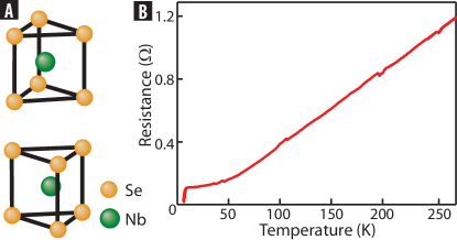
-NbSe2 is a layered transition metal dichalcogenide with a hexagonal structure and space group symmetry. The unit cell (Fig. S1A) consists of two sandwiches of Se-Nb-Se. The crystal typically cleaves between the neighboring Se layers, coupled by weak van der Waals forces.
Single crystals of -NbSe2 were grown by chemical vapor transport using iodine as the transport agent. A transport characterization of the sample batch used in this work is shown in Fig. S1B. The superconducting transition is observed at . The residual resistivity ratio (RRR), defined as the ratio of resistances , is .
SI II ’Ribbons’: Height and Orientation
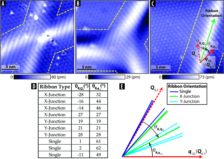
The CDW typically appears in regions which persist in one direction with apparent topographic elevation, forming a wide ’ribbon’ structure (Fig. S2A-C). We note that the topographic elevation as measured by maintaining a constant current with bias setpoint at lateral tip position can be given by
| (S1) |
Here is the true topographic corrugation of the sample, is a measure of the local tunnel barrier height (LBH), and is the local density of states (LDOS) of the sample at energy . Because of the logarithmic sensitivity of to the integral of the LDOS from the Fermi energy, (corresponding to ) up to the bias setpoint , STM topographs may contain electronic artifacts masquerading as geometric effects. Therefore, we present two pieces of evidence for the true geometric elevation of these ribbons.
First, a tabulation of the relative orientation of the ribbon to the nearest Bragg vector of the underlying hexagonal lattice for the various ribbons imaged in the study shows a seemingly random spread from to - the full range of available angles (Fig. S2D-E). Furthermore, these ribbon structures can intersect to form as well as junctions (Fig. S2A-B), and the angle between intersecting ribbons varies from to . The fact that ribbon orientation does not respect lattice symmetry strongly suggests a true geometric, rather than electronic origin of their apparent height. We contrast this observation with enhanced STM topographic corrugation associated with predominantly electronic features in a wide range of other materials, which respect the symmetry of the hexagonalHanaguri et al. (2010); Rutter et al. (2007) or squareWise et al. (2008) lattice.
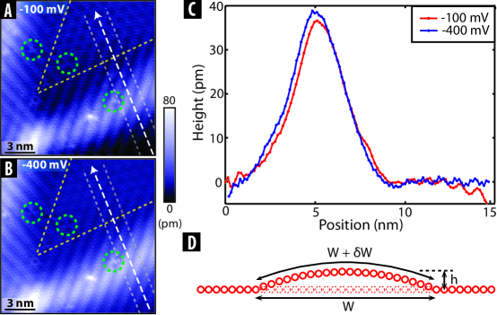
Second, the measured height of these ribbons in STM topographs exhibits dependence on bias setpoint within 400 mV below the Fermi energy (Fig. S3A-C). We note that this energy range over which the measured height of the ribbons is invariant is much larger than the spectral range of CDW variation in the DOS ( mV). We further note the contrast between the bias-independent ribbons, and single atom impurity resonances, whose measured ’height’ varies by between Fig. S3A and B. Therefore we conclude that the measured height ( pm) and width ( nm) of these ribbons has a predominantly geometric origin.
Having established the topographic origin of these ribbons (Fig. S2 and Fig. S3), we suggest that these ribbons are likely a topographic rippling of the top few layers. These ribbons may arise during the cleaving process due to underlying growth defects which can intercalate between Se-Nb-Se sandwich layers. We note that similar topographic ribbon deformations have recently been observed in another layered chalcogenide (Bi2Te3)Okada et al. (2012).
We estimate the in-plane and out-of-plane lattice strain associated with the topographic ribbon features. Using the maximum topographic elevation of an observed ribbon (40 pm), we can put an upper limit on the out-of-plane distortion by assuming that a minimum of 2 sandwich layers are elevated (any fewer, and the defects causing the elevation would be likely visible in our topographs). The out of plane distortion is therefore () of the unit cell spacing. To measure the in-plane distortion, we first use the Lawler-Fujita algorithmLawler et al. (2010), which can determine the lateral location of atoms with precision of the lattice spacingHamidian et al. (2012); Williams (2011). With this algorithm, we do not observe any change in the lattice constant across the ribbon, which places a direct experimental upper limit on the in-plane distortion of .
However, we can estimate the actual in-plane distortion indirectly from the measured out-of-plane distortion, by modeling the ribbon as a half-period of a sinusoid with height (40 pm) and width (10 nm) (Fig. S3D). The total lateral deformation due to such a ribbon is , corresponding to of the lattice spacing. As this is well below the resolution of the Lawler-Fujita algorithm, it is not surprising that the in-plane distortion is not detectable in STM topographs. From the upper bounds of on the vertical strain and on the lateral strain, we note that the magnitude of the strain field leading to the formation of these ribbons is moderate, in comparison to some other correlated materialsSlezak et al. (2008); Chu et al. (2010). We also note that while the magnitude of lattice distortion of these ribbons may seem small in the context of the observed quantum phase inhomogeneity, a comparison with other known materials suggests that strain of this magnitude can be sufficient to drive a transition to the unidirectional CDW phaseRu et al. (2008).
We previously discussed the ribbon orientation with respect to the lattice (); we now consider the ribbon orientation with respect to the CDW wavevector (), also detailed in Fig. S2D-E. In a simple picture of the strained ribbon structure, we would expect the ribbon-induced strain to couple strongly to the CDW orientation either parallel or perpendicular to the ribbon, and thus we would expect to observe values of either between or between . Yet we often find to be in the range as well. Insufficient statistics prevent us from inferring a clear connection between ribbon orientation and orientation, but the wide distribution of relative angles suggests the complexity of the interaction.
SI III Band Structure Calculations
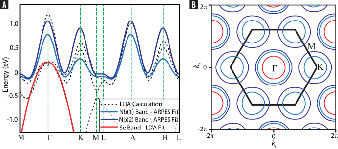
The band structure of -NbSe2 close to consists of two Nb- derived bands and one Se- ’pancake’-shaped hole pocketJohannes et al. (2006); Rossnagel et al. (2001). Close to , the Se- pancake-shaped hole pocket which surrounds the -point can be modeled by a simple quadratic form,
| (S2) |
With the values of and , this model accurately reproduces the dispersion obtained in LDA calculations by Johannes et al.Johannes et al. (2006), as shown in Fig. S4A. To model the Nb- bands, we use a tight-binding fit to the band structure observed in ARPES experiments, as reported by Rahn et al.Rahn et al. (2012). We find that a small () offset in the chemical potential relative to the parameters used by Rahn et al. was needed to reproduce the observed DOS from STM measurements. This offset is within the accuracy of the tight-binding fitting schemeRahn et al. (2012). The band energies of the tight-binding description are given byRahn et al. (2012)
| (S3) | ||||
where and and is along . The values of the tight binding parameters (including the offset) used in this work are:
| Parameter | Nb Band (1) | Nb Band (2) |
|---|---|---|
| 26.9 | 219.0 | |
| 86.8 | 46.0 | |
| 139.9 | 257.5 | |
| 29.6 | 4.4 | |
| 3.5 | -15.0 | |
| 3.3 | 6.0 |
SI IV Density of States Calculations
To calculate the DOS in the presence of a CDW, we impose a coupling between states connected by any one of the three -vectors, given by:
| (S4) |
The strength of the coupling is taken as a free parameter in the reproduction of the experimentally observed DOS, with a broadening parameter fixed at . Adjusting the size of slightly around the observed value of , we find the best match with STM spectra using (corresponding to the locally commensurate CDW periodicity), . With these parameter values, the gap structure in the calculated DOS closely approaches the overall shape, width and center of the gap structure seen in the measured data within of the Fermi energy , as shown in Fig. 5C.
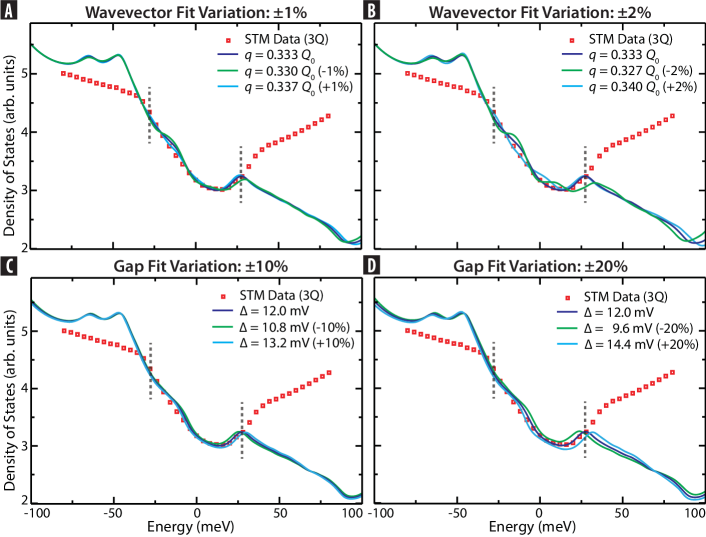
To demonstrate the accuracy of this fit, we show the effects of varying the wavevector by (Fig. S5A-B), and the gap value by (Fig. S5C-D). Using these fit parameter variations, we estimate the errors for and to be and respectively. The value of may however be an overestimate, leading to a systematic error of the same order as the fit uncertainty, since the described procedure does not take into account the particle-hole symmetric inelastic background in the experimental DOS. Accurate modeling of the inelastic background would require detailed temperature dependent spectroscopic data, which is beyond the scope of this work.
Crucially, we note that the particle-hole asymmetry in the CDW gap, with its minimum centered above , cannot be removed by the subtraction of a particle-hole symmetric background. Likewise, the striking deviation of our fitted gap parameter () from previous results (four times larger than the 3 meV value detailed by Borisenko et al.Borisenko et al. (2009), and three times smaller than the 35 meV value detailed by Hess et al.Hess et al. (1991)) far exceeds fit or systematic uncertainties.
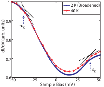
To experimentally verify the lack of bearing of the kinks on the CDW phase, we performed spectroscopy up to , and universally observed the presence of these kinks in the STM spectra well above (). A comparison of the typical spectrum acquired at to that acquired at , is shown in Fig. S6. We note that the data acquired at are thermally smeared by , i.e. , resulting in a broadening of the kinks. Despite this, the kinks remain distinguishable, and are present throughout all spatial regions studied in this work.
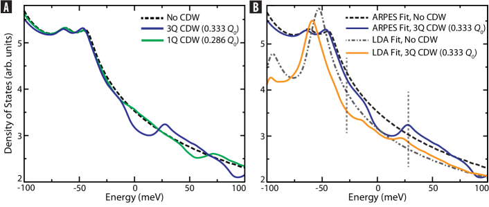
For completeness, we show in Fig. S7A the calculated DOS in the presence of a CDW at the experimentally observed wave vector, , using . The lack of correspondence between this calculation (green curve in Fig. S7A) and the measured spectrum (green curve in Fig. 5B) can be attributed to the increased intensity of the inelastic background in the buckled region of the ribbons. This background is evident in the -shape of the spectrum in Fig. 5B, centered close to , as explained theoreticallyKirtley et al. (1992) and observed experimentally across a wide variety of materialsKirtley et al. (1992); Kirtley and Scalapino (1990); Niestemski et al. (2007); Fridman et al. (2011); Arai et al. (2001); Rahnejat et al. (2011); Collins et al. (1984); McMillan and Mochel (1981).
We also compare our results to a calculation of the DOS based on a tight-binding fit to the full three-dimensional LDA band structure reported by Johannes et al.Johannes et al. (2006). The DOS obtained using this 3D LDA fit is compared to the results based on the 2D fit in Fig. S7B. We find that the STM data are best reproduced using the band structure observed by ARPES, and that there is a noticeable difference between the depths of the gaps in the two-dimensional ARPES based and three-dimensional LDA-based band structure fits (despite independent parameter optimization), which is indicative of some difference between the surface and bulk dispersionsJohannes et al. (2006).