Thermoelectric and thermomagnetic effects Transition-metal compounds Ab initio calculations
Doping effect on thermoelectric properties of MoS2
Abstract
We systematically study thermoelectric properties of layered MoS2 by doping, based on Boltzmann transport theory and first-principles calculations. We obtain optimal doping region (around 1019 cm-3) by looking closely to the temperature and doping level dependent thermopower, electrical conductivity, power factor (PF) and ultimately figure of merit (ZT) coefficient along in-plane and cross-plane directions. MoS2 has a vanishingly small anisotropy of thermopower but a big anisotropy of electrical conductivity and electronic thermal conductivity in optimal doping region. is comparable to in the plane while dominates over across the plane. ZT can reach as high as 0.3 at around 700 K. In-plane direction is demonstrated to be more preferable for thermoelectric applications of MoS2 by doping.
pacs:
72.20.Papacs:
72.80.Gapacs:
31.15.A-1 Introduction
Thermoelectrics play a key role for power generation and refrigeration [1, 2, 3]. Chalcogenide composite materials, such as Bi2Te3, PbTe and others [4, 5, 6, 7, 8, 9, 10], have attracted much research interest for decades because of their high performance on thermoelectric conversion. Transition-metal dichalcogenide MoS2, one prototype material in chalcogenide family, has distinctive electronic, mechanical, catalytic and tribological properties [11, 12, 13, 14, 15, 16, 17, 18, 19, 20]. Recent research on its optical properties [21] and lattice dynamics [22, 23] has aroused renewed interest but its thermoelectric properties have barely been studied [24]. Nevertheless, the lowest thermal conductivity obtained experimentally in a MoS2-related structure [25], together with an unusually large thermopower [26, 28, 27] found in MoS2, may render it a promising candidate for thermoelectric application.
Unfortunately, available experimental data concerning the thermoelectric transport properties of MoS2 are quite scarce and fragmentary in literature. The most significant experimental work was performed by Mansfield and Salam [27] and Thakurta et. al. [26], who studied temperature dependence of the electrical transport properties including thermopower and electrical conductivity at only three samples with low dopings, but failed to investigate on the thermal-related properties. Kim et. al. [29] merely worked on the thermal conductivity . Based on these incomplete experimental data, it is difficult to estimate the figure of merit ZT coefficient which is crucial to evaluate thermoelectric conversion capability. Moreover, available extrinsic carrier concentrations in MoS2 single crystals were quite low. It remains a big challenge to obtain a wide doping region in experiment but nonetheless is essential to tuning carrier density appropriate for an optimum ZT.
In this letter, we study theoretically the thermoelectric transport properties of MoS2 over a range of doping level (from 1015 to 1020 cm-3) for an optimization of its thermoelectric conversion efficiency. We have the following findings: (1) Thermopower is attainable more than 200 V/K over a wide range of dopings and directional anisotropy vanishes between in-plane and cross-plane thermopowers for doping level above 1017 cm-3. (2) Anisotropic electronic scattering time exists between in-plane and cross-plane directions, which accounts for two orders of magnitude difference between electrical conductivities and and also gives rise to anisotropy between electronic thermal conductivity and . (3) In optimal doping region, is comparable to in the plane while dominates over across the plane. (4) Carrier density around 1019 cm-3 is sufficient for optimal thermoelectric performance, figure of merit ZT coefficient reaches 0.3 at 700K within the plane. (5) A preference for in-plane over cross-plane direction by doping for thermoelectric applications of MoS2 is demonstrated.
2 METHODOLOGY
The band structure of MoS2 is calculated by using the general potential linearized augmented plane-wave(LAPW) method as implemented in the WIEN2K package [30]. The electronic exchange-correlation is described within the generalized gradient approximation (GGA) of Perdew-Burke-Ernzerhof(PBE) flavor [31]. We use 5000 k points in the full Brillouin zone(BZ) to achieve a total energy convergence better than 1 meV/atom. MoS2 has P63/mmc space group symmetry and consists of a hexagonal plane of molybdenum atoms sandwiched by two hexagonal planes of sulfur atoms. The unit cell contains two alternating and weakly van-der-Waals-bonded layers with an AB stacking along c axis. The experimental lattice parameters [32] (a = 3.16, c = 12.295) are used here.
We calculate transport properties based on Boltzmann transport theory applied to the band structure. In the following part, we discuss the dependence of transport functions including thermopower S, electrical conductivity , power factor(PF), and ultimately figure of merit coefficient ZT on temperature and doping level along two perpendicular directions. The electron scattering time is assumed to be independent of energy due to its good description of S(T) in a number of thermoelectric materials [6, 33, 34]. In this sense, no adjustable parameters are needed to calculate those transport functions. The integration is done within the BOLTZTRAP transport code [35]. A very dense mesh with up to 18000 k points in the BZ is used.
3 RESULTS AND DISCUSSION
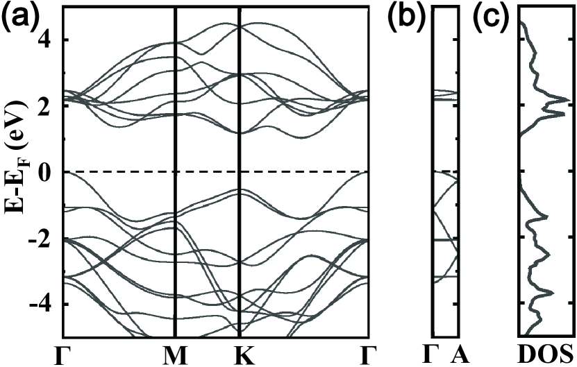
An improved band gap is essential for calculating transport properties, so the Engel-Vosko GGA (EV-GGA) formalism [36] is applied to calculate the band gap more accurately. In Fig. 1, we present our calculated band structure and density of states of MoS2. The in-plane and cross-plane cases are considered separately in Fig. 1(a, b). In Fig. 1(a), an indirect gap of 1.04 eV is obtained between top of valence band at and bottom of conduction band at one k point from K to . A similar band structure calculated from standard PBE-GGA formalism gives an indirect gap of 0.84 eV, which agrees with reported value [37]. Compared with 1.20 eV from experiment [38], it is clear that EV-GGA does improve the band gap calculation upon PBE-GGA. In contrast to the pronounced dispersive in-plane electronic bands shown in Fig. 1(a), the cross-plane bands shown in Fig. 1(b) are quite flat, showing a very weak cross-plane bonding due to Van der Waals interaction. The structural anisotropy induces an anisotropy between in-plane and cross-plane band gaps. The calculated cross-plane gap is found to be 2.20 eV.
Besides the band gap anisotropy, a strong asymmetric feature of band structure between valence and conduction bands implies that the thermoelectric properties of n-type MoS2 would be very different from that of p-type. The heavy and doubly degenerate bands near the conduction-band minimum suggest that the n-type MoS2 would have better thermoelectric performance. In Fig. 1(c), total density of states (DOS) also shows this preference, there is a comparatively higher DOS very close to the conduction band edge than that near the valence band edge. Considering more experimental data are found for p-type in literature [28, 27, 26], we focus on hole-doped MoS2 in this study.
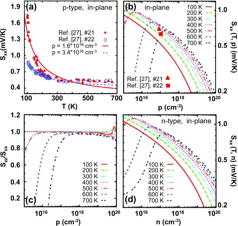
In-plane and cross-plane thermopower are firstly studied. We initially compare our calculated S with experimental data from Mansfield and Salam [27] in Fig. 2(a,b). Samples in their experiment were p-type from nature with hole carrier concentration as low as 1015 1017 cm-3. A very good agreement is obtained. Both our calculation and available experimental data show a value of in-plane thermopower S higher than 400 V/K and S decreases with increasing temperature as shown in Fig. 2(a). Then we extend our discussion to high doping of 1017 1020 cm-3 (corresponding to p = 10-5 10-2 holes per unit cell in our case) where thermoelectric properties are expected to be optimized as predicted from theory [39] and experimentally observed in many materials [40, 41, 42]. It also applies in MoS2 as we will show later. From Fig. 2(b), the thermopower in the high doping region, though decreasing with doping level, takes a value of at least 200 V/K (ZT2.4 is expected from the Wiedemann-Franz law.) and increases with increasing temperature. To see a possible anisotropy between in-plane and cross-plane S, we then show the ratio of Szz over Sxx in Fig. 2(c). A relatively high anisotropy of thermopower below 1017 cm-3, possibly due to difference of effective mass (or mobility) and density between band-edge carriers moving along two directions, according to the Mott formula[43] S where n, are respectively carrier density and mobility. Anisotropy vanishes as doping goes above 1017 cm-3 and both Sxx and Szz show similar magnitude and dependence on hole doping level and temperature, which is different from layered conductive thermoelectric oxides [44, 45]. Finally, to confirm that n-type MoS2 may be better, we briefly compare n-type in Fig. 2(d) with p-type in Fig. 2(b). Expectedly, bigger value of thermopower of n-type MoS2 than of p-type is found.
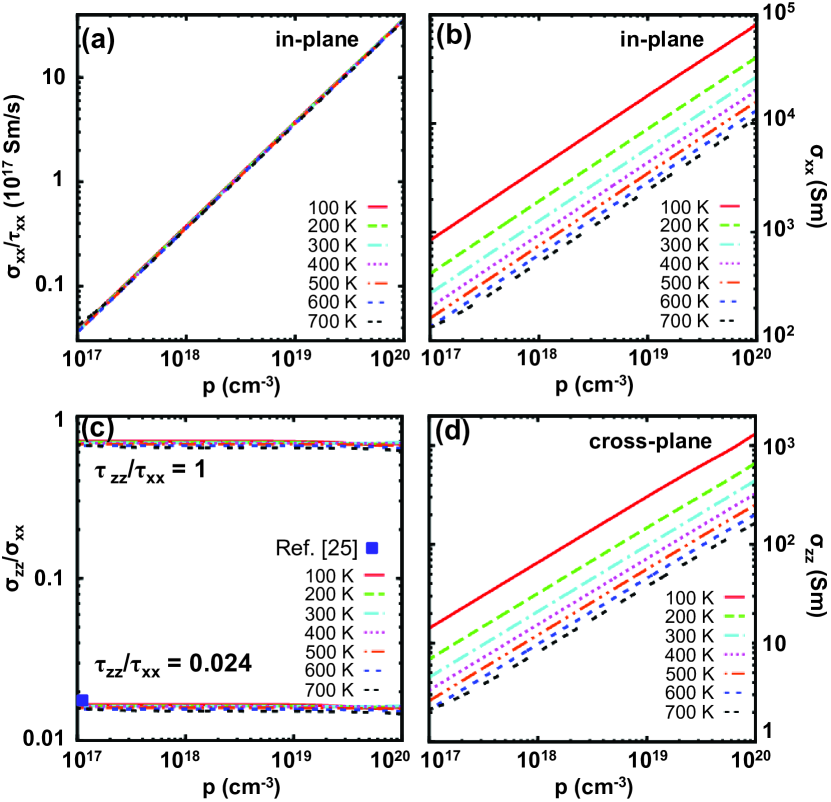
Based on the energy-independent scattering time approximation, it is quite straightforward to get doping dependence of / at various temperature from the electronic band structure, upon which we calculate if is known. In Fig. 3(a), we show calculated / depending on hole doping and temperature. We find an almost temperature independence but an approximately linear doping level dependence of /, namely / T0 p. For a quadratic band dispersion in an electron-phonon approximation, p T-1 stands, this results in T-1p, in consistent with the analytical treatment of carriers scattered by lattice vibrations in a semiconductor [43, 6]. To calculate , we need some experimental input to get . Here we use = 0.16 at 100 K and 1.41015 cm-3 doping level from the experimental data by Thakurta et. al. [26] and get = 3.04 10-6 T-1p with Kelvin and cm-3 as the unit of T and p, respectively. Plugging it into our calculated /, we show in Fig. 3(b), and power factor in Fig. 4(a).
Electrical conductivity along c axis is also calculated and a strong anisotropy is found between the in-plane and cross-plane carrier scattering time . When isotropic is assumed, namely, = 1, we obtain / close to unity in Fig. 3(c), which is against the reported result [26]. To fit / of two orders of magnitude in experiment, we use anisotropic = 0.024, which suggests that a strong anisotropy of carrier scattering time should play a role in this system, and therefore obtain = 7.30 10-8 T-1p. Finally, we are able to calculate and show it in Fig. 3(d).
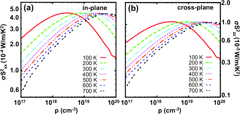
With thermopower and electrical conductivity available, we are able to evaluate power factor. For an optimized thermoelectric performance, peak value of PF, the corresponding doping level and temperature are more concerned here. Both power factors along two perpendicular directions have peak values spanning in a wide doping range from 1017 to 1020 cm-3. From Fig. 4, the value of peak power factor is nearly constant, while its temperature increases with the hole doping level. Due to the anisotropic carrier scattering time , nearly 50-fold difference is found between in-plane and cross-plane power factors, e.g., and maxima at 700 K are respectively 4.110-4 W/m/K2 and 1.010-5 W/m/K2. The in-plane PF value is close to that of good thermoelectric materials [39].
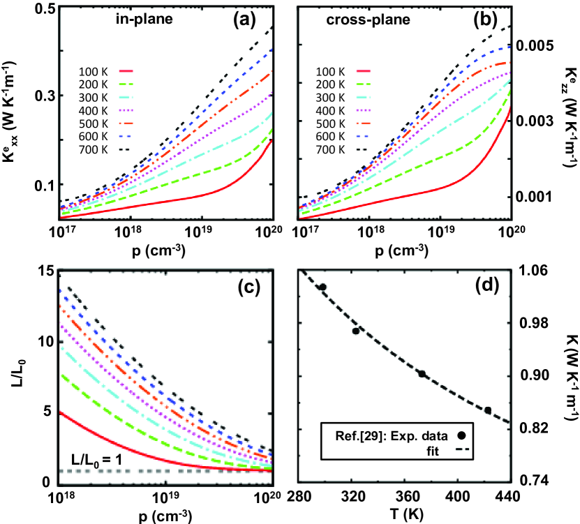
To optimize ZT value, it is also essential to know thermal conductivity , including electronic and lattice . Based on the scattering time approximation previously discussed, we firstly calculate electronic thermal conductivity and show it in Fig. 5(a,b). increases with carrier density p and temperature. At least two orders of magnitude difference between and are found, which is consistent with electrical conductivity case. Usually one gets from electrical conductivity by using the Wiedemann-Franz law, namely /( T) = 2.4410-8 WK-2, the so-called Lorenz number. However, it seems not the case here. In Fig.5(c) we normalize L(=/( T)) by the Lorenz number and plot it as function of doping and temperature. L/L0 is close to one as carrier density goes beyond 1020 cm-3. Unlike the electronic , the lattice can’t be calculated from electronic band structure. Here we simply use experimental data from literature [29] and show it in Fig. 5(d). Kim et. al. [29] measured temperature dependence of for MoS2 sample as shown by filled circles in Fig.5(d). The lattice thermal conductivity dominates in the cross-plane direction, with two orders of magnitude bigger than . While the in-plane is comparable to . We fit the experimental data by using = 183.103/T + 0.412671. It seems that Umklapp process which usually has 1/T shows up and thermal conductivity gets softening with increasing temperature.
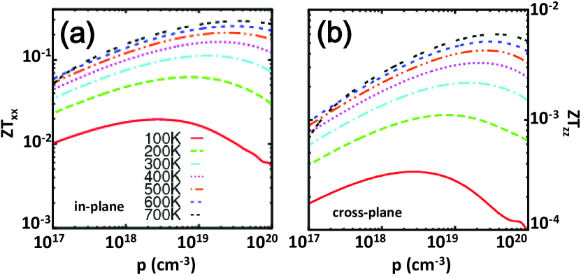
All the data obtained above allow us to calculate ZT as function of temperature and hole doping along two directions, which is shown in Fig. 6(a-d). Optimum ZT value increases with increasing temperature, so does the corresponding optimum doping level. In-plane is better than cross-plane for thermoelectric conversion, with its ZT up to 0.30 and saturated around 700 K, as shown in Fig.6(a,b). We may further reduce by random stacking according to Kim [29] and Chiritescu et. al. [25], but its effect on electrical transport needs to be checked if it may compromise the gain of ZT by reducing thermal conductivity.
4 CONCLUSION
By combining ab. initio. band structure calculation with semi-classical Boltzmann transport theory, we theoretically studied the doping and temperature dependence of thermoelectric transport properties of 2H-MoS2. Anisotropic electronic scattering time has to be considered to account for difference between in-plane and cross-plane electrical conductivity , which also gives rise to anisotropy of electronic thermal conductivity . In-plane is comparable to lattice while cross-plane lattice dominates over lattice . In contrast to the anisotropy of and , thermopower, which is attainable more than 200 V/K over a wider range of doping and temperature, shows a vanishing anisotropy for doping over 1017 cm-3. The maximum ZT can reach as high as 0.3 at around 700 K with carrier density of 1020 cm-3, and may go higher if restacking process is used to further reduce the thermal conductivity. A preference for the in-plane thermoelectric transport by doping is demonstrated.
Acknowledgements.
This work was supported by the NSFC under Grant No. 11004201, 50831006 and the National Basic Research Program (No. 2012CB933103). T.Y. acknowledges the IMR SYNL-Young Merit Scholars and T.S. K research grant for support.References
- [1] Brian C. Sales, Science 295, 1248 (2002).
- [2] A. Majumdar, Science 303, 777(2004).
- [3] H. Bttner et. al., MRS Bull. 31, 211 (2006).
- [4] T. Tritt (Vol. Editor), Recent Trends in Thermoelectric Materials Research vol. 69-71 (Semiconductors Semimetals) Academic Press, San Diego (2001).
- [5] J. Androulakis et. al., Phys. Rev. B 83, 195209 (2011).
- [6] K.P. Ong, D.J. Singh and P. Wu, Phys. Rev. B 83, 115110 (2011).
- [7] D. Parker and D.J. Singh, Phys. Rev. B 82, 035204 (2010).
- [8] H. Goldsmid, A. Sheard, D. Wright, Br. J. Appl. Phys. 9, 365 (1958).
- [9] R. Venkatasubramanian, E. Siivola, T. Colpitts, Nature 413, 597 (2001).
- [10] N. F. Hinsche, B. Yu. Yavorsky, I.mertig, P. Zahn, Phys. Rev. B 84, 165214 (2011).
- [11] L. Rapoport et. al., Nature(London) 387, 791 (1997).
- [12] J.M. Martin et. al., Phys. Rev. B 48, 10583–10586 (1993).
- [13] B.C. Gates, Catalytic Chemistry, Wiley, New York (1992).
- [14] X. Zong et. al., J. Am. Chem. Soc. 130, 7176 (2008).
- [15] I.T. McGovern et. al., Surf. Sci. 152/153, 1203 (1985).
- [16] B. Radisavljevic et. al., Nature Nanotechnology 6, 147 (2011).
- [17] Y.B. Li, Y. Bando, and D. Golberg, Appl. Phys. Lett. 82, 1962 (2003).
- [18] E. Gourmelon et. al., Sol. Energy Mater. Sol. Cells 46, 115 (1997).
- [19] J. Chen et. al., J. Am. Chem. Soc. 123, 11813 (2001).
- [20] J. Xiao et. al., Chem. Mater. 22, 4522-4524 (2010).
- [21] K.F. Mak, C. Lee, J. Hone, J. Shan, and T.F. Heinz, Phys. Rev. Lett. 105, 136805 (2010).
- [22] C. Lee et. al., ACS Nano 4, 2695 (2011).
- [23] C. Ataca, M. Topsakal, E. Aktrk, and S. Ciraci, J. Phys. Chem. C 115, 16354-16361 (2011).
- [24] H.H. Guo, T. Yang, P. Tao, Y. Wang, Z.D. Zhang, J. Appl. Phys. 113, 013709 (2013).
- [25] C. Chiritescu et. al., Science 315, 351 (2007).
- [26] S.R. Guha Thakurta and A.K. Dutta, J. Phys. Chem. Solids 44, 407 (1983).
- [27] R. Mansfield and S.A. Salam, Proc. Phys. Soc. B 66, 377 (1953).
- [28] M.K. Agarwal and L.T. Talele, Sol. State Comm. 59, 549 (1986).
- [29] J.-Y. Kim et. al., Bull. Korean Chem. Soc. 31,3225 (2010).
- [30] P. Blaha et. al., WIEN2k: An augmented plane wave plus local orbitals program for calculating crystal properties (TU Vienna, Vienna, 2011).
- [31] J.P. Perdew, K. Burke and M. Ernzerhof, Phys. Rev. Lett. 77, 3865 (1996).
- [32] R. Coehoorn et. al., Phys. Rev. B 35, 6195 (1987).
- [33] D. Parker, M.-H. Du, and D.J. Singh, Phys. Rev. B 83, 245111 (2011).
- [34] L. Zhang and D.J. Singh, Phys. Rev. B 80, 075117 (2009).
- [35] G.K.H. Madsen, K. Schwarz, P. Blaha, and D.J. Singh, Phys. Rev. B. 68, 125212 (2003).
- [36] E. Engel and S.H. Vosko, Phys. Rev. B 47, 13164 (1993).
- [37] S.W. Han et. al., Phys. Rev. B, 84, 045409 (2011).
- [38] K.K. Kam and B.A. Parkinson, J. Phys. Chem. 86, 463 (1982).
- [39] G.D. Mahan, ”Good Thermoelectrics” in Solid State Physics vol. 51, ed. by H. Ehrenreich and F. Saepen (Academic Press, San Diego, 1998).
- [40] D.M. Rowe and G. Min, J. Mater. Sci. Lett. 14, 617-619 (1995).
- [41] Y. Zhang et al., Phys. Rev. Lett. 106, 206601 (2011).
- [42] G.J. Snyder and E.S. Toberer, Nature Materials 7, 105 (2008).
- [43] J. M. Ziman, Principles of the theory of solids, 2nd Ed.(Cambridge University Press, 1995)
- [44] K.P. Ong, D.J. Singh and P. Wu, Phys. Rev. Lett. 104, 176601 (2010), K.P. Ong, J. Zhang, J.S. Tse and P. Wu, Phys. Rev. B 81, 115120 (2010).
- [45] G.D. Tang, H.H. Guo, T. Yang and et. al., Appl. Phys. Lett. 98, 202109 (2011).