This work was supported in part by the Defense Microelectronics Activity under the Advanced Technology Support Program.
An 8-bit carry look-ahead adder with 150 ps latency and
sub-microwatt power dissipation at 10 GHz
Abstract
Reciprocal Quantum Logic combines the speed and power-efficiency of single-flux quantum superconductor devices with design features that are similar to CMOS. We have demonstrated an 8-bit carry look-ahead adder in the technology using combinational gates with fanout of four and non-local interconnect. Measured power dissipation of the fully active circuit is only 510 nW at 6.2 GHz. Latency is only 150 ps at a clock rate of 10 GHz.
I Introduction
Superconducting Reciprocal Quantum Logic (RQL) is an ultra-low-power technology for high-performance computing that gives unmatched efficiency in terms of operations per joule RQL11 . Simple experiments have shown bit energy approaching 1000 , with further reduction expected using smaller devices. This means that the technology offers two orders of magnitude power savings over 22 nm CMOS even after taking into account the overhead of the cryocooler, of order 1000 W/W at an operating temperature of 4.2 K Coolers . RQL introduces a combination of new features that are unattainable by other superconducting logic families Likharev_91 , e-RSFQ , including zero static power dissipation, stable timing, low bit-error-rate, low active-device count, and low-latency. The logic is combinational with multiple levels of logic per pipeline stage, following conventional CMOS behavior. This allows a wealth of CMOS design tools and methods to be applied. A small-current AC waveform provides power and a stable clock reference to each gate, which in principle allows the technology to scale to VLSI.
Here we report the design, fabrication, and test of an RQL 8-bit carry look-ahead (CLA) adder as a benchmark to demonstrate the effectiveness of the logic in a larger circuit. The CLA adder is an important hardware component for low-latency parallel addition. However, implementation of this circuit has been a major challenge for superconducting technology in the past. Gate-level pipelining and inefficient clock distribution resulted in designs with high latency that defeated the purpose bunyk_99 . Asynchronous or self-timed designs can reduce latency kameda1999self ; Filippov11 , but high active device count, high current bias, and timing uncertainty limit increased integration scale. The RQL implementation of the adder achieves a tenfold improvement in latency and Josephson-junction device count over earlier designs and shows that the main metric, power efficiency, is scalable to a large circuit as predicted by the first simple tests.
II Logical Design
The adder, shown schematically in Fig. 1, computes the carry bits with minimal latency at the expense of four-way fan-out and high-density, long interconnects. The design is a Kogge-Stone radix-2 implementation that for N-bit inputs consists of stages. The first stage (A/OR) produces carry propagate and carry generate signals. The following stages form the carry look-ahead (CLA) network that computes all carries in parallel. The final result is computed in the last stage where carries are summed with the input sums using logical XOR.

The A/OR stage produces logical AND and OR for input bits and , expressed as , and . These outputs are the generate and propagate signals, which have fanout of up to four to reach multiple CLA blocks in the second stage. Each stage of the CLA network takes select inputs from the previous stage and , and computes expressed as , and . For the stage, input selection obeys . Inputs and outputs of the CLA blocks are pruned to stay within boundaries and to produce only the culminating generate bits, which correspond to carries . The final sum is computed as .
RQL allows efficient design of the adder in terms of device count and latency. Unlike other superconductor logic, RQL gates are combinational with behavioral descriptions similar to CMOS. As in CMOS circuits, this allows use of multiple levels of logic per pipe-line stage that greatly reduces latency. RQL logic has an additional efficiency in wave pipelining that eliminates active latches to synchronize signals at each stage. Instead, four-phase power is used to move signals from stage to stage on the rising edge of the power waveform, which also serves as the clock. Data propagation speed finds equilibrium independently of initial conditions, clock amplitude, parameter variations, and data pattern. For the 8-bit adder, 8 parallel clock lines provide power to each bit. There is no skew between clock lines provided that their geometrical lengths are equal. Each of the five stages of the adder takes one phase of the clock, which amounts to a total of 1.25 clock cycles for the computation to complete.
RQL gates have no static power dissipation. Power is only dissipated for logical “ones”, physically encoded as a pair of positive and negative (reciprocal) single-flux-quantum (SFQ) pulses. The dynamic power dissipation is , where is the average critical current of the Josephson junctions, is the number of junctions, mV ps is the flux quantum, is operating frequency, and the prefactor of 0.33 is experimentally determined RQL11 . AC loss in the superconducting line is small loss . The AC power is applied through weak inductive coupling, which leads to important advantages: the gates are powered in series requiring small current, and dynamics in the circuit do not affect timing. An RQL circuit scaled to 2 million Josephson devices of 0.1 mA average critical current would dissipate only 1.4 mW of power when fully active. Applied power would need to be larger than dissipated power in order to maintain clock stability in terms of amplitude and timing. Since operating margins of the gates are sufficient to tolerate % variation in clock current, only 4 mW of clock power would be needed to power the 2-million-device chip, amounting to only 9 mA of current on a 50 line. Timing variation would amount to only 5 ps, or % of the clock period at 10 GHz RQL11 .
The adder was designed using gate-level VHDL models. Only two basic RQL logic gates were used: AndOr and AnotB RQL11 . The AndOr gate propagates the first logical “one” input in a given clock cycle to the Or output, and the second “one” input to the And output. The AnotB gate propagates a logical “one” on the A input to the output unless a logical “one” on the B input comes in the same clock cycle. Logical XOR can be expressed as “A or B, but not both A and B,” which is implemented by connecting the outputs of the AndOr gate to the inputs of AnotB gate. The CLA block, shown in Fig. 1, contains And and Or gates. These are implemented by pruning the outputs of the AndOr gate. RQL gates require active interconnect, consisting of two sequential Josephson junctions, for signal amplification. The same active interconnect is used both in splitters to produce fanout, and to produce a delay element. The five less-significant carries use delay cells to reach the last column. The AnotB gates in the second column produce the partial sum are in parallel with the CLA network and also use delay cells. The three more-significant carries set the overall latency of the circuit, and achieve up to eight levels of logic for a pipeline stage consisting of all four clock phases.
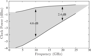
The adder design was verified using WRSpice, a physical-level circuit simulator that includes a device model for the Josephson junction wrspice . Simulated operating margins on clock power as a function of frequency for the entire eight-bit adder are shown in Fig. 2. The upper limit corresponds to over-bias and is relatively frequency independent. The lower limit narrows the operating region with frequency, indicating that the circuit is latency-limited at high clock rate. The Josephson junction model used was for 1.5 m devices with a critical current density of 4.5 kA/cm2 and an product of 0.7 mV, where is the critical current, typically 141-200 A in our circuit, and is the external shunt resistance. Such devices produce voltage pulses equal to the single-flux quantum, about 0.7 mV high and 3 ps wide. Device delay for sequentially wired junctions is also about 3 ps under nominal clock power. A clock rate of 10 GHz was the design target as there are up to eight sequential junctions per phase and four phases per clock cycle. In the circuit simulation, this clock rate gives a wide clock-power operating margin of 4.6 dB.
III Physical design
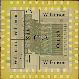
The CLA 5 mm 5 mm chip is shown in Fig. 3. The circuit includes four passive, microwave Wilkinson power splitters for clock distribution Oberg11WPS and eight distributed amplifiers Herr2010high to output the result to room temperature. A 16-stage shift register with a single serial input is used to generate the two input words. Taps on the shift register feed the CLA inputs: starting with the LSB of input word A and working up, then wrapping around to the MSB of word B and working back down. In this way an arbitrary combination of input words can be applied every 16 clock cycles, with the same bits reused in different combinations in the intermediate clock cycles.
The circuit was designed for a Nb superconductor foundry service Hypres that is more than adequate to yield the circuit. However, process integration scale is quite modest by CMOS standards, with only four metal layers and 4 m wire pitch, which limits circuit density. Two metal layers were used either for double ground planes surrounding the logic gates or for clock stripline, leaving only the remaining two metal layers for gates and interconnect.
To accommodate physical layout, an additional idle phase consisting only of delay cells was added before the last CLA column to allow the three longest active interconnects to cover distance. This increased the total number of clock phases to six, which amounts to 1.5 clock cycles or 150 ps latency at a 10 GHz clock rate. In the final design the three long active interconnects were replaced by 5 passive superconducting striplines, which propagate signals at a 100 m/ps speed-of-light. The signals are received by active interconnect circuits with the timing constraint that the receiver must be near the peak of the clock waveform to receive the positive pulse.
The clock distribution network is implemented as two eight-way Wilkinson power splitters for the in-phase and quadrature clock phases, and two identical Wilkinson devices used in reverse to recombine the eight lines onto a single line Oberg11WPS . In this way the AC clock enters and exits the chip without ever contacting chip ground. The 32 impedance of the clock lines on chip is the largest impedance achievable using the bottom metal layer, with a 2 m minimum line width, and using the top metal layer as ground. The Wilkinson splitters were designed for a center frequency of 7.5 GHz, and optimized to give better than 30 dB return loss from 5-10 GHz, and isolation better than 15 dB over the same range. A second version of the design used splitters centered at 15 GHz. A six-section design was chosen to transform the 50 impedance of the feed line to the effective 4 impedance of the eight 32 clock lines in parallel. The circuit design requires a nominal clock amplitude of 2 mA per line. Total input on each of the two clock lines amounts to only 3.2 mA rms.
IV Circuit Test

Each chip is mounted in a pressure-contact cryoprobe and cooled to 4.2 K in a liquid helium dewar. The input is supplied from a digital pattern generator through an inductive coupling to produce SFQ signals on-chip, and returns to room temperature to be observed. The pattern generator is phase-locked to a synthesizer that generates the clock sinusoid, followed by a 90-degree hybrid to split the clock into in-phase and quadrature. The clock lines also return to room temperature after inductive couplings on chip and were terminated in 50 loads. The eight output bits from the adder are converted from SFQ signals to source-terminated voltages of 2 mV peak-to-peak on-chip.
The high-speed input and output waveforms indicating correct digital operation of the circuit are shown in Fig. 4. The input waveform is non-return-to-zero, while the output waveforms are return-to-zero and are inverted by low-noise amplifiers at room temperature. The visible feed through of the clock sinusoids to the outputs is frequency dependent and is attributed to pickup in the cryoprobe package. Feed through from the 2 dBm clock lines to the outputs is down by 45 dB, which is small in absolute terms but is comparable to the 47 dBm output levels. This effect could be eliminated in a future chip design by using differential output.
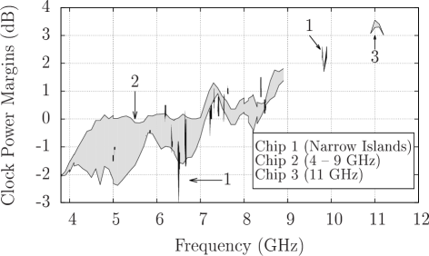
In simulation, the frequency-dependent operating margins on clock power were limited by signal propagation time in the digital gates. In test, power margins can be dominated by the microwave design of the circuit, including the cryoprobe package. Different versions of the chip were tested in two different cryoprobes, as shown in Fig. 5. The narrowband probe had a two-layer printed circuit board (PCB) for signal traces and ground. Chip test using this probe showed very strong frequency dependence and was functional only in narrow frequency bands in the range 5-10 GHz. The highest observed frequency for correct operation was 9.8 GHz. The wideband cryoprobe had a redesigned PCB and used a second ground plane to minimize crosstalk from the clock lines. The probe transition from coaxial line to stripline on-chip was optimized to give a return loss of better than 20 dB from dc up to 20 GHz. Chip test using the wideband probe produced a single large, continuous operating region that extended from 4-9 GHz. Another test, using the wideband probe and a chip with the Wilkinson power network scaled up by a factor of two in frequency, produced a small operating region observed around 11 GHz.
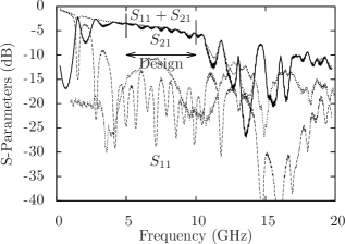
Digital operation of the chip (Chip 2 in Fig. 5) can be compared to S-parameter measurements of the clock distribution network of the same chip, shown in Fig. 6. The sum of transmitted and reflected power measured on the clock line roughly corresponds to the round-trip attenuation of the cables in the probe, indicating small losses due to radiation and coupling to other lines across the entire frequency range up to 20 GHz. Transmitted power shows the bandwidth of the Wilkinson splitter to be about 4-10 GHz, and the center appears to be consistent with the 7.5 GHz design value. Small reflected power is a key figure of merit, as resonances create standing waves, leading to non-uniform biasing of the circuitry and narrowed clock power operating margins. Within the bandwidth of the Wilkinson, reflected power is 10-22 dB less than transmitted power, with several resonances visible. Qualitatively similar behavior was observed for the low bandwidth probe. However, there appears to be little correlation between power margin measurements of the digital circuit and these resonances. This indicates that S-parameter measurements alone cannot adequately predict frequency-dependent digital operation of the chip. In any case, for any specific application the clock will be single-tone and thus narrow-band. This significantly relaxes microwave design constraints.
V Power Dissipation Measurement
A final test measured dynamic power dissipation of the circuit. This is done by observing the attenuation of the clock signals due to the power draw of device-switching events in the circuit. With an applied clock power of about 0.6 mW, the measurement must be sensitive to better than one part per thousand to be able to resolve the expected dissipation.
To achieve this accuracy we use a modulation technique where the input data pattern is periodically chopped, alternating between all-zeros and a pseudo-random pattern. Since none of the Josephson junction devices in the circuit are active for an all-zeros input, this modulates the AC clock signal at the data chopping frequency, producing sidebands that are measurable with a spectrum analyzer. Dynamic power dissipation of the circuit is calculated from the power in the sidebands.
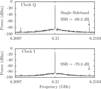
Fig. 7 shows the spectra of the two clock lines returned from the chip. The two clock quadratures I and Q had respective power levels of 2.4 dBm and 2.0 dBm at the chip, measured as the geometric mean of applied and returned power to account for attenuation in the probe cables. Sidebands are visible above and below the carrier with a spacing of 259 kHz, which corresponds to the fundamental of the modulating square wave. The power ratio between a single sideband and the carrier, , was measured to be 69.3 dB for clock Q and 79.3 dB for clock I. Additional sidebands corresponding to higher odd harmonics of the square wave fall outside the frequency range of our measurement.
The sidebands can arise either by amplitude modulation (AM), or by phase modulation (PM). Both may be present in the the CLA adder circuit, but only AM is indicative of power dissipation. The Josephson junction circuit elements, which are inductively coupled to the clock, are effectively in series with the clock line. The non-switching junction can be modeled as an inductor, the switching junction as a resistor. The switching junctions take power from the clock line, producing AM, and decrease the propagation speed of the clock, which gives rise to PM. We will first establish an upper bound on power dissipation assuming purely AM, and then estimate dissipation accounting for the relative contributions of AM and PM, using previously reported measurements of an RQL circuit RQL11 .
For the case of purely AM, the ratio of power dissipated to power in the clock line, , where and are the maximum and minimum amplitude of the clock sinusoid. is the amplitude of the clock carrier and is the amplitude of the square wave modulation. The factors of two account for the presence of double sidebands, one above and one below the carrier frequency. The fundamental of the square wave has an amplitude relative to the amplitude of the square wave itself, so the amplitude of the single sideband, . The normalized power dissipation is
| (1) |
This is an upper bound on power dissipation on the chip. It would also be possible to produce the power spectrum measured in Fig. 7 by phase modulation, without any power dissipation. Our previous measurement of clock stablilty in an RQL shift register provides an estimate of the relative contributions of AM and PM to the power spectrum.
In order to estimate the AM and PM contributions to measured sideband power we calculate the factors and corresponding to the AM and PM amplitudes for a simple sine-modulated waveform
| (2) |
where and are the amplitude and frequency of the carrier, and is the frequency of the modulation. From this equation can be found by solving , as the waveform amplitude ranges over . Similarly, can be found by solving , as the waveform phase ranges over . Both the data-modulated power ratio, , and a data-modulated time delay, ps, were previously reported in RQL11 for an RQL shift register operating at 6 GHz. These measurements give and , indicating that AM and PM are about equal at the clock rate of interest.
The amplitudes of the AM and PM sidebands add in quadrature, so for equal AM and PM, only half of the power in the observed sideband is attributable to AM. Including a correction factor of (or equivalently, 3 dB) to the AM sideband power of equation 1, the normalized power dissipation is
| (3) |
where SSB is the power ratio of a single sideband to the carrier expressed in dB. The correction factor reduces the estimate of power dissipation compared to the upper bound set by purely AM by 30%.
Using the measured values for SSB in equation 3, we calculate that the active power dissipation was 970 nW in clock Q and 280 nW in clock I. The difference in power dissipation between the two clock quadratures is due to the output amplifiers, which are powered exclusively on clock Q and make up 50% of the junction critical current on the chip. Using the measured values for on the two clock lines, total power dissipation on chip amounts to 1.25 W. Excluding the amplifiers and the input shift register, the CLA core makes up 42% of total device critical current, so power dissipation in the CLA amounts to 510 nW.
This result is in agreement with the previously reported dynamic power dissipation for a simple RQL shift register. The CLA core, excluding the input shift register and output amplifiers, has junctions of average critical current , so power dissipation at GHz is expected to be 560 nW. We note that this is equivalent to the static power dissipation of a single bias resistor in the incumbent superconductor logic family, RSFQ Likharev_91 , which typically supplies 200 A from a 2.6 mV bus.
VI Conclusion
We report an 8-bit carry look-ahead adder that advances reciprocal quantum logic from the first benchmark experiments to a complex circuit performing a recognizable logic function. The circuit confirms the claims made for RQL for high speed and power-efficiency. The circuit combines superconductor devices with design features that are similar to CMOS, including combinational logic with fanout of four and non-local interconnect. The RQL adder is high speed, with latency of only 150 ps at a clock rate of 10 GHz. The design scales well. A 64-bit adder would have a latency of only 2 clock cycles, or 100 ps latency at 20 GHz in a more advanced fabrication process. Based on stability of the AC power, which also serves as a clock, the integration scale of the circuit could be increased 100 times without increasing the 1.2 mW input power. Measured power dissipation in the 8-bit CLA adder was only 510 nW at 6.2 GHz. Bit energy is approaching 1000 , which is 100 to 1,000 times lower than high-performance CMOS at the 22 nm node.
Acknowledgements.
The authors thank Donald Miller for assistance with the power measurement.References
- (1) Q.P. Herr, A.Y. Herr, O.T. Oberg, and A.G. Ioannidis, Ultra-Low-Power Superconductor Logic, J. Appl. Phys., 109 (2011), pp. 103903–103911.
- (2) R. Radebaugh, Cryocoolers: the state of the art and recent developments, J. Condens. Matter, 21 (2009), pp. 164219–164228.
- (3) K.K. Likharev and V.K. Semenov, RSFQ logic/memory family: a new Josephson-Junction digital technology for sub-terahertz-clock-frequency digital systems, IEEE Trans. Appl. Supercond., 1 (1991), pp. 3–28.
- (4) D.E. Kirichenko, S. Sarwana, and A.F. Kirichenko, Zero static power dissipation biasing of RSFQ circuits, IEEE Trans. Appl. Supercond., 21 (2011), pp. 776–779.
- (5) Y. Kameda, S.V. Polonsky, M. Maezawa, and T. Nanya Self-timed parallel adders based on DI RSFQ primitives, IEEE Trans. Appl. Supercond., 9 (1999), pp. 4040–4045.
- (6) P. Bunyk and P. Litskevitch, Case study in RSFQ design: fast pipelined parallel adder, IEEE Trans. Appl. Supercond., 9 (1999), pp. 3714–3720.
- (7) T.V. Filippov, A. Sahu, A.F. Kirichenko, I.V. Vernik, M. Dorojevets, C.L. Ayala, and O.A. Mukhanov, 20 GHz operation of an asynchronous wave-pipelined RSFQ arithmetic-logic unit, Physics Procedia, 36 (2012), pp. 59–65.
- (8) A. Vayonakis, C. Luo, H.G. Leduc, R. Schoelkopf and J. Zmuidzinas, The millimeter-wave properties of superconducting microstrip lines, AIP Conf. Proc., 605 2002), pp. 539–542.
- (9) S.R. Whiteley, Josephson junctions in SPICE3, IEEE Trans. Magn., 27 (1991), pp. 2902–2905.
- (10) O.T. Oberg, Q.P. Herr, A.G. Ioannidis, and A.Y. Herr, Integrated Power Divider for Superconducting Digital Circuits, IEEE Trans. Appl. Supercond., 21 (2011), pp. 571–574.
- (11) Q.P. Herr, A high-efficiency superconductor distributed amplifier, Supercond. Sci. Technol., 23 (2010), pp. 022004–022008.
- (12) Hypres Nb design rules, www.hypres.com, 2010.