Gate voltage controlled electronic transport through a ferromagnet/normal/ferromagnet junction on the surface of a topological insulator
Abstract
We investigate the electronic transport properties of a ferromagnet/normal/ferromagnet junction on the surface of a topological insulator with a gate voltage exerted on the normal segment. It is found that the conductance oscillates with the width of normal segment and gate voltage, and the maximum of conductance gradually decreases while the minimum of conductance approaches zero as the width increases. The conductance can be controlled by tuning the gate voltage like a spin field-effect transistor. It is found that the magnetoresistance ratio can be very large, and can also be negative owing to the anomalous transport. In addition, when there exists a magnetization component in the surface plane, it is shown that only the component parallel to the junction interface has an influence on the conductance.
pacs:
72.25.Dc, 73.20.-r, 73.23.Ad, 85.75.-dI Introduction
Topological insulators are new quantum states discovered recently, which have a bulk band gap and gapless edge states or metallic surface states due to the time-reversal-symmetry and spin-orbit coupling interaction M.Z.Hasan2010_X.L.Qi2011 . The two-dimensional (2D) topological insulator has first been predicted theoretically as a quantum spin Hall stateC.L.Kane2005 ; B.A.Bernevig2006 and then observed experimentallyM.Konig2007 . The topological characterization of quantum spin Hall insulators can be generalized from 2D to three-dimensional (3D) case, and leads to the discovery of 3D topological insulator (TI)L.Fu2007a ; R.Roy2009_J.E.Moore2007 ; H.Zhang2009 ; L.Fu2007b . The TIs in 3D are usually classified according to the number of Dirac cones on their surfaces. Those strong topological insulators with odd number of Dirac cones on their surfaces are robust against the time-reversal invariant disorder, while the weak topological insulator is referred to those with even number Dirac cones on their surfaces which depends on the surface direction and might be broken even without breaking the time reversal symmetryL.Fu2007a ; L.Fu2007b . When the TIs are coated with magnetic or superconducting layers, the surface states could be gapped and many interesting properties emerge, such as half-integer quantum Hall effectY.Zheng2002 , Majorana fermionL.Fu2008 , etc.
The topological surface states had been observed by several experimental groups by means of angle-resolved photoemission spectroscopy (ARPES)D.Hsieh2008 ; Y.Xia2009 ; Y.L.Chen2010 and scanning tunneling microscopy (STM)T.Zhang2009 ; J.Seo2010 . Although the residual bulk carrier density brings much difficulty to the surface states transport experimentsJ.G.Analytis2010 ; K.Eto2010 , the signatures of negligible bulk carriers contributing to the transportC.Brune2011 and near surface transport in topological insulatorB.Xia2012 have been found recently in experiments.
The low energy physics of the surface states of strong topological insulators can be described by the 2D massless Dirac theoryH.Zhang2009 , which is different from that in graphene where the spinors are composed of different sublatticesC.W.J.Beenakker2008_A.H.Castro Neto2009 . The topological surface states show strong spin-orbit coupling, which may be applied to the spin field-effect transistors in spintronicsS.Datta1990 ; I.Zutic2004 ; S.A.Wolf2001 ; A.Fert2008 ; Z.G.Zhu2003_B.Jin2003 ; H.F.Mu2005_H.F.Mu2006_X.Chen2008 . The electronic transport properties on topological insulator surface with magnetization has attracted a lot of attentionT.Yokoyama2010 ; B.Soodchomshom2010 ; M.Salehi2011 ; S.Mondal2010 ; J.P.Zhang2012 ; JinhuaGao2009 ; Jian-HuiYuan2012 ; Z.Wu2010_Y.Zhang2010 . In Refs. T.Yokoyama2010, and B.Soodchomshom2010, the results are given in the limit of thin barrier (i.e., the width of barrier 0 and barrier potential while is constant), and the physical origin of this thin barrier is the mismatch effect and built-in electric field of junction interface. Refs. M.Salehi2011, and Jian-HuiYuan2012, studied the spin valve on the surface of topological insulator, in which the exchange fields in the two ferromagnetic leads are assumed to align along the y axis direction. Refs. S.Mondal2010, , JinhuaGao2009, , J.P.Zhang2012, and Z.Wu2010_Y.Zhang2010, investigated the electron transport through ferromagnetic barrier on the surface of a topological insulator. It is noted that both the electric potential barrier and the ferromagnetic barrier are the transport channels in these models. The bulk band gap of topological insulator is usually about - meVH.Zhang2009 ; D.Hsieh2008 ; Y.Xia2009 ; Y.L.Chen2010 ; C.Brune2011 , in order to keep the transport at the Fermi energy inside the bulk gap, and the gate voltage on topological insulator should be finite.
In this paper, we study the electronic transport through a 2D ferromagnet/normal/ferromagnet junction on the surface of a strong topological insulator where a gate voltage is exerted on the normal segment with a finite width, and the exchange fields in the two ferromagnetic leads point mainly to the z axis direction. So far such a system has not been well studied. We find that the conductance oscillates with the width of normal segment and gate voltage, and the maximum of conductance gradually decreases while the minimum of conductance can approach zero as the width increases. These behaviors are more obvious when the gate voltage is smaller than the Fermi energy. This gate-controlled 2D topological ferromagnet/normal/ferromagnet junction shows the property of a spin field-effect transistor. The magnetoresistance (MR) can be very large and could also be negative owing to the anomalous transport. In addition, when there exists a magnetization component in the 2D plane, it is shown that only the magnetization component which is parallel to the junction interface has an influence on the conductance.
This paper is organized as follows. First, we will describe the theoretical model for the electronic transport through the topological spin-valve junction. Second, we will present our numerical results and discussions. Finally, a brief summary will be given.
II Theoretical Formalism
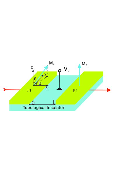
We consider a 2D ferromagnet/normal/ferromagnet junction on a strong topological insulator surface as shown in Fig. 1. The bulk ferromagnetic insulator (FI) interacts with the surface electrons in TI by the proximity effect, and the ferromagnetism is induced in the topological surface statesT.Yokoyama2010 ; B.Soodchomshom2010 ; M.Salehi2011 ; S.Mondal2010 ; J.P.Zhang2012 ; Z.Wu2010_Y.Zhang2010 ; H.Haugen2008 ; I.Vobornik2011 ; Weidong Luo2012 . The interfaces between ferromagnet (FM) and normal segment are parallel to direction, and the normal segment is located between and with gate voltage exerted on itH.Steinberg2011 ; Y.Wang2012 ; J.R.Williams2007 . Here we presume, for the simplicity, the distance between two interfaces is shorter than the mean free path as well as the spin coherence length.
With this setup, the Hamiltonian for this system readsT.Yokoyama2010 ; B.Soodchomshom2010 ; M.Salehi2011 ; S.Mondal2010 ; J.P.Zhang2012 ; Z.Wu2010_Y.Zhang2010
| (1) |
with Pauli matrices , the in-plane electron momentum , and Fermi velocity . The piecewise magnetization is chosen to be a 3D vector pointing along an arbitrary direction in the left region with , and fixed along the axis perpendicular to the TI surface in the right region with . We can use a soft magnetic insulator for the left ferromagnet, which is controlled by a weak external magnetic field, and a magnetic insulator with very strong easy-axis anisotropy for the right ferromagnet. The configuration between the left and right ferromagnets directly depends on the weak external magnetic field, where the interlayer (RKKY) exchange coupling between left and right ferromagnetsI.Garate2010 is ignored for the simplicity. In the middle segment, there is no magnetization, but instead, a gate voltage is exerted.
Solving Eq.(1), we obtain the wave function in the left region as following:
| (4) | |||
| (7) |
where the Fermi energy lies in the upper bands of Dirac cone, and . We also define as the incident angle, then , . The wave function in normal region depends on the gate voltage. If ,
| (10) | |||||
| (13) |
where with the corresponding to the upper bands and the lower bands of the Dirac cone respectively, and if ,M.I.Katsnelson2006 it becomes
| (16) | |||||
| (19) |
The wave function in the right region is:
| (22) |
with . There exists a translation invariance along the y direction, so the momentum is conserved in the three regions, and we omit the part in wave functions. These piecewise wave functions are connected by the boundary conditions:
| (23) |
which determine the coefficients A,B,C,D and F in the wave functions.
As a result, according to the Landauer-Büttiker formula S.Datta1995 , it is straightforward to obtain the ballistic conductance at zero temperature
| (24) |
where is the width of interface along the y direction, which is much larger than , and we take as , because in our case the electron transport happens around the Fermi level.
III Numerical Results and Discussions
We focus on the two cases about the electronic transport controlled by a gate voltage through this 2D topological ferromagnet/normal/ferromagnet junction. One is the conductance and the magnetoresistance when the magnetizations in the left and right FM are collinear in the z-direction, and another is the influence of the magnetization component along the x/y direction on the conductance.
III.1 The conductance and MR for collinear magnetization
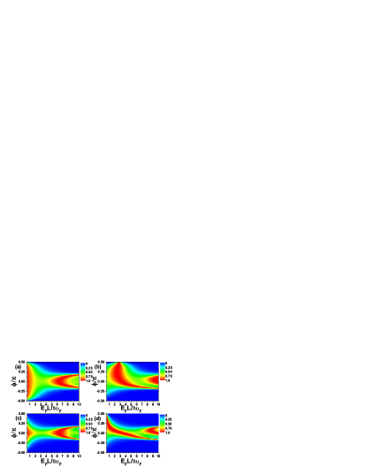
We show the normalized conductance as a function of and of parallel (Fig. a and c) and antiparallel (Fig. b and d) configurations for two different magnetizations along the z-axis in Fig. 2, where . In Figs. 2(a) and 2(b) we choose , while in Figs. 2(c) and 2(d) .
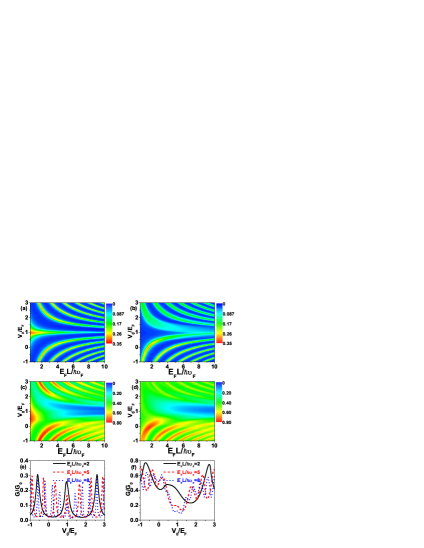
In Fig. 2(a) the gap of surface state in the left and right ferromagnet regions opened by the magnetization along the z-axis is . The conductance oscillates with the gate voltage (parameters and in Fig. 2 are dimensionless). The maximum of conductance gradually decreases as the width increases. The minimum of conductance can approach to zero. The change of conductance between maximum and minimum by gate voltage is similar to the spin field-effect transistor, in which the conductance modulation arises from the spin precession due to the spin-orbit couplingS.Datta1990 . The gate voltage can be used to change the such that the phase factor of quantum interference in the normal segment can be changed. The oscillation period of conductance with respect to depends on the width and decreases with the increase of width . The conductance has a period with respect to , when , in 2D topological ferromagnet/ferromagnet junctionT.Yokoyama2010 ; B.Soodchomshom2010 .
In Fig. 2(b), the conductance changes with the width and gate voltage in the same way as in Fig. 2(a). The difference is that the conductance is maximum in Fig. 2(b) while it is minimum in Fig. 2(a) and vice versa. The conductance in Fig. 2(c) and Fig. 2(d) show the same variation tendency with the width and gate voltage as Fig. 2(a) and Fig. 2(b), respectively. However both the maximum and minimum of conductance in Fig. 2(c) and Fig. 2(d) are larger than those in Fig. 2(a) and Fig. 2(b), since the gap of surface states in left and right ferromagnet regions is in Fig. 2(c) and Fig. 2(d). The conductance changes more obviously with the gate voltage at the side of than at the side of . In Fig. 2, both the maximum and minimum of the conductance become smaller when the gate voltage is closer to the Fermi energy, because the number of the incident wave functions transported through the normal segment by the evanescent waves (imaginary ) becomes bigger. Fig. 2 shows that the conductance of this 2D topological ferromagnet/normal/ferromagnet junction could be changed by the same way as that in the spin field-effect transistor. While for the reason of the angular spectrum of electrons in the surface plane and the linear dispersion relation, how to get a large maximum/minimum ratio of the conductance is important for a transistor.
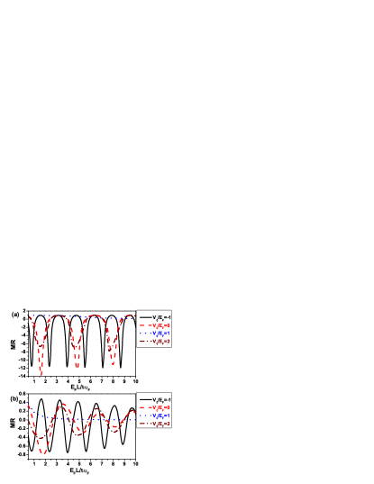
After obtaining the conductance of parallel configuration and of antiparallel configuration, we can get the MR directly, which is defined as . Compared with the conductance in Fig. 2(a) and Fig. 2(c), the conductance in Fig. 2(b) and Fig. 2(d) shows a property indicated below. On the one hand , the conductance in the antiparallel configuration can be less than that in the parallel configuration as in the conventional spin valveI.Zutic2004 ; S.A.Wolf2001 ; A.Fert2008 and its counterpart in grapheneC.Bai2008 . On the other hand, the conductance in the antiparallel configuration can also be larger than that in the parallel configuration, which is an anomalous electronic transport property of topological spin-valve junction. Fig. 3 shows the MR as a function of the width . When , the MR oscillates with the width . The amplitude and period of oscillation of MR depend on the gate voltage . When , the MR does not oscillate and decreases monotonically with the increase of , because the Fermi surface of normal segment is at the Dirac point in this case and the corresponding density of states is zero while the conductance is not zero, which is a typical property of Dirac fermion systemM.I.Katsnelson2006 . The MR could be negative for the anomalous electronic transportT.Yokoyama2010 ; T.Yokoyama2011 . The maximum of MR in Fig. 3(a) is larger than that in Fig. 3(b), and it can approach . The big negative MR (more than -10) in Fig. 3(a) also means a big variation of conductance between parallel and antiparallel configuration.
Next we will discuss the underlying physics quantitatively to understand the above results clearly. Since the electrons from all incident angles give contributions to the conductance which is proportional to the electron transmission probability, the physical origin of conductance oscillating with the width and gate voltage in Fig. 2 is a direct result of summation of electron transmission probability over all incident angles.
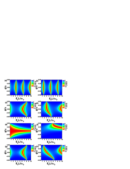
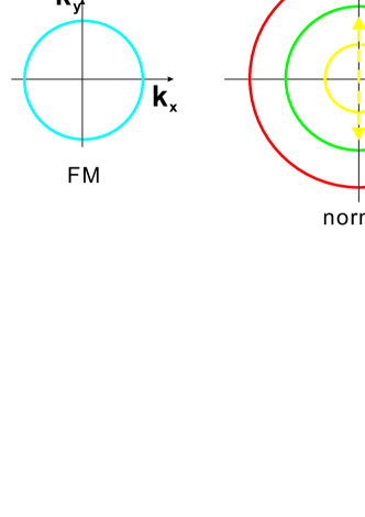
Fig. 4 plots the transmission probability as a function of incident angle and width for different gate voltage . We find that the transmission probability mainly oscillates with the width . Its period of oscillation becomes large as the gate voltage increases from to . The reason for such a change can be illustrated in Fig. 5. Because the wave functions in the left and right FMs are connected through the wave function in normal segment, the transmission probability depends on the phase factor . Due to the conservation of momentum , depends on the gate voltage. When the gate voltage from to , the Fermi surface for the normal region reduces as in Fig. 5, and reduces too, such that the transmission probability has a longer periodicity with the width and changes considerably with incident angles as shown in Fig. 4(a) or 4(b) and 4(c) or 4(d). In these cases, the electronic transport through the normal segment occurs in the upper bands of Dirac cone. Although the Fermi surface for the normal segment in Fig. 4(g) or 4(h) is equal to that in Fig. 4(c) or 4(d), their transmission probability is different, because in Fig. 4(g) or 4(h) the electronic transport through the normal segment occurs in lower bands of Dirac cone. When the gate voltage , the electronic transport through the normal segment is totally due to the evanescent waves, the transmission probability is not a periodic function of width as in Fig. 4(e) or 4(f).
Now we consider the influence of magnetization configuration on the transmission probability. It is clearly that the transmission probability is an even function of the incident angle in the parallel configuration at the left-hand side of Fig. 4, while it is not an even function of the incident angle in the antiparallel configuration at the right-hand side. This is unusual, because the transmission probability is an even function of the incident angle on the antiparallel configuration in its counterpart in grapheneC.Bai2008 . This unusual property arises from the unequal spinor parts of the incident and transmission wave functions. At the normal incidence (), the period of the transmission probability with the width L in the parallel configuration is the same as that in the antiparallel configuration and the position of maximum of the transmission probability has a shift of the half-period between two configurations. Now with the help of Figs. 4 and 5, the properties of conductance in Fig. 2(a) and 2(b) and MR in Fig. 3(a) could be understood explicitly.
When the magnetizations in the left and right FMs are taken as in Fig. 5(b), one may see that the gaps of the surface states in the left and right ferromagnet regions decrease, and the Fermi surfaces in the left and right FMs become large. So, the range of expands, and those of and the phase factor expand too. The transmission probability in Fig. 6 changes more dramatically than in Figs. 4(c) and 4(d), 4(g) and 4(h). Therefore, as the gap of surface states in left and right ferromagnet regions decreases, more incident electronic states will contribute to the conductance, such that the conductance becomes larger on the whole, and more unsymmetrical about the gate voltage in Fig. 2(c) and Fig. 2(d). The MR in Fig. 3(b) could be understood, similarly.
III.2 The influence of x/y component of magnetization on the conductance
Now we consider the influence of x/y component of magnetization on the conductance. First, we choose the z component of magnetization in the left and right FM to be equal as that in subsection A. We find that the influences of x/y component of magnetization on the conductance are quite different. The x component of magnetization has no influence on the conductance, while the y component of magnetization has a great influence on the conductance. Because the x component of magnetization just moves the Fermi surface along the x axis, the states contributing to the conductance do not change, while the y component of magnetization shifts the Fermi surface in the left FM along the y direction and decreases the number of incident electron states that contribute to the conductance.
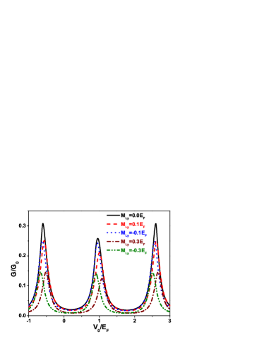
The influence of on the conductance is shown in Fig. 7. It is seen that the conductance decreases with increasing , so a large can lead the conductance to be zero. We also discover that the influence of magnetization on the conductance is different from that of .
Second, by keeping the magnetizations in the left and right FMs the same value, the direction of magnetization in the left FM is changed in the x-z plane () or in the y-z plane (), where and are indicated as shown in Fig. 1.
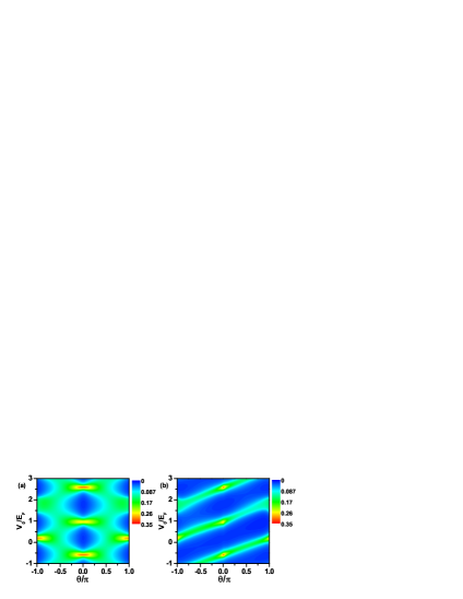
The conductance as a function of and the gate voltage is plotted in Fig. 8, which is different from that in ferromagnetic/normal/ferromagnetic graphene junctionT.Yokoyama2011 . The distinction between Figs. 8(a) and 8(b) is more obvious at , where the conductance changes slightly with the gate voltage in Fig. 8(a) while the conductance changes remarkably in Fig. 8(b). These results are from different connections of wave functions between left and right FMs. Since when , the spin in the right FM is parallel to , T.Yokoyama2010 and the spin in the left FM is parallel to in Fig. 8(a) which satisfies the relation , while the spin in the left FM is parallel to in Fig. 8(b) which satisfies the relation . In this case, the z component of spin in the left FM is in Figs. 8(a) and 8(b). Because in Fig. 8(b) the Fermi surface of left FM shifts along the y direction about , the difference of x component of spin between the left FM and right FM in Fig. 8(a) is larger than that in Fig. 8(b).
Finally, we discuss the realization of our model. The bulk band gap of topological insulator is small and depends on the materials, which is for example, about meV in , meV in H.Zhang2009 ; Y.Xia2009 ; Y.L.Chen2010 , and meV in HgTeC.Brune2011 . Far away from the Dirac point, the surface electronic states exhibit large deviations from the simple Dirac cone in Y.L.Chen2009 . The gap of surface states could be induced by putting the magnetic insulator on the surface of a topological insulator (such as EuO, EuS and MnSe). Depending on the interface match of the topological insulator and ferromagnetic insulator, the gap is several to dozens of meV T.Yokoyama2010 ; H.Haugen2008 ; I.Vobornik2011 ; Weidong Luo2012 . The gate electrode could be attached to the topological insulator to control the surface potentialH.Steinberg2011 ; Y.Wang2012 ; J.R.Williams2007 . The predicted properties of our model may be observed when the Fermi energy of surface states is about meV, and the junction width is about nm. The calculated results in this paper are based on the ballistic transport. In order to observe experimentally our predicted properties, a clean 2D topological surface states with enough long mean free path is needed. It is interesting to note that the surface of topological insulator with such a long mean free path can be realized in experimentsY.Wang2012 .
IV Summary
In summary, we have studied the electronic transport properties of the ferromagnet/normal/ferromagnet junction on the surface of a strong topological insulator, where a gate voltage is exerted on the normal segment with a finite width. It is found that the conductance oscillates with the width of normal segment and the gate voltage. The maximum of conductance gradually decreases as the width increases and the minimum of conductance approaches zero. This gate-controlled conductance behaves in the same way as the spin field-effect transistor does, but a further study is needed to increase the maximum/minimum ratio of the conductance. The magnetoresistance can be very large and could also be negative owing to the anomalous transport. In addition, when there exists a magnetization component in the 2D plane, it is shown that only the magnetization component parallel to the junction interface has an influence on the conductance.
Acknowledgements.
One of authors (KHZ) acknowledges discussions with Fei Ye and Zhe Zhang. This work is supported in part by the NSFC (Grant Nos. 90922033, 10934008, and 10974253), the MOST of China (Grant No. 2012CB932900 and 2013CB933401) and the CAS.References
- (1) M. Z. Hasan, and C. L. Kane, Rev. Mod. Phys. 82, 3045 (2010); X. L. Qi, and S. C. Zhang, ibid, 83, 1057 (2011).
- (2) C. L. Kane, and E. J. Mele, Phys. Rev. Lett. 95, 146802 (2005); 95, 226801 (2005).
- (3) B. A. Bernevig, T. L. Hughes, and S. C. Zhang, Science 314, 1757 (2006).
- (4) M. König, S. Wiedmann, C. Brüne, A. Roth, H. Buhmann, L. W. Molenkamp, X. L. Qi, and S. C. Zhang, Science 318, 766 (2007).
- (5) L. Fu, C. L. Kane, and E. J. Mele, Phys. Rev. Lett. 98, 106803 (2007).
- (6) R. Roy, Phys. Rev. B 79, 195322 (2009); J. E. Moore, and L. Balents, ibid, 75, 121306(R) (2007).
- (7) H. Zhang, C. X. Liu, X. L. Qi, X. Dai, Z. Fang, and S. C. Zhang, Nat. Phys. 5, 438 (2009).
- (8) L. Fu, and C. L. Kane, Phys. Rev. B 76, 045302 (2007).
- (9) Y. Zheng, and T. Ando, Phys. Rev. B 65, 245420 (2002).
- (10) L. Fu, and C. L. Kane, Phys. Rev. Lett. 100, 096407 (2008).
- (11) D. Hsieh, D. Qian, L. Wray, Y. Xia, Y. S. Hor, R. J. Cava, and M. Z. Hasan, Nature 452, 970 (2008).
- (12) Y. Xia, D. Qian, D. Hsieh, L. Wray, A. Pal, H. Lin, A. Bansil, D. Grauer, Y. S. Hor, R. J. Cava, and M. Z. Hasan, Nat. Phys. 5, 398 (2009).
- (13) Y. L. Chen, J. H. Chu, J. G. Analytis, Z. K. Liu, K. Igarashi, H. H. Kuo, X. L. Qi, S. K. Mo, R. G. Moore, D. H. Lu, M. Hashimoto, T. Sasagawa, S. C. Zhang, I. R. Fisher, Z. Hussain, and Z. X. Shen, Science (329) 659 (2010).
- (14) T. Zhang, P. Cheng, X. Chen, J. F. Jia, X. Ma, K. He, L. Wang, H. Zang, X. Dai, Z. Fang, X. Xie, and Q. K. Xue, Phys. Rev. Lett. 103, 266803 (2009).
- (15) J. Seo, P. Roushan, H. Beidenkopf, Y. S. Hor, R. J. Cava, and A. Yazdani, Nature 466, 343 (2010).
- (16) J. G. Analytis, R. D. McDonald, S. C. Riggs, J. H. Chu, G. S. Boebinger, and I. R. Fisher, Nat. Phys. 6, 960 (2010).
- (17) K. Eto, Z. Ren, A. A. Taskin, K. Segawa, and Y. Ando, Phys. Rev. B 81, 195309 (2010).
- (18) C. Brüne, C. X. Liu, E. G. Novik, E. M. Hankiewicz, H. Buhmann, Y. L. Chen, X. L. Qi, Z. X. Shen, S. C. Zhang, and L. W. Molenkamp, Phys. Rev. Lett. 106, 126803 (2011).
- (19) B. Xia, M. Y. Liao, P. Ren, A. Sulaev, S. Chen, C. Soci, A. Huan, A. TS. Wee, A. Rusydi, S. Q. Shen, and L. Wang, arXiv: 1203. 2997.
- (20) C. W. J. Beenakker, Rev. Mod. Phys. 80, 1337 (2008); A. H. Castro Neto, F. Guinea, N. M. R. Peres, K. S. Novoselov, and A. K. Geim, Rev. Mod. Phys. 81, 109 (2009).
- (21) S. Datta, and B. Das, Appl. Phys. Lett. 56, 665 (1990).
- (22) I. Žutić, J. Fabian, and S. Das. Sarma, Rev. Mod. Phys. 76, 323 (2004).
- (23) S. A. Wolf, D. D. Awschalom, R. A. Buhrman, J. M. Daughton, S. von Molnár, M. L. Roukes, A. Y. Chtchelkanova, and D. M. Treger, Science 294, 1488 (2001).
- (24) A. Fert, Rev. Mod. Phys. 80, 1517 (2008).
- (25) Z. G. Zhu, G. Su, Q. R. Zheng, and B. Jin, Phys. Rev. B 68, 224413 (2003); B. Jin, G. Su, Q. R. Zheng, and M. Suzuki, Phys. Rev. B 68, 144504 (2003).
- (26) H. F. Mu, Q. R. Zheng, B. Jin, and G. Su, Phys. Lett. A 336, 66 (2005); H. F. Mu, G. Su, and Q. R. Zheng, Phys. Rev. B 73, 054414 (2006); X. Chen, Q. R. Zheng, and G. Su, Phys. Rev. B 78, 104401 (2008).
- (27) T. Yokoyama, Y. Tanaka, and N. Nagaosa, Phys. Rev. B 81, 121401(R) (2010).
- (28) B. Soodchomshom, Phys. Lett. A 374, 2894 (2010).
- (29) M. Salehi, M. Alidoust, Y. Rahnavard, and G. Rashedi, Phys. E 43, 966 (2011).
- (30) S. Mondal, D. Sen, K. Sengupta, and R. Shankar, Phys. Rev. Lett. 104, 046403 (2010); S. Mondal, D. Sen, K. Sengupta, and R. Shankar, Phys. Rev. B 82, 045120 (2010).
- (31) Jinhua Gao, Wei-Qiang Chen, Xiao-Yong Feng, X. C. Xie, and Fu-Chun Zhang, arXiv: 0909. 0378v1.
- (32) J. P. Zhang, and J. H. Yuan, Eur. Phys. J. B 85, 100 (2012).
- (33) Jian-Hui Yuan, Ze Cheng, Jian-Jun Zhang, Qi-Jun Zeng, and Jun-Pei Zhang, arXiv: 1204. 0956v1.
- (34) Z. Wu, F. M. Peeters, and K. Chang, Phys. Rev. B 82, 115211 (2010); Y. Zhang, and F. Zhai, Appl. Phys. Lett. 96, 172109 (2010).
- (35) H. Steinberg, J. B. Laloë, V. Fatemi, J. S. Moodera, and P. Jarillo-Herrero, Phys. Rev. B 84, 233101 (2011).
- (36) Y. Wang, F. Xiu, L. Cheng, L. He, M. Liang, J. Tang, X. Kou, X. Yu, X. Jiang, Z. Chen, J. Zou, and K. L. Wang, Nano Lett. 12, 1170 (2012).
- (37) J. R. Williams, L. DiCarlo, and C. M. Marcus, Science 317, 638 (2007).
- (38) H. Haugen, D. Huertas, and A. Brataas, Phys. Rev. B 77, 115406 (2008).
- (39) I. Vobornik, U. Manju, J. Fujii, F. Borgatti, P. Torelli, D. Krizmancic, Y. S. Hor, R. J. Cava, and G. Panaccione, Nano Lett. 11, 4079 (2011).
- (40) Weidong Luo, and Xiao-Liang Qi, arXiv: 1208. 4638v1.
- (41) I. Garate, and M. Franz, Phys. Rev. B 81, 172408 (2010).
- (42) M. I. Katsnelson, Eur. Phys. J. B 51, 157 (2006).
- (43) S. Datta, Electronic Transport in Mesoscopic Systems(Cambridge University Press, Cambridge, 1995).
- (44) C. Bai, and X. Zhang, Phys. Lett. A 372, 725 (2008).
- (45) T. Yokoyama, and J. Linder, Phys. Rev. B 83, 081418(R) (2011).
- (46) Y. L. Chen, J. G. Analytis, J. H. Chu, Z. K. Liu, S. K. Mo, X. L. Qi, H. J. Zhang, D. H. Lu, X. Dai, Z. Fang, S. C. Zhang, I. R. Fisher, Z. Hussain, and Z. X. Shen, Science 325, 178 (2009).