Band offsets and density of Ti3+ states probed by X-ray photoemission on LaAlO3/SrTiO3 heterointerfaces and their LaAlO3 and SrTiO3 bulk precursors
Abstract
A set of (LAO-STO) interfaces has been probed by x-ray photoemission spectroscopy in order to contrast and compare the effects of LAO overlayer thickness and of the growth conditions on the electronic properties of these heterostructures. These effects are tracked by considering the band-offset and the density of Ti+3 states, respectively. It is shown that the dominant effects on the local electronic properties are determined by the O2 partial pressure during the growth. In particular, a low P(O2) yields Ti+3 states with higher density and lower binding energy as compared to the sample grown at high P(O2) or to the bare STO reference sample. Band offset effects are all below about 0.7 eV, but a careful analysis of Ti 2p and Sr 3d peaks shows that valence band offsets can be at the origin of the observed peak width. In particular, the largest offset is shown by the conducting sample, that displays the largest Ti 2p and Sr 3d peak widths.
pacs:
Valid PACS appear hereI Introduction
Lanthanum aluminate (LaAlO3, LAO in short) and strontium titanate (SrTiO3, STO) are formally band insulators, as they are closed-shell compounds (4f0 for LAO and 3d0 for STO), with a band gap of 5.4 and 3.2 eV, respectively. These materials belong to the perovskite group, sharing the same chemical formula (ABO3) and a similar cubic crystal structure. When a LAO-STO heterointerface is created, a p-type heterostructure is expected if the bulk STO is terminated with a SrO plane (hole doping), while an n-type heterostructure should be obtained with a TiO2 plane (electron doping) termination. In the latter case, the LAO-STO interface becomes conductingLAOSTO_ohtomo and yields a quasi-2D electron gas (2DEG). The transition to the metallic state was found to be thickness dependent: the 2DEG is observed only when the LAO capping is at least 4 u.c. (unit cell) thickLAOSTO_science . The main difference between LAO and STO resides in the layer charge polarityLAOSTO_rev1 : looking at the (001) planes, STO is a non-polar solid, since both Sr2+O2- and Ti4+O planes are charge-neutral, while LAO is a polar solid, as it is composed of La3+O2- and Al3+O charged layers. The p-type interface is thus formed by SrO - (AlO planes, while the n-type by TiO2 - (LaO)1+ planes. The observed conductivity was originally thought to be the response of the system to the diverging potential (the so-called polar catastrophe polarcatastrophe1 ; polarcatastrophe2 ) created by LAO.
In non-oxide semiconductors, the relaxation of polar discontinuity in heterointerfaces is usually achieved by an atomic reconstruction processLAOSTO_ohtomo , where the interface stoichiometry is altered by interdiffusion, point defect, dislocation and in general by a structural roughening. In oxides, the possibility of multiple valence ions allows also an electronic reconstruction that, in LAO-STO case, should move electrons from the surface to the empty Ti d levels, leading to 3d1 electronic states. A 2D lattice of electrons in a correlated material can originate phenomena like MIT transitions, localized magnetic moments and even superconductivity LAOSTO_rev2 ; LAOSTO_rev3 ; most of these effects have been observed in LAO-STO, though not all in one sample at the same time.
In principle, both atomic and electronic reconstruction could be present in the LAO-STO case. For example, there are many experimental proofs of interdiffusion LAOSTO_chambers ; VONK (with La ions drifting inside STO, a form of atomic reconstruction), but this mechanism alone cannot be solely responsible of the conductivity, since in principle it should be present also in the p-type interface. On the other hand, standard polar catastrophe (an electronic reconstruction picture) was invoked to explain the lack of conductivity for thickness below 4 u.c, but a discrepancy exists between the theoretically expected and the measured band bending effects. In fact, the thickness dependence of conductivity could be explained by a band bending effectBandBending , induced by polarity discontinuity: the density of states (DOS) of LAO valence band (VB) should be shifted to higher binding energies till, for a capping equal or major of 4 u.c., the VB maximum is superimposed to the buried empty levels of STO. The conduction should be now triggered by a tunneling effect from the surface to the interface. However, a significant band bending has not yet been observed in terms of core-level shift, while a shift of 3.2 eV (needed to span the electronic gap in STO) should be easily observed.
Finally, the sample growth conditions deeply affect the transport properties; an oxygen-poor growth atmosphere can induce oxygen vacancies and thus a 3D conductivityOxyVac1 ; OxyVac2 ; OxyVac3 ; OxyVac4 , while an excessively-rich one can even result in a 3D growth and thus in a different kind of heterostructureLAOSTO_rev2 . Depending on the O2 partial pressure during growth, three phases are usually identified, LAOSTO_rev3 ; LAOSTO_natmat : one dominated by oxygen vacancies contribution (P mBar), one displaying superconductivity (P mBar) and one displaying a magnetic behavior (P mBar). It is quite a challenging task to find a unified description of all these phenomena.
The experimental signatures of many of the proposed models are the LAO-STO band offset, and the density and distribution of Ti3+ states. Recently, these states have been evidenced by soft X-ray photoemission with photon energy tuned at the Ti 2p-3d threshold APL_LAOSTO ; KOI_2011 . Also core level XPS can provide an indication of Ti3+ states as reported in Ref.KOI_2011 ; fuji_2011 and in hard X-ray photoelectron spectroscopy (HAXPES) experiments LAOSTO_haxpes . At odds with Ref.KOI_2011 ; fuji_2011 ; APL_LAOSTO , Ref.LAOSTO_chambers did not report on observed Ti3+ features in Ti 2p core level photoemission.
As for valence band offsets (VBO), core level shifts much smaller than those predicted by the polar catastrophe have been observed by Takizawa et al.fuji_2011 , Chambers et al. LAOSTO_chambers and Segal et al. segall but it is not yet possible to draw a consistent picture of VBO as the results show in some cases opposite trends.
In the present study, a spectroscopic investigation of insulating and conductive LAO-STO films is carried out by X-ray Photoelectron Spectroscopy (XPS). We address the problem of the spectroscopic signature of the interface effects by comparing several LAO-STO interfaces with their LAO and STO bulk precursors. We checked to which extent the electronic properties of LAO-STO can be described as a weighted (i.e. thickness dependent) superposition of those of LAO and STO, as deviations from this mere superposition should be regarded as a signature of new electronic states arising from the heterointerface build-up.
Following this approach, we show that the different LAO overlayer thicknesses affect the electronic properties of the interfaces in terms of band-offsets, though smaller that those theoretically predicted, whereas the dominant effects on the local electronic properties are related to the O2 partial pressure during the growth. This is seen by tracking the Ti3+/Ti4+ ratio for Ti 2p core levels, and the Sr 3d and Ti 2p core level line widths. Though band offsets are all below about 0.7 eV, differences are detected among the samples and it is shown that the Ti 2p and Sr 3d peak widths scale with band offsets, the larger values being found for the 5 u.c. conducting sample. Finally, a careful analysis of the Ti3+/Ti4+ peak area ratio based on the depth distribution function of photoelectrons, allowed us to set a lower limit to the density of Ti3+ states across the interface as seen by the present photoemission experiment.
II Experimental details
The LAO-STO heterostructures (HS) have been grown by pulsed laser deposition at the MESA+ Institute for Nanotechnology, University of Twente. The two n-type 3 u.c. and 5 u.c. LAO-STO samples were grown in a P mBar oxygen partial pressure. In addition, an insulating n-type 5 u.c. LAO-STO sample, grown at 10-1 mBar O2 partial pressure has been analyzed. Two reference single-crystal LAO and STO samples terminated with the (001) surface have also been considered (MaTeck GMBH). The sample list is reported in Table I. XPS has been used to measure the core-level electronic structure and to evaluate the stoichiometry of the heterostructures. The XPS data have been collected at the Surface Science and Spectroscopy Lab of the Università Cattolica (Brescia, Italy) with a non-monochromatized dual-anode PsP x-ray source; the Mg kα line (=1253.6 eV) has been used to achieve a better resolution (about 0.7 eV), while the Al kα line (=1486.6 eV) has been used when the maximum probing depth was needed. The analyzer for XPS was a SCIENTA R3000, operating in the transmission mode, which maximizes the transmittance and works with a 30° acceptance angle.
In XPS, the core-level peak area of a selected layer at a depth with a thickness can be evaluated through the following formula:
| (1) |
where K is a normalization constant, which includes the photoionization cross section, the atomic density of the species and analyzer-dependent parameters; is the generical escape probability (known as depth distribution function, DDF) of an electron generated at a depth with a kinetic energy at an angle respect to the surface normal.
According to the Lambert-Beer law, the DDF function is usually approximated with a Poisson distribution , where is the inelastic mean free path (IMFP). Even if it leads to simple analytical expressions for the peak areas, such approximation (defined as straight line motion by Tilinin et al.TilinDDF ), is known to be quantitatively wrong and, especially for the present thin overlayers, can results in an overestimated capping thickness.
In this work, we resorted to Monte-Carlo (MC) DDF calculations, with the algorithm described in Ref.WernerDDF , in order to include inelastic as well as elastic electronic scattering, in the so-called transport approximationJablonskiTA (TA). The photoemission asymmetry parameters have been taken into account for each core-level. Monte-Carlo calculations of electron trajectories have been carried out in order to predict the XPS peak areas in LAO-STO heterostructures, since an analytic DDF formulationTilinDDF can not be written for a generic multilayer sample.
III Results and Discussion
III.1 Core level and valence band photoemission
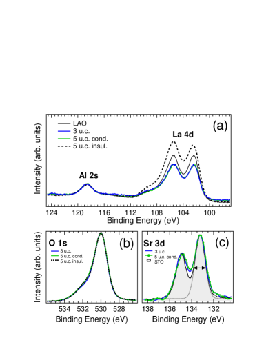
The La 4d and Al 2s XPS shallow core levels are shown in Fig.1-a. All spectra are normalized to the Al 2s peak. As can be observed, for the the 5 u.c. conducting and the 3 u.c. insulating samples the La 4d core levels are superposed, with an intensity below that of the LAO reference crystal. In turn, the La 4d XPS core lines of the 5 u.c. insulating sample display the largest intensity. These features are qualitatively consistent with the results reported in literatureQIAO2011 , and suggest that the P(O2) value has a relevant effect on the cation stoichiometry in the LAO overlayer. This is not unexpected, as the 5 u.c. insulating sample is known to show a 3D growth regime rather than the layer-by-layer regime for the other two heterostructures grown at lower P(O2). It has been observed QIAO2011 that among possible defects related to a La excess with respect to Al, the formation of Al vacancies seems to be the most likely scenario. In turn, the low La intensity of the heterostructures grown at low P(O2) as compared to the case of the LAO single crystal, apparently shows a La deficiency that can be related to La diffusion through the interface, La substoichiometry, or both.
The O 1s spectra from the three heterostructures are shown in Fig.1-b. It is important to note that the three spectra are virtually identical, in spite of the different growth conditions and thickness of the LAO overlayer. This assures that in all cases a similar oxygen stoichiometry can be estimated at the surface, ruling out the possibility that changes at the interface could be ascribed to major differences in the oxygen stoichiometry on the surface.
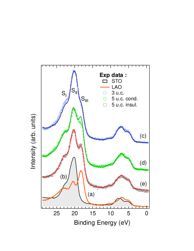
In Fig.2 the valence band (VB) spectra, collected with the Mg kα x-ray source, are shown. The shallow core levels are labeled as SI, SII and SIII. The O 2s states mostly contribute to the SI peak, Sr 4p is an unresolved doublet below SII peak and La 5p is split in SII and SIII peaks (the spin orbit energy separation is about 2.4 eV, as detected in, e.g., in La2O3 La2O3 ). It is possible to describe the LAO-STO spectra as the linear combination of the single-crystal spectra. Starting from the LAO and STO spectra as displayed in Fig.2, the VB of the three LAO-STO samples have been calculated as a linear combination of the bulk precursor spectra where two fitting parameters have been considered, i.e. the energy shift of the LAO VB spectrum with respect to the STO VB spectrum, and the relative integrated intensity of these two VB spectra. The results of this procedure are shown in fig.2, thin lines. In all cases, there is a slight difference (below 0.2 eV) among the energy shifts resulting from the best fit of the three LAO-STO interfaces (Table II: LAO vs. STO BE shift). If band bending is present, such a small difference is unable to be the sole cause of the build-up of the 2DEG.
| P(O2) | Ti3+/Ti4+ | (BE) | Ti2p | Sr 3d | SCD | SCD | ||
| mbar | XPS | Ti4+-Ti3+ | FWHM | FWHM | (Ti 2p) | 1 u.c. | 2 u.c. | |
| x 10-3 | ratio | (eV) | (eV) | (eV) | (eV) | |||
| 5 u.c. cond. | 1.0 | 0.056 | 2.03 | 1.47 | 1.24 | 0.56 | 1.50x10¹⁴ | 1.68x10¹⁴ |
| 3 u.c. ins. | 1.0 | 0.012 | 2.10 | 1.43 | 1.18 | 0.44 | 3.70x10¹³ | 4.00x10¹³ |
| 5 u.c. ins. | 100 | 0.006 | 1.78 | 1.41 | — | 0.37 | — | |
| — | 0.004 | 1.73 | 1.36 | 1.05 | 0.00 | — |
On the intensity side, the accuracy of the fitting results can be checked by evaluating if the STO signal attenuation obtained from the fitting is consistent with the thickness of the LAO overlayer. Defining the integrated intensity of the XPS signal referred to STO as , then the STO signal attenuation of the 5 u.c. (thickness = d5) sample with respect to the 3 u.c. (d3) sample can be written as
| (2) |
while this ratio is experimentally determined to be about 0.59 for the two sample grown at low P(O2). Solving the equation to extract the thickness difference between the two layers, a value of Å is obtained, in good agreement with the expected 5-3=2 u.c. thickness (7.6 - 7.8 Å). This makes the signal attenuation evaluated from the VB and shallow core levels consistent, providing also a positive feedback on the results about the negligible LAO-STO valence band offset among the samples. It is also worth noting that the measured peak SIII, ascribed to La 5p3/2, in the 5 u.c. conducting sample (Figure 2-d) is lower than the calculated peak. This is consistent with the fact the this sample has been evaluated as La poor from the shallow core level analysis (Fig.1). Finally, we observe that the use of the inelastic mean free path alone rather than the DDF, would yield a Å value, clearly in contrast with the expected thickness. This further shows the inadequacy of the IMFP concept in the estimation of attenuation lengths.
III.2 Binding Energy shifts and band offsets
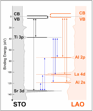
Possible band offsets can also be measured by considering the BE difference between a core line from a LAO element and a core line of an STO element. Following Ref. LAOSTO_chambers , we have evaluated the following differences (Eq. 3 to 8):
| (3) | ||||
| (4) | ||||
| (5) | ||||
| (6) |
| (7) | ||||
| (8) |
that can be identified by referring to the diagram of Fig.3, where the energy levels involved in the calculations for both the reference LAO and STO single crystals and the LAO-STO heterostructure are shown. The results are reported in Table II. As can be observed, when averaged over the six different combinations, all differences are within 0.15 eV (Table II: ave. core), in agreement with the results obtained from the VB data analysis (0.21 eV; Table II: LAO vs. STO BE shift).
Several studies on the band lineup have been published so far, but it is rather difficult to find a rationale among them. A first group of studies is focussed on core level differences between p-type and n-type samples. Takizawa et al. fuji_2011 have focussed on the band lineup of p-type and n-type interfaces, both with 1,3,4,5, and 6 LAO u.c. overlayers. They show that core levels belonging to the same layer of the HS (i.e. La and Al for LAO, and Ti and Sr for STO) do not show appreciable shifts (less than 100 meV). In turn, an energy shift is observed for the Al2p-Sr3d BE difference. This shift increases with the number of LAO u.c. for both p and n-type samples. The interfaces have been grown by PLD in a 1x10⁻⁵ torr oxygen partial pressure. Segal et al. segall present a similar study, where p-type and n-type interfaces with 2 up to 9 LAO u.c. have been investigated and the Sr3d-La4d BE difference has been tracked. Here, this energy difference is found to change with the number of layers but while it increases for p-type samples, it decreases for n-type samples. The samples have been grown by MBE in 3x10⁻⁷ torr oxygen partial pressure. Yoshimatsu et al. yoshi08 investigate the Ti 2p BE shift for both p-type and -type samples (0 to 6 LAO u.c., LPLD, torr). In this case, the Ti 2p BE for the p-type samples is found to be constant, while for the n-type samples the BE decreases with LAO thickness.
Unlike the papers so far mentioned, Chambers et al. LAOSTO_chambers did not consider the p-type and n-type set of samples, but focussed on two 4 u.c. n-type samples grown at rather similar O2 pressures (1x10⁻⁵ Torr and 8x10⁻⁶ Torr). A set of BE differences have been evaluated, namely Sr 3d - La 4d, Sr 3d- Al 2p, Ti 2p - La 4d, and Ti 2p - Al 2p. Furthermore these differences were referenced to the VBO, a procedure neglected in the previous studies. The present study follows this pathway, but important differences emerge with respect to Chamber’s results. It is rather interesting to note that in the samples considered in Ref.LAOSTO_chambers the Ti3+ contribution is not detected on the low-BE of the Ti 2p3/2 XPS peak. In the samples presented here we detect Ti3+ states in Ti 2p core lines, which find a counterpart in the 3d1 electron emission in the valence band region already probed by resonant photoemission (RESPES) in a previous investigation APL_LAOSTO . Furthermore, while Chambers detects similar BE energy differences in the same sample, irrespectively of the couple of atoms selected, we detect much different changes within the same sample. When Ti is involved as one of the core levels in Eq. 5-7, larger shift are usually detected with respect to those resulting from Eq.3, 4, and 8. This seems to indicate that in our sample it is possible to observe element specific shifts, while in the samples examined by Chambers the shift are rather uniformly distributed. This is tentatively ascribed to the fact that localized Ti3+ states at the interface may have much larger effects on the local electronic properties than the widespread charge distribution invoked by Chambers to justify the lack of Ti3+ low-BE feature in Ti 2p XPS spectra.
| La4d5/2-Sr3d | Al2s-Sr3d | La4d5/2-Ti3p | Al2s-Ti3p | Al2p-Ti3p | Al2p-Sr3d | ave. | LAO vs STO | |
|---|---|---|---|---|---|---|---|---|
| core | VB shift | |||||||
| 5 u.c. cond. | -0.46 | -0.54 | -0.89 | -0.97 | -0.94 | -0.52 | -0.72 0.24 | -0.04 |
| 3 u.c. ins. | -0.56 | -0.61 | -0.74 | -0.79 | -0.75 | -0.57 | -0.67 0.10 | -0.10 |
| 5 u.c. ins. | -0.34 | -0.27 | -1.01 | -0.94 | -0.77 | -0.10 | -0.57 0.38 | +0.17 |
III.3 Ti 2p core levels
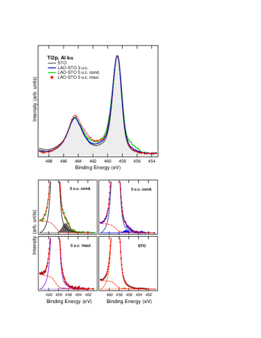
In Fig.4 the Ti 2p XPS core lines of the 3 u.c., the two 5 u.c. heterointerfaces and the pure STO are shown. The Ti 2p spectrum is almost identical to that expected for a Ti4+ ion. However, a small bump is detectable on the low BE side of the 5 u.c. spectrum, in the position usually associated to Ti3+ electronic states. These states can be detected only through a comparison among different samples and can be easily confused as an additional experimental broadening of Ti 2p3/2 peak. For this reason we also show the Ti 2p core line of SrTiO3, measured with the same energy resolution. The Ti 2p3/2 peak FWHM of the 5 u.c. conducting compound (1.47 eV) is larger than those of the 5 u.c. (1.41 eV) and the 3 u.c. (1.43 eV) insulating compounds. It is important to note that the narrower Ti 2p peak is that of STO (1.36 eV). Therefore, we see an overall decrease of the Ti 2p FWHM from the conducting LAO-STO to the insulating STO single crystal. We exclude broadening effects due to charging, which should be opposite to those observed, and therefore we regard the broadening as due to an intrinsic effect. Also the peak area of Ti3+ states of the conducting compound is larger than that of the two insulating compounds. The Ti3+/Ti4+ ratio sharply decreases from 0.056 (5 u.c.) to 0.012 (3 u.c.) and is nearly negligible for the 5 u.c. insulating sample (0.006) and the STO single crystal (0.004), assuming an uncertainty of 0.005 on the peak ratio values. Furthermore, also the Ti3+ BE of the samples grown in low P(O2) is different from that measured for the other samples, the insulating 5 u.c. and the reference STO single crystal. This peak is found about 2 eV below the main line, but this difference is reduced when the 5 u.c. insulating (1.78 eV) and the STO (1.73 eV) samples are considered, indicating a different origin for these peaks. Indeed, an insulating sample has been reportedKOI_2011 to show a Ti3+ peak closer to the main line with respect to a conducting LAO-STO interface.
The presence of Ti3+ states was controversial in early studies on LAO-STO, as not all authors observed these features in spite of the conducting nature of their samples. As already mentioned, a signature of Ti3+ states is the feature appearing on the low BE side of the Ti 2p3/2 core line. In addition, this feature should have a counterpart in the valence band region, detectable either through RESPES at the Ti L-edge, or through UPS photoemission siemo07 . While Takizawa fuji_2011 and Yoshimatsu yoshi08 discuss the properties of Ti 2p core lines, in Segal’s study segall no mention is done on Ti 2p. Yoshimatsu et al. do not report on the Ti3+ contribution, but they focus on the BE shift of the Ti 2p3/2 core line, while Takizawa et al. discuss the Ti4+/Ti3+ ratio, but do not report on Ti 2p3/2 BE shift. Furthermore, unlike more recent studiesKOI_2011 ; APL_LAOSTO , Yoshimatsu et al. do not find any evidence of 3d1 states in RESPES experiments at the Ti L-edge resonance. For the present samples, evidence of Ti 3d states in the gap are provided in Ref. drera2012 , Par.5.4.2.
In addition to Ti 2p, also the Sr 3d core levels of the heterostructures appear to be different from those of STO (Figure 1-c). As shown in Table II, in spite of the high quality of the STO side of the heterojunction, the Sr peaks are not as sharp as pristine STO. The Sr 3d peak of the conducting 5 u.c. sample 1.24 eV) is larger than that of the corresponding 3 u.c. layer 1.18 eV), both being larger than the peak measured for STO 1.05 eV). This trend is consistent with that measured for the Ti 2p core lines, suggesting the presence of disorder (cationic exchange or oxygen vacancies) around strontium atoms at the interface. This structural disorder is supposed to alter the ideal structural environment around the Ti and Sr cations, yielding potential fluctuations that ultimately may results in a Ti 2p and Sr 3d peak width broadening. Similar effects have been observed in, e.g., the Ti 2p core lines of Fe-doped rutile single crystals ironrutile .
An alternative picture to be considered, that is however supported by a qualitative analysis, is based on possible band bending effects on the peak width. Segal et al have considered this hypothesis and they have been able to estimate a band bending smaller than that expected from theoretical predictions. Indeed, Segal et al have investigated these effects on the La 4d3/2 peak width, obtaining quite smaller broadening with respect to those expected from the polar catastrophe theory. Furthermore they do not find a specific trend in the FWHM, as the data appear to be scattered.
In the present study we choose to address this question on the elements (Sr and Ti) of the buried interface. Assuming that the increase of peak width is due to band bending, it is interesting to relate the observed FWHM with the VBO by comparing the results of Table I and Table II. Here, the Ti 2p peak width in STO (1.36 eV) is regarded as the width of the ”ideal” Ti-terminated STO without the LAO capping layer. Based on this, we can extract the extra width ( ) due to the interface effects on the basis of the following Equation: . The results are reported in Table I. As can be observed, shows a decrease similar to that found for the average core level shift that appears in Table II. This indicates that larger average core level shifts yield larger Ti 2p peak widths.
Finally, from the Ti3+/Ti4+ intensity ratio, by properly considering the attenuation of the Ti signal due to the LAO overlayer, an estimation of the sheet charge density (SCD) can also be provided.
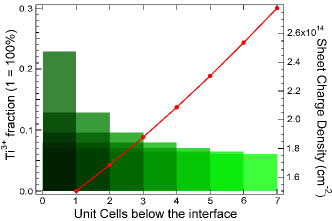
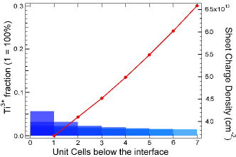
The evaluation of the Ti3+/Ti4+ ratio has been drawn on the basis of the DDF concept, using the XPS peak area values reported in Table I. The results are shown in Fig.5. Our calculations are based on the fact that the Ti3+/Ti4+ ratio reported in Table I can be generated by different distributions of the Ti3+ ions below the interface, e.g. the same ratio can be produced by a high density of ions close to the interface or by a low density of ions distributed across a larger layer below the interface. We start our analysis by assuming that, once the width of the charge profile is established, the Ti3+ ion distribution is constant below the interface. A different profile, e.g. a charge profile decaying with depth below the interface, can be ultimately described by a linear combination of constant charge profiles, as our calculation is carried out on the quite fine discrete steps (i.e. the thickness of a unit cell).
In Fig.5 the height of the histogram bars represent the Ti3+ fraction predicted for a uniform distribution of Ti3+ atoms in a layer below the interface as thick as the width of the histogram bar. The thickness of this layer is assumed to be a multiple of the STO unit cell parameter. The corresponding sheet charge density (SCD) is evaluated for each histogram bar and is shown as a thick line (right axis). Assuming that al the Ti3+ ions are located in the first unit cell below the interface, the resulting SCD is 1.5x1014 cm-2. This value represents the lowest limit for the SCD calculated on the basis of the experimental Ti4+/Ti3+ XPS peak area ratio.
A much lower estimation of the sheet charge density is drawn for the insulating 3 u.c. sample. In this case, the lowest limit for the SCD is 3.7x1013 cm-2. This value can be regarded as the intrinsic density of carries at the interface for the two samples grown al low P(O2), which is found independently on the physical mechanisms at the basis of the 2DEG build-up. If we consider a constant charge density spread about 2 u.c. below the interface, the present results are in good agreement with those reported by Sing et al. on the basis of HAXPES experiments LAOSTO_haxpes . In both cases, the estimated SCD of the conducting interface (2x10¹⁴ ) is higher than that typically obtained from transport measurements on conducting LAO-STO interfaces (about 2-6 x10¹³) LAOSTO_science ; dubroka . The SCD resulted to be high also for the 3 u.c. sample (about 4x10¹³). This discrepancy seems to point out that only a fraction of the Ti3+ states detected by XPS contribute to the 2DEG. One explanation can be found in a Ref.seo , where a distinction between two kind of charge carriers is provided: low density high mobility carriers for the transport measurements and high density low mobility carriers from optical measurements. Alternatively, the formation of photoinduced charge carriers either by X-ray or ambient light irradiation has to be considered. However, under this assumption, it is not straightforward to explain the lack of such large photoinduced effects in the insulating 3 u.c. sample and also in STO. In particular, as these effects should occur on the STO side of the junction to yield Ti3+ electronic states, it is difficult to justify the lower density for the 3 u.c. sample, where irradiation effects are supposed to be larger than in the 5 u.c. sample due to the thinner LAO overlayer on top of the STO substrate. Finally we observe that an estimate of Ti3+ fraction carried out with the IMFP attenuation length alone, without considering the full DDF approach, would overestimate the Ti3+ fraction, as neglecting, e.g., the elastic scattering events, the resulting attenuation length is higher. Namely, by using the IMFP for STO (=21.67 at KE= 1000 eV) we would obtain a Ti3+ fraction of 0.34 rather than 0.23 for a distribution depth of 1 u.c., and 0.19 rather than 0.12 for a distribution depth of 2 u.c., i.e. an overall overestimation of about 50 percent. This would yield an analogous overestimation of the SDC.
IV Conclusions
Far from being thoroughly assessed in the literature, the spectroscopic signature of 2DEG in LAO-STO interfaces is discussed in the present study, where we add novel data to the set of experiments so far reported. Indeed, rather than focussing on the difference between p-type and n-type samples, we choose to focus on oxygen stoichiometry effects and on the comparison with parent LAO and STO compounds. Unlike previous studies, we show that in LAO-STO heterostructures (i) the Ti3+ contribution to Ti 2p core levels, (ii) the Ti 3d1 in-gap states drera2012 , and (iii) larger Ti 2p width with respect to STO, can be simultaneously present, though at different extent, suggesting that all these signatures of the 2DEG are accessible via photoemission on each sample.
Three LAO-STO interfaces have been analyzed by X-ray photoemission spectroscopies, plus a LAO and STO reference single crystals. The energy, width and intensity of core level peaks, and the valence band spectra have been carefully considered in order to look for band-bending effects at the heterointerface and probe the dependence of the Ti3+ charge density on the growth conditions.
In the analysis of VBO, we consider the approach suggested by Chambers et al. LAOSTO_chambers by referencing the BE also to separated LAO and STO valence band maxima. Unlike the reported findings, we find BE differences sensitive to the choice of elements, which suggests that different atoms in the interface may undergo different energy shifts. In particular, when Ti is involved the major differences are estimated.
From the analysis of core level energies, we exclude the presence of band bending effects larger than about 0.7 eV, ruling out tunneling from the LAO offset valence band to STO empty 3d levels as the sole mechanism for the build-up of the 2DEG. Differences in band offset among the three samples are quite limited, spanning a range of about 0.2 eV, in spite of the remarkably different growth conditions and electrical properties. Likewise, differences among relative BE shift required to best-fit the LAO-STO valence band are small. However, a correlation among these differences, the peak width of Ti and Sr at the interface, and band bending is found, showing that band offset is at work to shape the energy landscape and that it is possible to consistently single out these effects by a careful analysis of spectroscopic data. Indeed,the FWHM of the Ti 2p and Sr 3d core lines is larger for the conducting sample with respect to any of the insulating interfaces and the STO single crystal. The intrinsic origin of this width is ascribed to band bending effects, though disorder effects (electronic or structural) around the photoemitting atom in the conducting sample may by at work at the same time.
Finally, we have shown that the density of Ti3+ levels strongly depends both on the LAO overlayer thickness and oxygen partial pressure during the growth. Two heterostructures grown at the same P(O2) present a well detectable Ti3+ peak about 2 eV below the Ti4+ main line. The STO and the 5 u.c. insulating samples show a much weaker contribution of Ti3+ states, with also a different binding energy. On the basis of the Ti3+/Ti4+ XPS peak area ratio, a SCD larger than that expected from transport measurements has been evaluated for the two samples grown at low P(O2), the SCD of the 5 u.c. layer being about an order of magnitude larger than in the 3 u.c. sample.
V Acknowledgments
Support from the Dutch FOM and NWO foundations is acknowledged.
References
- (1) H. Y. Hwang and A. Ohtomo, Nature 427, 423 (2004).
- (2) S. Thiel, G. Hammer, A. Schmehl, C. W. Schneider, J. Mannhart, Science 313 (2006), 1942
- (3) R. Pentcheva and W. E. Pickett, J. Phys.: Cond. Mat. 22, 043001 (2010).
- (4) N. Nakagawa, H. Y. Hwang, and D. A. Muller, Nature Mater. 5, 204 (2006).
- (5) J. Gonjakowski, F. Finocchi, and C. Noguera, Rep. Prog. Phys. 71, 016501 (2008).
- (6) N. Reyren, S. Thiel, A. D. Caviglia, L. Fitting Kourkoutis, G. Hammerl, C. Richter, C. W. Schneider, T. Kopp, A. S. Rüetschi, D. Jaccard, M. Gabay, D. A. Muller, J. M. Triscone, and J. Mannhart, Science 317, 1196 (2007).
- (7) A. Brinkman, M. Huijben, M. van Zalk, J. Huijben, U. Zeitler, J.K. Maan, W.G. van der Wiel, G. Rijnders, D.H.A. Blank and H. Hilgenkamp, Nature Materials 6, 493 (2007).
- (8) S. A. Chambers, M. H. Englehard, V. Shutthanandan, Z. Zhu, T. C. Droubay, T. Feng, H. D. Lee, T. Gustafsson, E. Garfunkel, A. Shah, J. M. Zuo, and Q. M. Ramasse, Surf. Sci. Rep. 65, 317 (2010).
- (9) V. Vonk, J. Huijben, D. Kukuruznyak, A. Stierle, H. Hilgenkamp, A. Brinkman, and S. Harkema, Phys. Rev. B 85, 045401 (2012)
- (10) R. Pentcheva and W. E. Pickett, Phys. Rev. Lett. 102, 107602 (2009).
- (11) A. S. Kalabukhov, et al., Phys. Rev. Lett. 103, 146101 (2009)
- (12) G. Herranz, et al., Phys. Rev. Lett. 98, 216803 (2007).
- (13) W. Siemons, et al., Phys. Rev. Lett. 98, 196802 (2007).
- (14) M. Basletic, et al., Nat. Matter. 7, 621-625 (2008).
- (15) G. Rijnders and D. H. A. Blank, Nature Materials 7, 270 (2008).
- (16) G. Drera, F. Banfi, F. Federici Canova, P. Borghetti, L. Sangaletti, F. Bondino, E. Magnano, J. Huijben, M. Huijben, G. Rijnders, D. H. A. Blank, H. Hilgenkamp, and A. Brinkman, Appl. Phys. Lett. 98, 1 (2011).
- (17) A. Koitzsch, J. Ocker, M. Knupfer, M. C. Dekker, K. Dörr, B. Buchner, P. Hoffmann, Phys. Rev. B 84, 245121 (2011)
- (18) M. Takizawa, S. Tsuda, T. Susaki, H. Y. Hwang, and A. Fujimori, Phys. Rev. B, 84, 245124 (2011)
- (19) M. Sing, G. Berner, K. Goss, A. Muller, A. Ruff, A. Wetscherek, S. Thiel, J. Mannhart, S. A. Pauli, C. W. Schneider, P. R. Willmott, M. Gorgoi, F. Schafers, and R. Claessen, Phys. Rev. Lett. 102, 176805 (2009).
- (20) Y. Segal, J.H. Ngai, J. W. Reiner, F. J. Walker, C. H. Ahn, Phys. Rev. B 80, 241107 (2009)
- (21) W. S. M. Werner, Surf. Int. Anal. 31, 141 (2001).
- (22) A. Jablonski, Phys. Rev. B 58, 16470 (1998).
- (23) I.S. Tilinin, A. Jablonski, J. Zemek ,S. Hucek J. Electr. Spec. Rel. Phen. 97, 127-140 (1997)
- (24) J. J. Yeh and I. Lindau, Atomic Data and Nuclear Data Tables 32, 1-155 (1985).
- (25) L. Qiao, T.C.Droubay, T. Varga, M.E. Bowden, V. Shutthanandan, Z. Zhu, T.C. Kaspar, S.A. Chambers, Phys. Rev. B 83, 085408 (2011)
- (26) M.F. Sunding, K. Hadidi, S. Diplas, O.M. Lvvik, T.E. Norby, A.E. Gunns, Journ. of Electr. Spectr. and Rel. Phen. 184, 399 (2011).
- (27) K.Yoshimatsu, R. Yasuhara, H. Kumigshira, and M. Oshima, Phys. Rev. Lett. 101 , 026802 (2008)
- (28) W. Siemons, G. Koster, H. Yamamoto, T. H. Geballe, D. H. A. Blank, M. Beasley, Phys. Rev. B 76, 155111 (2007)
- (29) G. Drera, arXiv:1210.8000 [cond-mat.str-el]
- (30) L. Sangaletti, M.C. Mozzati, G. Drera, P. Galinetto, C.B. Azzoni, A. Speghini, M. Bettinelli, Phys. Rev. B 78, 075210 (2008)
- (31) A. Dubroka et al., Phys. Rev. Lett. 104, 156807 (2010)
- (32) S. S. A. Seo, Z. Marton, W. S. Choi, G. W. J. Hassink, D. H. A. Blank, H. Y. Hwang, T. W. Noh, T. Egami, and H. N. Lee, Appl. Phys. Lett. 95, 082107 (2009);