Nonlinear Transport through ultra-narrow Zigzag Graphene Nanoribbons: non-equilibrium charge and bond currents
Abstract
The electronic nonlinear transport through ultra narrow graphene nanoribbons (sub-) is studied. A stable region of negative differential resistance (NDR) appears in the I-V characteristic curve of odd zigzag graphene nanoribbons (ZGNRs) in both positive and negative polarity. This NDR originates from a transport gap inducing by a selection rule which blocks electron transition between disconnecting energy bands of ZGNR. Based on this transition rule, on/off ratio of the current increases exponentially with the ribbon length up to . In addition, charging effects and also spatial distribution of bond currents was studied by using non-equilibrium Green’s function formalism in the presence of e-e interaction at a mean field level. On the other hand, we also performed an ab initio density functional theory calculation of transmission through a passivated graphene nanoribbon to demonstrate robustness of the transport gap against hydrogen termination of the zigzag edges.
pacs:
73.23.-b,73.63.-bI Introduction
Graphene is a two-dimensional carbon which has been recently explored novoselov . Experiments in graphene-based devices experiment have shown the possibility of controlling their electrical properties by the edge structure and also application of an external gate voltage. Nowadays, by using a chemical methodDai , it is possible to fabricate field effect transistor graphene nanoribbons (GNRs) with ultra narrow widths and smooth edges which are possibly well defined zigzag or armchair edge structures. A useful transport gap is opened in sub- GNRs at room temperature which results in a high on/off current switching up to . The origin of the transport gap can be understood by two factors: suppression of transport due to edge disorder leading to Anderson localization, confinement along transverse directionhan ; Molitor . Additional to these factors, in ultra narrow zigzag graphene nanoribbons (ZGNR), flow of current is also blocked by the symmetric selection rules cheraghchi1 ; grosso ; beenaker ; P-Ngraphene ; duan ; kurihara ; Wakabayashi .
Negative differential resistance esaki in nanoelectronic devices has been also observed in the metallic nanotube junctions farajian and in the case of potential barriers in graphene sheetsNDRgraphene .
In this paper, to shed light on the experimental work in Ref.[Dai, ], we study non-linear transport in odd zigzag graphene nanoribbons by using non-equilibrium Green’s function formalism (NEGF). It is shown that a stable NDR against electrostatic interaction up to is appeared in ultra narrow ZGNRs around in both positive and negative polarity, where is hopping integral between carbon atoms. On-off ratio of this NDR increases exponentially with the ribbon length. The NDR phenomenon occurs in far-from-equilibrium regime.
Although parity is not conserved in odd ZGNRs, current reduction is induced by an other selection rule in which transition between disconnecting band groups is forbidden (Cresti et al.grosso ). The edges of graphene ribbons can also simply absorb some chemical compoundskobayashi . It is demonstrated that this NDR is not much sensitive to the asymmetry of ribbons, while transport gap in even ZGNRs which is based on the reflection symmetry, is completely destroyed due to the edge disorder. The above mentioned selection rule is valid for both even and odd ZGNRs, while parity selective tunneling just belongs to even ZGNRs. This transport gap is robust against hydrogen termination. Additional to the model calculation, by using TranSIESTA codesiesta , we performed an ab initio density functional theory calculation of transmission through graphene nanoribbon with hydrogen termination of the zigzag edges. Results of first principle calculation confirms the transport gap originating from transition rule between disconnected bands.
This NDR is stable against the presence of the electron-electron (e-e) interaction at a mean-field approximation. It is concluded from self-consistent charge and potential profiles so that external potential is screened by charge redistribution around the contact junctions. So potential profile deep inside the ribbon remains flat. Furthermore, the e-e interaction increases on-off ratio of the current. Moreover, in low and high applied biases, we study spatial profile of local currents in the presence of e-e interaction which contrasts with non-equilibrium charge profile.
The paper is organized as the following sections. After an introduction, we explain Hamiltonian and a short review of NEGF formalism in section II. In section III, we present our results containing NDR in I-V curve and charging effects in high applied bias and spatial bond currents. Before to end the paper, we present the results of ab initio calculated by using Transiesta code. Finally, we conclude our results.
II Formalism
The single electron Hamiltonian of the molecule is defined as:
| (1) |
where and are the electron creation and annihilation operators, respectively. and are number of atomic sites and hopping energy between nearest neighbor atoms. One orbital is considered per each site for graphene as a planar 2D system. Without losing any generality, we set onsite energies () of all sites to be equal to zero. All energies and voltages are in unit . The Fermi energy of undoped graphene nanoribbon is at half-filling due to perfect electron-hole symmetry. By applying a source-drain bias, the site energies are shifted by a linear potential distribution along the molecule which is the solution of the Laplace equation. The applied bias is divided symmetrically on the left and right electrodes as and , respectively. is the electrostatic Green’s function and is the change in the self-consistent charge from its value in zero source-drain voltage . This third term is the direct Coulomb interaction created by the source-drain bias-induced charges. It includes the Hartree term which is the solution of Poisson equation and locates on the diagonal terms of Hamiltonian. For calculating the electrostatic Green’s function, we have used the method explained in Ref.[cheraghchi2, ] and its appendix.
For self-containing, we present a very brief review of the NEGF formalism. Charge density in non-equilibrium situation is calculated by [] as the occupation number in the presence of the two electrodes with an applied source-drain biasTaylor .
| (2) |
where non-equilibrium part of charge can be calculated by the following integral,
| (3) |
where within a one-particle theory ,
| (4) |
Here is the Fermi-Dirac distribution function of electrodes and is the retarded/advanced Green’s function defining as the following:
| (5) |
and is the escaping rate of electrons to the electrodes which is related to the self-energies as with Datta ; Taylor ; Munoz . Here . Solving equations 2 and 5 self-consistently results in a self consistent charge and Green’s functions. Finally, the current passing through the molecule is calculated by the Landauer formula for zero temperature Datta which is valid for coherent transport.
| (6) |
where are the bias dependent transmission coefficient.
| (7) |
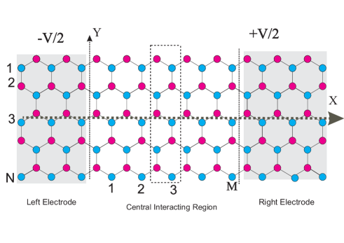
Fig.(1) shows zigzag graphene nanoribbon with an odd number of zigzag chains in width (). Central interacting region, left and right electrodes divide the ribbon into three regions. Odd ZGNRs has a bisection plane which its intersection with the ribbon has been shown as the x-axis in Fig.(1). Although this plane bisects the ribbon, it is not a reflection plane. If upper half of the ribbon is displaced by in respect to the lower one, mirror symmetry is achieved against x-axis. is the bond length of C-C. In other words, part of the wave function which is a functional of variable, is an eigenvector of the parity operator Polini .
III Results
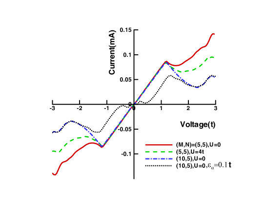
Current-voltage characteristic curve of an odd ZGNR with zigzag chains () is shown in Fig.(2). Lower than the external bias , current increases linearly with the applied bias as an Ohmic device. After a threshold voltage (), NDR occurs at both positive and negative polarity.
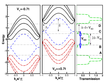
The origin of NDR seen in odd ZGNRs is interpreted by analyzing their energy spectrum accompanied to transmission curve. Fig.(3) shows energy spectrum and transmission through 5-ZGNR at . counts bands from the bottom () to the top of band structure () and is the longitudinal momentum.
In odd ZGNRs, parity has noncommutative relation with the Hamiltonian. Therefore, parity has no conservation and consequently transmission is not blocked by the parity selection rule, while parity conservation in even zigzag nanoribbons opens transmission gap around Fermi levelcheraghchi1 . In the range of of Fig.(3), there exists one conducting channel which results in the unity transmission around the Fermi level. In this range, electrons which occupy states of the lower band of the central band group (the dashed blue bands) belonging to the right electrode are injected into the unoccupied states of the upper band of the central group belonging to the left electrode. So at low biases, current increases linearly with the bias. This single-channel transport around the Fermi level remains unchanged even for high voltages. However, for voltages greater than the NDR threshold voltage (), blocked regions marked by the ranges of and comes into the current integration window. The current integration window, based on Eq. 6 and , is proportional to and is shown with the bold hollow arrows in Fig.(3). Therefore, when the source-drain applied bias increases, current begins to decrease.
Blocked regions ( and ) arise from a selection rule which increases back scattering in the lengthy ribbons. According to this rule, electron transition between those bands which are disconnected from the view point of longitudinal momentum, decreases exponentially with the length. Topology of zigzag graphene ribbons divides the band structure into the three different groupsgrosso . Three groups which are called by upper (n=1,2,3,4), centeral (n=5,6) and lower (n=7,8,9,10) groups, are classified based on the bands which are connected in terms of . Variation of the momentum of electrons passing through the system strongly depends on smoothness or sharpness of the potential. The transition probability of electrons with the state injected by the right electrode into the state as an empty state in the left electrode is proportional to the Fourier transform of the longitudinal voltage grosso as . So smooth variation of the potential in longer ribbons results in a small momentum variation of electron. Consequently, a smooth potential in the longitudinal direction can just scatter electron into those states belonging to the energy bands which are connected from the point of momentum viewgrosso ; cheraghchi1 .
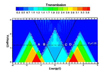
Bias dependent of transmission leads us to plot a contour of transmission in plane of energy and applied bias as shown in Fig.(4). In this figure, the solid lines show the current integration window. Moreover, the dashed lines clarify the regions and corresponding to transport gaps shown in Fig.(3). The intersection of these blocked regions and also the current integration window would be around which is the threshold voltage for the current reduction.
Band structure analyzing demonstrates that the threshold voltage is equal to the half-width of the central bands at as . As shown in Fig.(3), is energy separation of the upper bands from the central bands at the Dirac points. There is a Log-Normal behavior of versus number of zigzag chains () such that as , the NDR threshold voltage asymptotically approaches to the value of . So the NDR threshold voltage slightly decreases with the ribbon width.
Analyzing transport gaps appeared in the band structure shows that they are equal to where . Since approaches to a constant values when , in a given voltage, transport gap is disappeared for which is nearly equivalent to .
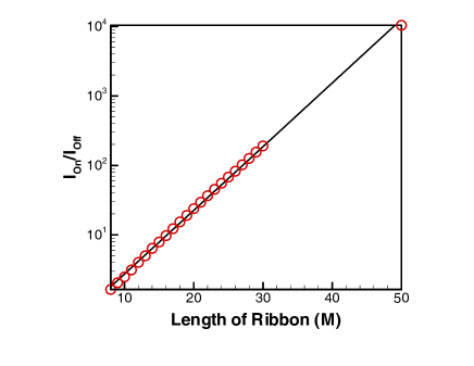
The other effect which enhances performance of this electronic switch, is the ribbon length. Fig.(2) shows an increase of on/off ratio with the ribbon length. Moreover, NDR region () occurs in a more extended range of the I-V curve. Exponential decay of transmission with the length in the gap regions develops quality of switching. It is shown in Fig.(5) that increases exponentially with the ribbon length.
Another parameter which affects I-V curve, is the e-e interaction. In this case, interaction intensifies NDR effects such that off current reduces in compared with non-interacting system and also the region of NDR becomes more extended.
If one of the ribbon edges is doped by small impurity such as , because of a band gap which is induced by edge impurity at the band center, current at low biases decreases. Fig.(2) represents that even with the presence of edge impurity, still the region containing NDR exists. However, asymmetry decreases on/off ratio of the current. Furthermore, asymmetric ZGNR behaves as a semiconductor while symmetric ZGNRs behave as an Ohmic devicesRen . The effect of asymmetry on NDR competes with the ribbon length. Since asymmetry can not be ignored in experiment, longer ribbons are in favor of keeping NDR in the I-V curve.
On the other hand, additional to edge impurity, this asymmetry can be assigned to a sublattice symmetry breaking induced by spontaneous ferromagnetic spin ordering of the electrons localized at the zigzag edgesLouie . In fact, the border atoms at the two opposite zigzag edges belong to different sublattices. So spin orientation along the edges induces different magnetic potentials at the edges. As a result, a small band gap is opened around Fermi level which depending on the ribbon width, is about 0.15 eV. The asymmetry which we have considered is about 0.3 eV which is stronger than the gap opened by spin-polarization of the edges. We can conclude that spin-polarization along the zigzag edges can not affect emerging of this NDR phenomenonRen .
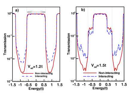
Charging effects: To understand why details of electrostatic potential do not affect the emergence of NDR, we compare transmission in the presence and absence of e-e interaction. Figure (6) compares transmission curves for voltages at the NDR threshold and a larger value such as . It is clear that for voltages lower than the NDR threshold, transmission in the conducting region is robust against e-e interaction. However, for voltages , transmission of conducting region reduces with e-e interaction. This is the reason for reducing off-current in the presence of e-e interaction. Furthermore, transmission curve in the blocked regions and exhibits a little enhancement with the e-e interaction for the whole range of voltages.
To elucidate physics behind to the robustness of NDR phenomenon against e-e interaction, we investigate self-consistent potential profiles which are shown in Fig.(7.a,b). In fact, external potential is well screened by charge redistribution so that potential mostly drops at the contact junctions. This fact is represented in Fig.(7). So, electrostatic potential of atoms located far from contact junctions (deep inside the ribbon) remains nearly flat. In more details, depletion of charge close to the source electrode reduces the source potential as . Therefore, source potential can not penetrate inside the central portion of the system. On the opposite side of system, charge is accumulated close to the drain electrode such that dropping of the potential is weakened.
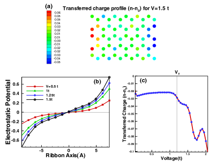
It is useful to investigate bias dependence of total transferred charge from/into the system. Fig.(7.c) shows that transferred charge in compared with its neutrality point value ( with zero source-drain applied bias) decreases for voltages higher than the NDR threshold, while it remains unchanged for voltages . In other words, for , in-flowing and out-flowing charges are balanced with each other, while for , system becomes empty of charge. It can be seen that the threshold voltage for depletion of charge is correlated with the NDR threshold voltage. This behavior is closely similar to what is seen in graphene nano-junctionscheraghchi2 . As a consequence, at high voltages, due to accumulation of charge close to the drain electrode, external potential is always screened in the middle of the graphene strip. Screening effect induces sharp variation of electrostatic potential at the contacts which enhances transition probability between disconnected band groups. Therefore, transmission in the blocked regions ( and ) increases in compared to non-interacting system. However, blocked regions have not any contribution in the current calculation.
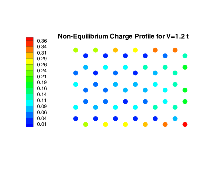
Bottom: Non-equilibrium charge profile at the threshold NDR voltage. Non-equilibrium charge reaches in its maximum value at the ribbon’s edges. Moreover, in agreement with the continuity equation, atomic sites with larger local current corresponds to smaller non-equilibrium charge.
Spatial distribution of bond currents: Charge conservation based on continuity equation yields non-equilibrium bond charge currentnikolic for a non-interacting tight-binding Hamiltonian.
| (8) |
where sites and are nearest-neighbor atoms which their hopping integral is nonzero. Now, charge continuity equation is derived by using Heisenberg equation.
| (9) |
where are the nearest-neighbor atomic site around atomic site. It can be simply proved that the integrands in Equations 3 and 8 are real. In fact, transpose of matrix in Eq.(4) is equal to its conjugate. So, diagonal terms of () and also the terms of () are real.
Bond charge current formulated in Eq.8 has been derived for non-interacting tight-binding Hamiltonian. However, by using Heisenberg equation, it can be simply proved that this formula is still applicable for the Hamiltonian described in Eq.1 in which Hartree interaction appears on diagonal elements of the Hamiltonian. On the other hand, charging effects originating from electrostatic interaction (Hartree term) adjust local currents by means of lesser Green’s function.
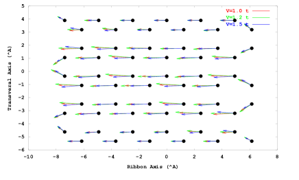
Fig.(8.top) shows spatial profile of local current at each site. In the center of the ribbon, magnitude of local current densities are larger than its value in the zigzag edges of the ribbon. This feature is valid for both ranges of low and high voltages not more than 1.5 t. The reason can be followed by single-channel transport through ZGNR even for high voltagesnikolic . One channel transport is an indirect result of transition rule in which transition between disconnected bands is forbidden. For voltages higher than 1.5 t, alignment of local currents along the ribbon axis is gradually disturbed.
In contrast with the local current distribution, as shown in Fig.(8.bottom), non-equilibrium charge reaches in its maximum value at the ribbon’s edges. This result is compatible with the continuity equation (Eq.9) so that atomic sites with larger local current corresponds to smaller non-equilibrium charge. On the other hand, non-equilibrium charge increases for atomic sites with higher onsite energy due to applied bias (close to the source electrode), while its value tends to zero for sites close to the drain electrode.
Comparison of odd and even ZGNRs: There are some interesting differences between results arising from odd ZGNRs with those results belonging to even ZGNRscheraghchi1 which is kind of odd-even effect. Here, NDR appears in voltages upper than while in even ZGNR, NDR occurs for voltages lower than . On/off ratio of the current in gated even ZGNRs increases as a power law with the function of the ribbon length while here, on/off ratio increases exponentially. Screening of the external bias by electrons of system in even ZGNRs is so stronger than screening effects in odd ZGNRs. As a consequence, the effect of electrostatic interaction on increase of the on/off ratio in even ZGNRs is much effective than in odd ZGNRs. Furthermore, transferred charge from/into the central portion of graphene nanoribbon depends on odd or even zigzag chains in width.
IV Hydrogen Terminated Nanoribbon
To show how passivation of zigzag edges of graphene nanoribbon affects transport properties, we compare the results of the presented model with transport properties calculated by using TranSIESTA codesiesta . This code is based on density functional theory (DFT) approach. We have used the following options to calculate SIESTA code: the generalized gradient approximation (GGA) with the Perdew-Burke-Ernzerhof exchange-correlation functional (PBE)PBE , double- plus polarization orbital (DZP) bases for all atoms, and Troullier-Martins norm conserving pseudopotentials to represent the cores, 200 Ry real space mesh cutoff for charge density and a supercell within 20 of vacuum between the periodic graphene nanoribbons.
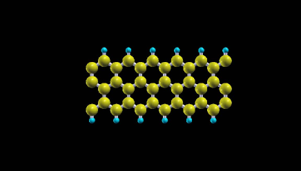
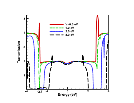
Fig.(9, Top) shows a schematic view of odd zigzag graphene nanoribbon which is saturated by hydrogen atoms. Transmission around the Fermi energy is represented in Fig. (9, bottom). The energy scale is shifted so that the Fermi energy of the system, if there is no bias voltage, is zero (). When there is a finite bias, the Fermi energy of the left electrode is placed at and the right electrode at . The occupation number on atoms in the center part of the system is determined by .
As it is clear of Fig.(9, bottom), there exists one transmitting channel for each spin around Fermi energy level. This result is in complete agreement with the band structure analysis shown in section.III. There exists only one transmitting channel in the region presented in figures 3 and 4. The transport gap in Fig. (9, bottom) begins to open at voltage around and for energy about . These points correspond to the points marked by cross sign in Fig.4 in which the transport gap begins to open as the applied bias increases. As a result, we demonstrate that the transport gap which is responsible for emerging the NDR phenomena could also be opened in graphene nanoribbons with passivated zigzag edges.
V Conclusion
As a conclusion, based on a model calculation of non-equilibrium Green’s function formalism, we found that there exists a region of negative differential resistance in I-V curve of ultra narrow (lower than ) zigzag graphene nanoribbons with odd number of zigzag chains in width. This NDR is induced by a transport gap which originates from electronic transition between disconnecting bands of energy from the view point of longitudinal momentum. On/off ratio of the current exponentially increases up to as a function the ribbon length which proposes possibility of manipulation of odd ZGNRs as high quality switch in nanoelectronic based on graphene nanoribbons. In addition, e-e interaction enhances on-off ratio of the current which originates from a flat electrostatic potential deep inside the ribbon due to screening of the external bias by electrons close to the junctions. By using continuity equation, spatial profile of local currents is calculated in the presence of Hartree electron interactions. In both high and low biases, local current reaches to its maximum values in the center of the ribbon while in contrast with the local current profile, non-equilibrium charge has its maximum values at the edges of the ribbon. Furthermore, this NDR is not much sensitive to the edge asymmetry. So emerging of this NDR is robust against spin orientation along the edges.
By using ab initio density functional theory, we also show that the transport gap which is responsible for emerging NDR, exits in passivated graphene nanoribbons by Hydrogen atoms.
References
- (1) K. S. Novoselov, et al., Science 306, 666 (2004).
- (2) Z. Liu, et al., Phys. Rev. Lett. 102, 015501 (2009). B. Ozyilmaz, et al., Phys. Rev. Lett. 99, 166804 (2007). M. Y. Han,et al., Phys. Rev. Lett. 98, 206805 (2007).
- (3) X. Li, X. Wang, L. Zhang, S. Lee, H. Dai, Science, 319, 1229 (2008); X. Wang, Y. Ouyang, X. Li, H. Wang, J. Guo, H. Dai, Phys. Rev. Lett. 100, 206803 (2008).
- (4) M. Y. Han, B. ozyilmaz, Y. Zhang, and P. Kim, Phys. Rev. Lett. 98, 206805 (2007); F. Molitor, A. Jacobsen, C. Stampfer, J. G ttinger, T. Ihn, and K. Ensslin, Phys. Rev. B. 79, 075426 (2009).
- (5) F. Molitor, A. Jacobsen, C. Stampfer, J. G ttinger, T. Ihn, and K. Ensslin, Phys. Rev. B. 79, 075426 (2009).
- (6) A. Cresti, G. Grosso, G. P. Parravicini, Phys. Rev. B. 78, 115433 (2008); Phys. Rev. B. 77, 233402 (2008).
- (7) A. R. Akhmerov, J. H. Bardarson, A. Rycerz, and C. W. J. Beenakker, Phys. Rev. B. 77, 205416 (2008).
- (8) Z. Li, H. Qian, J. Wu, B. L. Gu, W. Duan, Phys. Rev. Lett. 100, 206802 (2008).
- (9) Z. F. Wang, et al., Appl. Phys. Lett. 92, 133114(2008).
- (10) J. Nakabayashi, D. Yamamoto, and S. Kurihara, Phys. Rev. Lett. 102, 066803 (2009).
- (11) K. Wakabayashi and T. Aoki, Int. J. Mod. Phys. B. 16,4897 (2002).
- (12) H. Cheraghchi, H. Esmailzadeh, Nanotechnology, 21, 205306 (2010).
- (13) L. Esaki, Phys. Rev. 109, 603 (1958)
- (14) A.A. Farajian, K. Esfarjani and Y. Kawazoe, Phys. Rev. Lett. 82, 5084 (1999).
- (15) D. Dragoman, M. Dragoman, Appl. Phys. Lett. 90, 143111 (2007).
- (16) Y. Kobayashi, et al., Phys. Rev. B. 73, 125415 (2006); Y. Niimi, et al., Phys. Rev. B. 73, 085421 (2006).
- (17) H. Cheraghchi, K. Esfarjani, Phys. Rev. B. 78, 085123 (2008), see also its references.
- (18) J. Taylor, H. Guo, J. Wang, Phys. Rev. B. 63, 245407 (2001).
- (19) S.Datta, Electronic Transport in Mesoscopic Systems (Cambridge U.P, Cambridge, 1995).see chapter 2 and references.
- (20) M. C. Munoz, et al., Prog. Surf. Sci. 26, 117 (1988); F. Garcia-Moliner and V. R. Velasco, Theory of Single and Multiple interfaces (World Scientific, Singapore, 1992).
- (21) D. Rainis, F. Taddei, F. Dolcini, M. Polini, R. Fazio, Phys. Rev. B. 79, 115131 (2009).
- (22) Y. W. Son, M. L. Cohen, and S. G. Louie, Phys. Rev. Lett. 97, 216803 (2006).
- (23) Y. Ren and K-Q. Chen, J. Appl. Phys, 107, 044514 (2010).
- (24) B. K. Nikolic, P. L. Zarbo and S.Souma, Phys. Rev. B. 73, 075303 (2006); L. P. Zarbo and B. K. Nikolic, Europhys. Lett. 80 47001 (2007).
- (25) J. M. Soler, et al, Journal of Physics: Condensed Matter, 14, 2745 (2002).
- (26) J. P. Perdew, K. Burke, and M. Ernzerhof, Phys. Rev. Lett. 77, 3865 (1996).