A perfect absorber made of a graphene micro-ribbon metamaterial
Abstract
Metamaterial-based perfect absorbers promise many applications. Perfect absorption is characterized by the complete suppression of transmission and reflection and complete dissipation of the incident energy by the absorptive meta-atoms. A certain absorption spectrum is usually assigned to a bulk medium and serves as a signature of the respective material. Here we show how to use graphene flakes as building blocks for perfect absorbers. Then, an absorbing meta-atom only consists of a molecular monolayer placed at an appropriate distance from a metallic ground plate. We show that the functionality of such device is intuitively and correctly explained by a Fabry-Perot model.
Institute of Condensed Matter Theory and Solid State Optics, Abbe Center of Photonics, Friedrich-Schiller-Universität Jena, Max-Wien-Platz 1, D-07743 Jena, Germany \email∗Rasoul.Alaee@uni-jena.de
(050.6624) Subwavelength structures;(160.3918) Metamaterials; (310.3915) Metallic, opaque, and absorbing coatings.
References
- [1] H. P. Boehm, A. Clauss, G. O. Fischer, and U. Hofmann, “Dünnste kohlenstoff-folien,” Z. Naturforschg. 17, 150–157 (1962).
- [2] K. S. Novoselov, A. K. Geim, S. V. Morozov, D. Jiang, Y. Zhang, S. V. Dubonos, I. V. Grigorieva, and A. A. Firsov, “Electric field effect in atomically thin carbon films,” Science 306, 666–669 (2004).
- [3] A. H. Castro Neto, F. Guinea, N. M. R. Peres, K. S. Novoselov, and A. K. Geim, “The electronic properties of graphene,” Rev. Mod. Phys. 81, 109–162 (2009).
- [4] S. Stankovich, D. A. Dikin, G. H. B. Dommett, K. M. Kohlhaas, E. J. Zimney, E. A. Stach, R. D. Piner, S. T. Nguyen, and R. S. Ruoff, “Graphene-based composite materials,” Nature 442, 282–286 (2006).
- [5] C. Berger, Z. Song, X. Li, X. Wu, N. Brown, C. Naud, D. Mayou, T. Li, J. Hass, A. N. Marchenkov, E. H. Conrad, P. N. First, and W. A. de Heer, “Electronic confinement and coherence in patterned epitaxial graphene,” Science 312, 1191–1196 (2006).
- [6] R. R. Nair, P. Blake, A. N. Grigorenko, K. S. Novoselov, T. J. Booth, T. Stauber, N. M. R. Peres, and A. K. Geim, “Fine structure constant defines visual transparency of graphene,” Science 320, 1308 (2008).
- [7] M. Liu, X. Yin, E. Ulin-Avila, B. Geng, T. Zentgraf, L. Ju, F. Wang, and X. Zhang, “A graphene-based broadband optical modulator,” Nature 474, 64–67 (2011).
- [8] A. Vakil, and N. Engheta, “Transformation optics using graphene,” Science 332, 1291–1294 (2011).
- [9] P.-Y. Chen, and A. Alù, “Atomically-thin surface cloak using graphene monolayers,” ACS Nano 5, 5855–5863 (2011).
- [10] J. Christensen, A. Manjavacas, S. Thongrattanasiri, F. H. L. Koppens, and F. J. G. de Abajo, “Graphene plasmon waveguiding and hybridization in individual and paired nanoribbons,” ACS Nano 6, 431–440 (2012).
- [11] A. Manjavacas, P. Nordlander, and F. J. G. de Abajo, “Plasmon blockade in nanostructured graphene,” ACS Nano 6, 1724–1731 (2012).
- [12] L. Ju, B. Geng, J. Horng, C. Girit, M. Martin, Z. Hao, H. A. Bechtel, X. Liang, A. Zettl, Y. R. Shen, and F. Wang, “Graphene plasmonics for tunable terahertz metamaterials,” Nat. Nanotechnology 6, 630–634 (2011).
- [13] Z. Fei, A. S. Rodin, G. O. Andreev, W. Bao, A. S. McLeod, M. Wagner, L. M. Zhang, Z. Zhao, M. Thiemens, G. Dominguez, M. M. Fogler, A. H. Castro Neto, C. N. Lau, F. Keilmann and D. N. Basov, “Gate-tuning of graphene plasmons revealed by infrared nano-imaging,” Nature 487, 82–85 (2012).
- [14] J. Chen, M. Badioli, P. Alonso-Gonz lez, S. Thongrattanasiri, F. Huth, J. Osmond, M. Spasenovic, A. Centeno, A. Pesquera, P. Godignon, A. Z. Elorza, N. Camara, F. J. G. de Abajo, R. Hillenbrand and F. H. L. Koppens, “Optical nano-imaging of gate-tunable graphene plasmons,” Nature 487, 77–81 (2012).
- [15] E. H. Hwang, and S. Das Sarma, “Dielectric function, screening, and plasmons in two-dimensional graphene,” Phys. Rev. B 75, 205418 (2007).
- [16] F. Rana, “Graphene terahertz plasmon oscillators,” IEEE Trans. Nanotechnol 7, 91-99 (2008).
- [17] M. Jablan, H. Buljan, and M. Soljacic, “Plasmonics in graphene at infrared frequencies,” Phys. Rev. B 80, 245435 (2009).
- [18] A. Yu. Nikitin, F. Guinea, F. J. Garcia-Vidal, and L. Martin-Moreno, “Fields radiated by a nanoemitter in a graphene sheet,” Phys. Rev. B 84, 195446 (2011).
- [19] P.Tassin, T. Koschny, M. Kafesaki and C. M. Soukoulis, “A comparison of graphene, superconductors and metals as conductors for metamaterials and plasmonics,” Nature Photonics 6, 259–264 (2011).
- [20] F. H. L. Koppens, D. E. Chang, and F. J. G. de Abajo, “Graphene plasmonics: a platform for strong light-matter interactions,” Nano Lett. 11, 3370–3377 (2011).
- [21] N. I. Landy, S. Sajuyigbe, J. J. Mock, D. R. Smith, and W. J. Padilla, “Perfect metamaterial absorber,” Phys. Rev. Lett. 100, 207402 (2008).
- [22] C. M. Watts, X. Liu, and W. J. Padilla, “Metamaterial electromagnetic wave absorbers,” Adv. Mater. 24, OP98–OP120, (2012).
- [23] T. V. Teperik, F. J. G. de Abajo, A. G. Borisov, M. Abdelsalam, P. N. Bartlett, Y. Sugawara, and J. J. Baumberg, “Omnidirectional absorption in nanostructured metal surfaces,” Nat. Photonics 2, 299 -301 (2008).
- [24] Y. Avitzour, Y. A. Urzhumov, and G. Shvets, “Wide-angle infrared absorber based on a negative-index plasmonic metamaterial,” Phys. Rev. B 79, 045131 (2009).
- [25] K. Aydin, V. E. Ferry, R. M. Briggs, and H. A. Atwater, “Broadband polarization-independent resonant light absorption using ultrathin plasmonic super absorbers,” Nat. Commun. 2, 517 (2011).
- [26] X. Liu, T. Tyler, T. Starr, A. F. Starr, N. M. Jokerst, and W. J. Padilla, “Taming the blackbody with infrared metamaterials as selective thermal emitters,” Phys. Rev. Lett. 107, 045901 (2011).
- [27] N. Liu, M. Mesch, T. Weiss, M. Hentschel and H. Giessen, “Infrared perfect absorber and its application as plasmonic sensor,” Nano Lett. 10, 2342–2348 (2010).
- [28] C. Wu, and G. Shvets, “Design of metamaterial surfaces with broad-band absorbance,” Opt. Lett. 37, 308–310 (2012).
- [29] C. Wu, B. Neuner, G. Shvets, J. John, A. Milder, B. Zollars, and S. Savoy, “Large-area wide-angle spectrally selective plasmonic absorber,” Phys. Rev. B 84, 075102 (2011).
- [30] Y. D. Chong, Li Ge, Hui Cao, and A. D. Stone, “Coherent perfect absorbers: time-reversed lasers,” Phys. Rev. Lett. 105, 053901 (2010).
- [31] W. Wan, Y. Chong, L. Ge, H. Noh, A. D. Stone, and H. Cao, “Time-reversed lasing and interferometric control of absorption,” Science 331, 889–892 (2011).
- [32] S. Thongrattanasiri, F. H. L. Koppens, and F. J. G. de Abajo, “Complete optical absorption in periodically patterned graphene,” Phys. Rev. Lett. 108, 047401 (2012).
- [33] A. Yu. Nikitin, F. Guinea, F. J. Garcia-Vidal, and L. Martin-Moreno, “Surface plasmon enhanced absorption and suppressed transmission in periodic arrays of graphene ribbons,” Phys. Rev. B 85, 081405(R) (2012).
- [34] C. Wu, B. Neuner, G. Shvets, J. John, A. Milder, B. Zollars, and S. Savoy, “Large-area wide-angle spectrally selective plasmonic absorber,” Phys. Rev. B 84, 075102 (2011).
- [35] W. W. Salisbury, “Absorbent body for electromagnetic waves,” US Patent 2599944 (1952).
- [36] H. T. Chen, “Interference theory of metamaterial perfect absorbers,” Opt. Express 20, 7165–7172 (2012).
- [37] L. Huang, D. R. Chowdhury, S. Ramani, M. T. Reiten, S.-N. Luo, A. K. Azad, A. J. Taylor, and H. T. Chen, “Impact of resonator geometry and its coupling with ground plane on ultrathin metamaterial perfect absorbers,” Appl. Phys. Lett. 101, 101102 (2012).
- [38] P. Yeh, “Optical waves in layered media” Wiley, New York, (2005).
- [39] G. W. Hanson, “Dyadic Green s functions and guided surface waves on graphene,” J. Appl. Phys. 103, 064302 (2006).
- [40] L. A. Falkovsky, S. S. Pershoguba, “Optical Far-Infrared Properties of a Graphene Monolayer and Multilayer,” Phys. Rev. B 76, 153410 (2007).
- [41] E. H. Hwang and S. Das Sarma “Dielectric function, screening, and plasmons in two-dimensional graphene,” Phys. Rev. B 75, 205418 (2007).
- [42] V. P. Gusynin, S. G. Sharapov and J. P. Carbotte “Magneto-optical Conductivity in Graphene,” J. Phys. Condens. Matter, 19, 026222 (2007).
- [43] L. Li, “New formulation of the fourier modal method for crossed surface-relief gratings,” J. Opt. Soc. Am. A 14, 2758–2767 (1997).
1 Introduction
Graphene is a two-dimensional (2D) carbon material with tremendous applications. In 1962 it was isolated by Boehm et al. for the first time [1]. More recently, in 2004, a team led by Geim proposed a more efficient way to produce it based on exfoliation procedures. That moment was the starting point for the rise of graphene [2]. The research was fueled by the extraordinary electronic transport properties of graphene which differ substantially from those in metals and semiconductors [3]. In fact, electrons behave like massless particles when they propagate in graphene sheets, like photons do in matter with the notable difference that they have an electric charge. These unprecedented electronic properties make graphene a serious candidate for the material of the century [4, 5] to be used for ultrafast, low loss electronic devices because of its high conductivity and its extraordinary mechanical parameters.
Likewise the optical properties of graphene attracted a great deal of research interest. In the visible, graphene acts as an absorptive dielectric. The absorption A of a single sheet amounts to [6, 3], with being the fine structure constant. Various applications, ranging from graphene based optical modulators [7], transformation optics [8] to numerous other devices [9, 10, 11] may be envisaged by using graphene in the optical domain. Examples have been already experimentally demonstrated and have been provided solid evidence for the versatility of graphene [12, 13, 14].
At lower frequencies, the optical properties of graphene resemble those of a Drude-type material. Such materials promote the formation of surface plasmon polaritons (SPP). An SPP is a collective oscillation of the charge density and light at the interface between a graphene sheet and its surrounding [13, 14, 15, 16, 17, 18]. An SPP supported at a graphene interface can be guided in many ways like other types of waves (light or sound). This property attracted a particular interest of the metamaterial and plasmonic community [20, 19].
One of the most interesting properties of plasmonic metamaterials is the perfect absorption of light [21, 22]. Such functionality was demonstrated while relying on different designs and while optimizing the point of operation over large frequency ranges [23, 24, 25, 26, 27, 28, 29]. The functionality of such perfect absorbers can be understood in the framework of the more general theory of coherent perfect absorption (CPA). It is in many ways the time-reversed analogue of the lasing effect. Instead of radiating a coherent flux of light in a very narrow spectral band [30, 31], CPA can occur for structures possessing intrinsic losses. It only requires that an incoming radiation pattern is dissipated by suppressing the associated reflection and transmission channels. In fact, the CPA effect can only occur because of the interplay of interference and absorption being achievable just for a very specific geometry and frequency range. More recently, graphene nanodisks were suggested for this purpose [32]. It was shown that graphene flakes allow for the perfect absorption of THz radiation owing to their high extinction cross section (compared to their geometrical cross section). Such perfect absorption has also been achieved when the discs were put in front of a mirror at some distance.
Recently graphene micro-ribbons is theoretically and experimentally studied [33, 12]. In this paper we propose to take advantage of the recent technological progress in fabricating nanostructured graphene layers grown on dielectric substrates [12]. We show that perfect absorption can be achieved by patterned graphene micro-ribbons on a thick dielectric layer deposited on top of a reflecting metal substrate. Furthermore, we show that the complete light absorption is almost independent of angle of incidence and its frequency can be easily tuned by changing the chemical potential or gate voltage.
The modus operandi of the suggested perfect absorber differs from that of the ordinary ones made of metallic nanoparticles brought in close proximity to a metallic ground plate. There, the current induced in the ground plate via a near-field interaction is out-of-phase to the current in the nanoparticle. This causes the resonance to be dark and radiative losses to be reduced. If the condition of critical coupling is achieved, the incident light can be fully absorbed [34]. In striking contrast, the device we suggest and study here is characterized by a thick dielectric intermediate layer that prohibits any near-field interaction between the nanostructured graphene and the ground plate. This type of perfect absorber is known as the Salisbury screen or absorber [35]. Instead, perfect absorption is achieved by exploiting a perfect destructive interference of the reflected light [22, 35, 36, 37]. Transmission through the structure is totally suppressed because the thickness of the ground plate is much larger than the typical skin depth at THz frequency. Therefore, the complete electromagnetic energy gets absorbed by the graphene micro-ribbons. We explain our findings by considering the micro-ribbons as a metasurface. This allowed us to describe them only by their reflection and transmission coefficients and using Airy formula for an asymmetric Fabry Perot cavity to calculate the absorption in the device [38]. Predictions from such simple model are in excellent agreement with full-wave simulations and clearly prove that the perfect absorption is a purely coherent effect.
2 Graphene perfect absorber
The structure under consideration is shown in Fig. 1. It consists of a graphene micro-ribbon array on top of a metallic ground plate separated by a thick dielectric spacer. It is periodic in one direction () with periodicity m and infinitely extended in the other one. We assume the refractive index () of the dielectric deposited on the metal. The ground plate is made of gold with a conductivity S/m which is perfectly reflecting in the frequency domain of interest (Far-infrared regime).
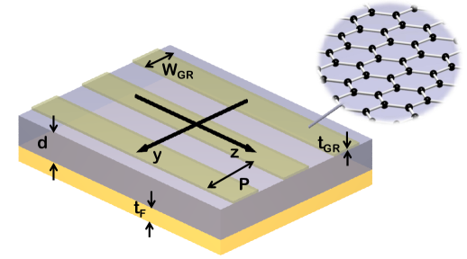
The graphene was numerically modeled by a thin layer ( with thickness nm) of permittivity , with as the surface conductivity of the graphene sheet [8] which can be derived using the well-known Kubo formula [39, 40, 41, 42] and writes as:
| (1) |
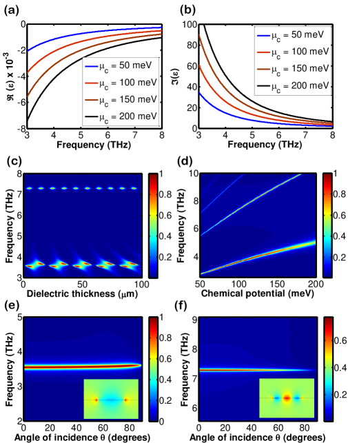
where , and are universal constants related to the electron charge, Planck’s and Boltzmann’s constant, respectively. is the temperature and is fixed to 300 K. and (, is the electron-phonon relaxation time) are physical parameters of the graphene sheet and account for the chemical potential (or Fermi energy) and the intrinsic losses, respectively. We assumed meV in this contribution and this value is based on the theoretical estimation of maximum mobility in graphene [39]. Furthermore, it should be noted that even for a larger scattering rate the general functionality of proposed device is not affected and all the phenomena can be observed. The frequency of operation is in the Far-infrared regime (1-10 THz). The parameter was taken 1 nm in our study, and the convergence of was verified numerically (by taking the limit ) and by reproducing some previous results [20, 12, 32]. In addition, the frequency dependent permittivity of graphene depending on the some selected values of the chemical potential are shown in Fig. 2(a) and 2(b).
The geometrical parameters of our structure are selected based on experimental capabilities [12], a filling fraction was shown to be easier for fabrication (see Fig. 1). Nevertheless, the very parameters are of marginal importance and variations would only cause a slight modification of the frequency of operation. The set-up is illuminated by a transverse magnetic (TM) incident plane wave. The Fourier Modal Method (FMM) is used to explore the underlying physics of the absorber [43]. The method solves Maxwell’s equations for the periodic structure rigorously. In order to have convergent results, 101 Fourier orders were selected in all numerical results presented herein.
Figure 2(c) shows the absorption A of the graphene micro-ribbons (of Fig. 1) as function of the thickness of the spacer and the frequency of operation. The strong coupling of the Fabry-Perot resonance with the localized eigenmode of the graphene micro-ribbons is clearly visible in Fig. 2(c) and this leads to an avoided crossing and a significant Rabbi splitting. The results reveal that perfect absorption () can be achieved at various values of , periodically spaced between 1 and 100 m around a frequency of 3.6 THz for the first mode (dipolar one) and around 7.3 THz for the second mode, where the peaks are less pronounced (). However, by optimizing the geometry and tuning the chemical potential, we have verified that it is possible to achieve total absorption for both modes (this is not included in this contribution). Moreover, the resonance frequency of maximum absorption is slightly changing for different dielectric spacer and this effect is more pronounced for the first mode (see Fig. 2(c)). In Fig. 2(d) the absorption as a function of the chemical potential (ranging from 50 to 200 meV) and the frequency is displayed. It can be clearly seen that the resonance frequency of the absorber can be tuned over a wide range by varying . It should be mentioned that by applying a gate voltage (a static electric field) or by means of chemical doping, the chemical potential and thus the conductivity of graphene can be controlled on purpose.
In order to investigate the robustness of the graphene perfect absorber, the absorption as a function of frequency and the angle of incidence is displayed in Fig. 2(e) and 2(f). The first mode is almost unaffected while varying the angle of incidence until 80 degrees [Fig. 2(e)]. Then absorption starts to decrease. The behavior of the higher order mode (the second mode for instance) is quite different, as shown in Fig. 2(f), where the absorption is strongly dependent on the angle of incidence and significantly decreases beyond 50 degrees to vanish completely at about 80 degrees. The electric field distribution (component parallel to the gap) at plasmon resonance is displayed for both modes in the insets of Fig. 2(e) and 2(f), respectively, and confirms the nature of the excited modes [dipole and higher order].
3 Mechanism of complete absorption
Let us focus now on the underlying mechanism of perfect absorption for graphene. To simplify the structure and to provide a physical explanation, we shall consider the structure as an asymmetric Fabry-Perot cavity with two mirrors, i.e., a graphene micro-ribbon array as the top mirror and the metallic ground plate as the bottom mirror. The transmission channel () of the system is completely suppressed by choosing a sufficiently thick ground plate (). In order to achieve total absorption of the incident energy () the reflection channel must be closed as well () which is the sum of the direct reflection coefficient and the multiple reflection coefficient [as sketched in Fig. 3(e)]. The total reflection coefficient can be expressed as [38]:
| (2) |
where, , , , , are complex-valued transmission and reflection coefficients at both interfaces, is the phase accumulated upon a cavity transfer, is the free space wavenumber, is the refractive index of the dielectric, and is its thickness.
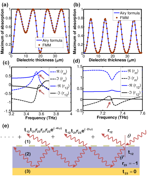
The dependence of the absorption maxima on the dielectric spacer thickness calculated by using the Airy formula (Eq. 2) is shown in Fig. 3 for the first (a) and the second (b) modes. This formula could be used by considering the graphene micro-ribbons as a metasurface (this could be justified by its extremely small thickness compared to other dimensions and to the wavelength), and it is completely defined by its reflection and transmission coefficients. These coefficients were calculated using FMM while assuming that the sufficient thin graphene metasurface is sandwiched between two semi-infinite half-spaces; one of them being air; the other being the dielectric. Assuming an excitation with a linearly polarized incident plane wave either from the top medium (air) or from the bottom medium (dielectric), provides unambiguously the coefficients , , , and , respectively.
For comparison, the rigorous calculations (using FMM) are also
displayed in the same figure, and a perfect agreement between
the two methods is evident for both modes [see
Fig. 3(a) and 3(b)]. In
addition, the real and imaginary parts of the multiple
reflection coefficient and the direct reflection
coefficient are plotted in Fig. 3(c)
and 3(d) again for both modes. Let us
concentrate for a while on the first mode [Fig.
3(c)]; at the resonance frequency
THz, and for a spacer thickness m, both coefficients
and have the same phase and opposite
amplitude. Hence, the resulting total reflection coefficient is
completely canceled due to destructive interference (). As a result, the absorption is almost unity for this
frequency. However, we expect for the second mode, resonant at
THz that the multiple reflection coefficient can not
totally eliminate the direct reflection coefficient at
m because the absorption is less than unity,
[see Fig. 3(d)]. But as mentioned
earlier, this issue could be fixed by optimizing the structure
which is beyond the scope of this paper.
4 Conclusion
To conclude, in this contribution we have discussed a new
class of perfect absorbers in the Far-infrared regime based on
graphene micro-ribbons. Our structure showed complete
absorption for the first mode and for different geometrical
configurations. The robustness of the mechanism was evidenced
by analyzing its dependence on the angle of incidence and the
chemical potential of the graphene sheets. Moreover, we
utilized a semi-analytical approach based on a Fabry-Perot
model that explains very well the observed behavior. We believe
that our study demonstrates the versatility of graphene and
could be used in future for optical or THz interconnects.
Acknowledgments
This work was partially supported by the German Federal Ministry of Education and Research (Metamat and PhoNa) and by the Thuringian State Government (MeMa).