Cyclic Depopulation of Edge States in a large Quantum Dot
Abstract
We investigate magneto-transport through a 1.6 m wide quantum dot (QD) with adjacent charge detector, for different integer filling factors in the QD and constrictions. When this system is operated at a high transmission, it acts as a Fabry-Pérot interferometer, where transport is governed by a Coulomb blockade mechanism. For lower transmissions where the barriers are in the tunneling regime, we can directly measure the charge stability diagram of two capacitively and tunnel coupled Landau levels. The tunneling regime has been investigated in direct transport, as well as in single electron counting. The edge states within the dot are non-cyclically depopulated, which can be explained by a simple capacitive model and allows to draw conclusions about the edge state geometry within the quantum dot.
pacs:
73.43.Lp, 72.20.-i, 72.25.Dc, 73.23.Hk, 81.07.Ta1 Introduction
Two-dimensional electron systems at low temperatures and in strong magnetic fields show a rich spectrum of highly degenerate, incompressible ground states [1, 2]. Fractional quantum Hall states, occurring at a fractional filling factor with an odd denominator, are well described by the Laughlin wavefunction [3]. There exists a prominent exception from this hierarchy: the state [4], which is believed to obey non-abelian statistics [5, 6]. This remarkable property could make it an interesting candidate for the realization of a topological qubit [7]. Theoretical ideas for probing the statistics of the state are based on quantum dots, operated as Fabry-Pérot interferometers as a basic building block [8, 9, 10, 11, 12].
Quantum dots exposed to a magnetic field also offer other interesting fields of study, as the investigation of the spin configuration [13] or few-electron addition spectra [14]. In the presence of a strong magnetic field, Coulomb blockade (CB) oscillations can no longer be described within a single-particle picture. Alternating compressible and incompressible regions are formed inside the dot, which can strongly modify the CB oscillations [15]. Previous experiments have allowed the extraction of mutual capacitances of these regions for different filling factors [16]. In those experiments, alternating high and low CB peak currents have been observed, which was attributed to a double dot-like behavior of two edge states inside the dot. However, for the interpretation of recent experiments using quantum dots as Fabry-Pérot interferometers [17, 18, 19], it is important to understand the detailed structure of edge states inside the QD and the parameter range, where this description is valid.
Here we present investigations of a large quantum dot with a quantum point contact (QPC) serving as a charge detector. When the QD is operated as a Fabry-Pérot interferometer, we find resonances with a slope in voltage - magnetic field space and a periodicity characteristic for a Coulomb dominated effect, as already observed in previous experiments [17, 18, 19].
When the system is operated at a lower transmission where the barriers are in the tunneling regime, we observe a similar effect as in Ref. [16]. However, the amplitude modulation can be observed over a large parameter range for different filling factors, allowing the direct measurement of the charge stability diagram of capacitively and tunnel coupled edge states. As a consequence, we can estimate the width of the incompressible region separating the edge channels inside the QD. In contrast to previous experiments, this is accomplished by using capacitances, directly extracted from the measured charge stability diagram. Furthermore we are able to investigate the CB amplitude modulation by using (time-resolved) charge detection techniques, where it shows up as an increased / decreased tunneling rate. To our knowledge, single electron counting has never been performed with a QD of similar size. Direct transport measurements do not always reflect the full complexity of the edge state substructure inside a QD. In future experiments, single electron counting might provide additional important insight to charge localization and transport in micron-sized Fabry-Pérot interferometers.
Most proposed Fabry-Pérot interferometry experiments for probing properties of fractional quantum Hall states assume edge states to be one-dimensional electron or composite fermion channels with negligible interaction between compressible regions. We show, that when the edge states are confined to the QD, a complex behavior with compressible and incompressible regions is observed. The observed tunnel-coupling between the different compressible regions, i.e. the presence of tunnel-coupled alternative paths, might influence the outcomes of the proposed interferometry experiments.
2 Experimental details
The quantum dot has been fabricated on a Hall-bar, defined by wet-etching of a single-side doped GaAs/AlxGa1-xAs heterostructure with a mobility of and an electron density of . These structures employ a reduced proportion of Al in the spacer layer between the doping plane and the 2DEG (x=0.24 compared to x=0.30 or x=0.33 which are most widely used), which was shown to favor the formation of the state [20]. The electron gas resides 340 nm below the surface. Optical lithography, combined with chemical etching and metal evaporation are used to define the mesa, ohmic contacts and topgate leads. The quantum dot and charge detector gates are defined by electron-beam lithography with subsequent metal evaporation. Applying a negative voltage of to the topgates depletes the electron gas underneath. Compared to double-side doped quantum wells with -doped screening layers, this structure allows for a much better gateability [21]: the conductance of a single QPC is non-hysteretic and stable in time. Measurements have been conducted in a dry dilution refrigerator at a base temperature of 10 mK and in magnetic fields between B = 0 T and B = 5 T, using standard four-terminal lock-in measurement techniques. A constant AC voltage modulation of an amplitude has been applied via a current-to-voltage converter.
3 Results and discussion
3.1 Zero magnetic field transport
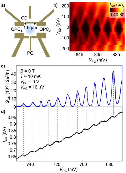
Fig. 1a shows the topgate layout of the quantum dot that has been used for the measurements. The two 800 nm wide QPCs with a channel length of 600 nm serve as tunnel barriers of the 1.6 m wide quantum dot. The employed QPCs have shown to result in an almost harmonic confinement potential, apart from the regime very close to pinch-off [21]. The special geometry ensures a smooth QPC potential which is believed to favor the self-consistent formation of separated edge states.
In addition to the plunger gate (PG) that allows for the tuning of the electrochemical potential of the QD, a QPC that serves as a charge detector (CD) [22, 23] has been implemented. When QPC1 and QPC2 are in the tunneling regime, finite-bias measurements give rise to characteristic Coulomb diamonds (Fig 1b), from which we extract charging energies of about 100 eV. The Coulomb diamond measurement also demonstrates the good stability and control of the QD. Sharp kinks in the CD current (Fig. 1d), aligned with peaks in the dot conductance indicate addition / depletion of a single electron from the quantum dot. By pinching off the tunnel barriers even more, time-resolved single electron counting [24, 25, 23] is possible for rates below approx. 50 Hz.
3.2 Non-cyclic depopulation of edge channels
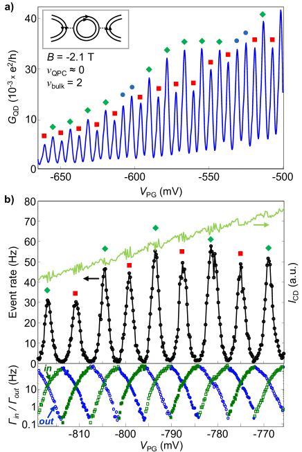
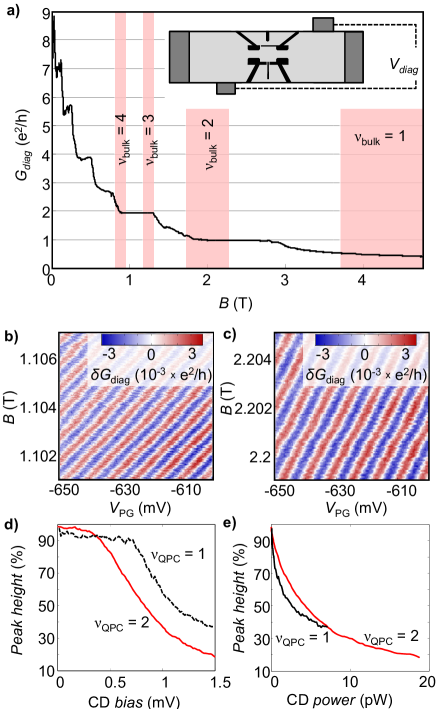
For a bulk filling factor of , a filling factor in the quantum dot of and , i.e. when two spin-split edge states that are formed in the bulk, as well as in the dot are tunnel-coupled across the QPCs (see schematic inset Fig. 2a), CB oscillations are distinctly different from zero magnetic field measurements: the peak height of adjacent CB peaks alternates between two different values (Fig. 2a). After five peaks of high amplitude (marked by diamonds) and 6 peaks of low amplitude (squares), two peaks of similar height (filled circles) appear. The alternating peak height can also be seen in the single electron counting regime (Fig. 2b). Here, the rate of tunnelling events between dot, source and drain (black line, extracted from a time-resolved measurement of the charge detector current) is plotted as a function of the plunger gate voltage . The contrast between peaks of high and low amplitude is lower than in the direct transport measurements. However, taking into account the amplitude dependence on the the plunger gate voltage (decreased Coulomb peak height as is decreased), we still have a peak height difference of roughly 15%, bigger than our detection error. Tunneling-in () and tunneling-out () rates have been extracted from time-resolved measurements of the charge detector conductance. Apart from the different event rate at the Coulomb peak maxima, no further evidence of additional levels contributing to transport or more complex processes, like electron bunching [26], could be found. As argued later, this means that tunneling processes within the dot are much faster than processes between the quantum dot and the leads.
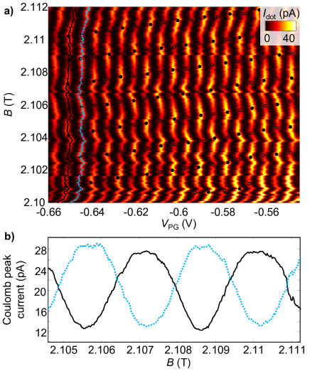
Measuring the CB oscillations as a function of PG voltage and magnetic field, a complex pattern of peak maxima is found (Fig. 3a). By extracting the peak amplitude minima (empty circles) and maxima (filled circles) numerically, it can be seen that they are distributed according to a tilted chessboard pattern, as indicated by the filled and empty circles in Fig. 3a. Along a Coulomb peak (black or blue (grey) line in Fig. 3a,b), the peak current is modulated as a function of the magnetic field (Fig. 3b). Neighboring Coulomb peaks show opposite amplitude dependencies.
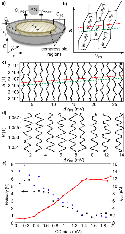
Dominant shifts and drifts of the CB peaks in the measurement of Fig. 3a, make it impossible to investigate the absolute position of the peaks. However, modulations in the voltage spacing of two adjacent peaks can clearly be observed (Fig. 4c). Here, we plot of two successive CB peaks, offset in x-direction for better visibility. Similar measurements can be conducted for a bulk filling factor . In this case, bulk transport measurements suggest two spin-degenerate edge states separated by an incompressible region. Fig. 4d shows the voltage distance between adjacent CB peaks for this case.
The described behavior can be explained by a capacitive model [16]: at a filling factor of in the quantum dot, the edge states corresponding to the spin-split lowest Landau level (LL) form compressible regions inside the quantum dot. We denote the lower / upper spin-split part of the lowest Landau level by LL1 and LL2. The width of these regions is dictated by self-consistency of the edge potential and the electrostatic potential contribution of the electron density [27]. In-between the compressible rings (shown schematically in Fig. 4a as thick lines), an incompressible region with a magnetic field dependent width is formed (hatched region). In this situation, electrons in both Landau levels populate the whole disk-shaped area in the quantum dot. However, only the compressible regions contribute to electron transport. Both spin-split levels inside the dot are tunnel coupled to source and drain and capacitively coupled to the plunger gate, as well as to the leads. In addition there is mutual capacitive coupling between the two spin-split levels. Although they overlap spatially, the electronic states are only tunnel-coupled via the compressible regions of both discs. This configuration is an analog to a double quantum dot system, which in this case is formed by energetically separated, but spatially overlapping electronic states. Here, two main effects determine the configuration of the quantum dot: first, increasing the magnetic field increases the degeneracy of the Landau levels. For a constant number of electrons in the dot, this corresponds to a redistribution of electrons between LL1 and LL2. In addition to that, an increased magnetic field also leads to an increased spin splitting, translating to a larger separation and therefore reduced tunnel coupling in between the compressible regions. However, for the magnetic field ranges studied here, this tunnel coupling variation can be neglected. Second, the total population of the QD can be tuned via the plunger gate, which couples to both LL1 and LL2. Due to the spatial overlap and common center of mass of LL1 and LL2, we expect that the capacitive coupling of both regions to the plunger gate is similarly strong. The conversion factors between energy and gate voltage, the lever arms and for discs 1 and 2 thus are expected to be very similar, with a slightly bigger , considering the larger contribution to the capacitive coupling at the edge closer to the plunger gate. In this configuration, each spin-split level, LL1 and LL2, can be seen as a separate QD with single-particle energies and charging energies of and , where and are the self-capacitances of discs 1 and 2. With the mutual capacitance , the total energy of the double quantum dot with electrons in LL 1 and electrons in LL 2 can be expressed as:
where is the cyclotron frequency. The charge configuration of such a double quantum dot system can be described by a charge stability diagram with hexagonal regions of constant charge configuration () [28, 29]. From the total energy, we may find conditions for the magnetic field and plunger gate voltage values along the boundary lines of this diagram (constant terms have been omitted): transition dependence
In Fig. 4b, such a charge stability diagram is shown schematically for given electron numbers in LL 1 and 2, , as a function of the magnetic field and the plunger gate voltage . Due to the comparable size of the capacitances , and , the hexagons have a nearly rectangular shape (from the measured charge stability diagrams explained later, it can be extracted that ). Coulomb peaks occur, whenever charge configurations of and electrons on LL1 (i=1) or LL2 (i=2) are energetically degenerate. A high CB peak current is observed if the electrochemical potential of LL1 is aligned with the Fermi energy in source and drain, a low peak current corresponds to the alignment of the electrochemical potential of LL2 with the Fermi energy. The reason for this peak height modulation is the different lateral tunneling distance. The dashed (red) line in Fig. 4b indicates a trace, in which the amplitude difference between adjacent peaks is maximal (alternating transport via LL1 or LL2). Along this line, the charge degeneracy lines are crossed at a maximum distance from the triple points. In contrast, the dotted (green) line corresponds to a case, where charge configurations that contribute to high and low amplitude are energetically close. From the slope of these lines, we can conclude , which might indicate a nonsymmetric charge distribution in the QD. Traversing the boundaries of the charge stability diagram near a triple point leads to thermal averaging of these two configurations, resulting in peaks of approximately equal height (as marked by the filled circles in Fig. 2a). Due to the slightly tilted hexagons, the high-low pattern is found again by further varying . In addition, slightly different charging energies of the two LLs lead to a distorted hexagon pattern.
A change of magnetic field has two effects: for a situation with a constant total number of charges, the addition of flux quanta to the interior of the QD increases the degeneracy of both Landau level and their splitting, thus redistributing electrons between LL1 and LL2. A change of the magnetic field also influences the total population of the dot, as it shifts QD energy levels relative to the Fermi energy in the leads. The (red) dashed line in Fig 4c corresponds to the position of CB peaks with maximally modulated amplitudes. In agreement with the model illustrated in Fig. 4b, these lines correspond to approximately equal separation of adjacent peaks. For the second case, where the amplitude difference is thermally averaged (dotted (green) line in Fig. 4b), we expect and observe in Fig. 4c (along the green dotted line) alternating high and low .
To distinguish if the amplitude modulation is caused by only different lateral tunneling distances, or an activated tunneling process, we can look at Fig. 4e: here we measure the relative visibility () of two thermally broadened pairs of Coulomb peaks, as a function of the bias that has been applied to the charge detector QPC at its maximum sensitivity (in our case due to a localization in the QPC). The amplitude difference is observed to vanish when the bias is increased. The CD back-action is expected to increase the broadening of the Fermi-Dirac distribution of the leads. We are in the multilevel-transport regime (, however not ) 222In this regime, the Coulomb peak conductance is expected to have a small temperature depencence ([30, 31]), until either or . (Note however, this does not hold whenever , where the amplitudes may have irregular and even nonmonotonic dependence on temperature [32].).
The tunneling rate to both regions increases, as additional levels lie within the broadening of the Fermi-Dirac distribution. The broadening also leads to an increased occupation of the excited states of LL1 compared to the ground state of LL2 and thus an increased activated tunneling rate to LL2, which could explain the why the amplitude difference vanishes. From the 40% maximum amplitude modulation between neighboring peaks, we can extract an energy-level separation of eV, using and assuming a typical electron temperature of 60 mK. This is the order of magnitude expected for a dot of the given size.
One may ask, if there is any direct evidence that the second compressible region LL2 is involved in transport. In the situation where the electrochemical potential of LL2 is aligned with the potential of the leads (with a tunneling rate between LL1 and LL2 which is much slower than the tunneling rate between the leads and LL1), there are two sequential processes involved in an electron transfer from the leads to the QD: first, the fast activated tunneling of an electron to LL1 and back to the leads, second, slow tunneling from LL1 to LL2. Due to the very similar capacitive coupling of LL1 and LL2 to the charge detector, we are not able to resolve charge redistributions between those regions. From LL2, the electron can only escape with activated tunneling through LL1. While the electron has not left LL2, LL1 is blocked for further electron tunneling, due to the strong capacitive coupling . The two tunneling processes would lead to electron bunching in the charge detector signal. However, such bunching is not observed in the experiment, suggesting that the interdot tunneling rate is very high (compared to the tunneling rate between QD and the leads) in our case.
Using the extracted interdot capacitance , we can make a rough statement about the spatial extent of the QD wave function. Modeling the interdot-capacitance as a simple plate-capacitor with a capacitance proportional to the plate area, we expect the area of LL2 to be roughly 87% of the area of LL1. The area of LL1 can be estimated from the lithographic size and the gate depletion lengths of the quantum dot, yielding (m)2. For rectangular QDs, this results in a difference of the side lengths of 54 nm. When the finite width of the edge states is neglected, this corresponds to a width of 27 nm of the incompressible region. Numerical calculations of bulk samples have predicted a width of approximately 20 nm for the incompressible region corresponding to a local filling factor of two [33]. The enhanced value for our case could be a result of the simplicity of the model used which just allows for an order of magnitude estimate, or a smoother confinement potential and increased electron-electron interaction due to confinement. Similarly, a width of approximately 50 nm can be extracted from in the case of . The increased width in this case is expected, as LL1 and LL2 are split by the larger cyclotron energy.
4 Conclusion
In summary, we have investigated transport through a large quantum dot, fabricated on a high-mobility wafer. Single-electron counting techniques, as well as direct current transport have been used to better understand the inner structure of the quantum dot for different filling factors. The periodic modulation of the conductance peak amplitude and spacing can be explained by a capacitive model, involving compressible and incompressible regions inside the dot. The high tunability of the device allowed the investigation of transport in the tunneling regime, as well as in a regime with edge states, perfectly transmitted through the dot (see appendix A). In this case, conductance oscillations, governed by a Coulomb blockade mechanism have been observed.
5 Acknowledgments
We acknowledge the support of the ETH FIRST laboratory and financial support of the Swiss Science Foundation (Schweizerischer Nationalfonds, NCCR ’Quantum Science and Technology’).
Appendix A Transport in Fabry-Pérot regime
The Hall voltage drop across the QD (, see inset Fig. A1a) gives access to the conductance through both constrictions [17]. When both QPCs are tuned to the same transmission ( at ) by applying a negative topgate voltage and the magnetic field is varied, we find conductances through the constrictions quantized in multiples of (Fig. A1a). In this configuration, edge states are formed in the bulk, in the QD and in the QPCs. In the QPCs, the filling factor is lower than in bulk and QD: (for our large dot ). We note that edge states pass the QD and contribute to the diagonal conductance, while edge states are confined inside the QD. On the riser of the conductance-plateaus (i.e. the low magnetic field side), periodic conductance oscillations are observed (Fig. A1b for , Fig. A1c for ). The peaks of these oscillations are shifted to lower magnetic fields as the plunger gate voltage is decreased (Fig. A1b,c). The strength of this shift depends on the filling factor inside the QPCs ( mT for , mT for , a smooth background has been subtracted). However, the plunger gate spacing is similar for both cases ( 7.2 mV for , 7.9 mV for ). This scaling with the QPC filling factor, as well as the direction of the shift are both contrary to what is expected for an Aharonov-Bohm interferometer [34]. Instead, the results are consistent with previous experiments and show that transport is governed by a Coulomb blockade mechanism [17, 18, 19]. In this picture, the slope of the magnetoconductance oscillations is caused by the capacitive coupling of confined and transmitted edge states in the QD instead of a direct effect of the plunger gate on the interferometer area as in the Aharonov-Bohm case. Increasing the bias applied to the charge detector QPC (, Fig. A1d) decreases the amplitude of the oscillations, while the background of the conductance approaches its plateau value.
References
References
- [1] Stormer H L, Chang A, Tsui D C, Hwang J C M, Gossard A C and Wiegmann W 1983 Physical Review Letters 50 1953–1956 URL http://link.aps.org/doi/10.1103/PhysRevLett.50.1953
- [2] Tsui D C, Stormer H L and Gossard A C 1982 Physical Review Letters 48 1559–1562 URL http://link.aps.org/doi/10.1103/PhysRevLett.48.1559
- [3] Laughlin R B 1983 Physical Review Letters 50 1395–1398 URL http://link.aps.org/doi/10.1103/PhysRevLett.50.1395
- [4] Willett R, Eisenstein J P, Störmer H L, Tsui D C, Gossard A C and English J H 1987 Physical Review Letters 59 1776–1779 URL http://link.aps.org/doi/10.1103/PhysRevLett.59.1776
- [5] Moore G and Read N 1991 Nuclear Physics B 360 362–396 ISSN 0550-3213 URL http://www.sciencedirect.com/science/article/pii/055032139190407O
- [6] Read N and Rezayi E 1999 Physical Review B 59 8084–8092 URL http://link.aps.org/doi/10.1103/PhysRevB.59.8084
- [7] Nayak C, Simon S H, Stern A, Freedman M and Das Sarma S 2008 Reviews of Modern Physics 80 1083–1159 URL http://link.aps.org/doi/10.1103/RevModPhys.80.1083
- [8] Stern A and Halperin B I 2006 Physical Review Letters 96 016802 URL http://link.aps.org/doi/10.1103/PhysRevLett.96.016802
- [9] Bonderson P, Kitaev A and Shtengel K 2006 Physical Review Letters 96 016803 URL http://link.aps.org/doi/10.1103/PhysRevLett.96.016803
- [10] Das Sarma S, Freedman M and Nayak C 2005 Physical Review Letters 94 166802 URL http://link.aps.org/doi/10.1103/PhysRevLett.94.166802
- [11] Ilan R, Grosfeld E and Stern A 2008 Physical Review Letters 100 086803 URL http://link.aps.org/doi/10.1103/PhysRevLett.100.086803
- [12] Bonderson P, Shtengel K and Slingerland J K 2006 Physical Review Letters 97 016401 URL http://link.aps.org/doi/10.1103/PhysRevLett.97.016401
- [13] Rogge M C, Fühner C and Haug R J 2006 Physical Review Letters 97 176801 URL http://link.aps.org/doi/10.1103/PhysRevLett.97.176801
- [14] Ciorga M, Sachrajda A S, Hawrylak P, Gould C, Zawadzki P, Jullian S, Feng Y and Wasilewski Z 2000 Physical Review B 61 R16315–R16318 URL http://link.aps.org/doi/10.1103/PhysRevB.61.R16315
- [15] Staring A A M, Alphenaar B W, van Houten H, Molenkamp L W, Buyk O J A, Mabesoone M A A and Foxon C T 1992 Physical Review B 46 12869–12872 URL http://link.aps.org/doi/10.1103/PhysRevB.46.12869
- [16] Heinzel T, Wharam D A, Kotthaus J P, Böhm G, Klein W, Tränkle G and Weimann G 1994 Physical Review B 50 15113 URL http://link.aps.org/doi/10.1103/PhysRevB.50.15113
- [17] Zhang Y, McClure D T, Levenson-Falk E M, Marcus C M, Pfeiffer L N and West K W 2009 Physical Review B 79 241304 URL http://link.aps.org/doi/10.1103/PhysRevB.79.241304
- [18] Camino F E, Zhou W and Goldman V J 2007 Physical Review B 76 155305 URL http://link.aps.org/doi/10.1103/PhysRevB.76.155305
- [19] Ofek N, Bid A, Heiblum M, Stern A, Umansky V and Mahalu D 2010 Proceedings of the National Academy of Sciences 107 5276 –5281 URL http://www.pnas.org/content/107/12/5276.abstract
- [20] Gamez G and Muraki K 2011 arXiv:1101.5856 URL http://arxiv.org/abs/1101.5856
- [21] Rössler C, Baer S, de Wiljes E, Ardelt P L, Ihn T, Ensslin K, Reichl C and Wegscheider W 2011 New Journal of Physics 13 113006 ISSN 1367-2630 URL http://iopscience.iop.org/1367-2630/13/11/113006
- [22] Field M, Smith C G, Pepper M, Ritchie D A, Frost J E F, Jones G A C and Hasko D G 1993 Physical Review Letters 70 1311–1314 URL http://link.aps.org/doi/10.1103/PhysRevLett.70.1311
- [23] Ihn T, Gustavsson S, Gasser U, Küng B, Müller T, Schleser R, Sigrist M, Shorubalko I, Leturcq R and Ensslin K 2009 Solid State Communications 149 1419–1426 ISSN 0038-1098 URL http://www.sciencedirect.com/science/article/pii/S003810980900249X
- [24] Elzerman J M, Hanson R, Willems van Beveren L H, Witkamp B, Vandersypen L M K and Kouwenhoven L P 2004 Nature 430 431–435 ISSN 0028-0836 URL http://dx.doi.org/10.1038/nature02693
- [25] Schleser R, Ruh E, Ihn T, Ensslin K, Driscoll D C and Gossard A C 2004 Applied Physics Letters 85 2005 ISSN 00036951 URL http://link.aip.org/link/APPLAB/v85/i11/p2005/s1&Agg=doi
- [26] Gustavsson S, Leturcq R, Simovič B, Schleser R, Studerus P, Ihn T, Ensslin K, Driscoll D C and Gossard A C 2006 Physical Review B 74 195305 URL http://link.aps.org/doi/10.1103/PhysRevB.74.195305
- [27] Chklovskii D B, Shklovskii B I and Glazman L I 1992 Physical Review B 46 4026–4034 URL http://link.aps.org/doi/10.1103/PhysRevB.46.4026
- [28] Pothier H, Lafarge P, Urbina C, Esteve D and Devoret M H 1992 Europhysics Letters (EPL) 17 249–254 ISSN 0295-5075, 1286-4854 URL http://iopscience.iop.org/0295-5075/17/3/011
- [29] Ruzin I M, Chandrasekhar V, Levin E I and Glazman L I 1992 Physical Review B 45 13469–13478 URL http://link.aps.org/doi/10.1103/PhysRevB.45.13469
- [30] Beenakker C W J 1991 Physical Review B 44 1646–1656 URL http://link.aps.org/doi/10.1103/PhysRevB.44.1646
- [31] Kouwenhoven L P, Marcus C M, McEuen P, Tarucha S, Westervelt R and Wingreen N 1997 Electron transport in quantum dots Mesoscopic electron transport proceedings of the NATO Advanced Study Institute on Mesoscopic Electron Transport, Curaçao, Netherland Antilles, 25 June - 5 July 1996 (Kluwer Academic)
- [32] Meir Y, Wingreen N S and Lee P A 1991 Physical Review Letters 66 3048–3051 URL http://link.aps.org/doi/10.1103/PhysRevLett.66.3048
- [33] Lier K and Gerhardts R R 1994 Physical Review B 50 7757–7767 URL http://link.aps.org/doi/10.1103/PhysRevB.50.7757
- [34] Halperin B I, Stern A, Neder I and Rosenow B 2011 Physical Review B 83 155440 URL http://link.aps.org/doi/10.1103/PhysRevB.83.155440