Longitudinal Spin Seebeck Effect Free from the Proximity Nernst Effect
Abstract
This letter provides evidence for intrinsic longitudinal spin Seebeck effects (LSSEs) that are free from the anomalous Nernst effect (ANE) caused by an extrinsic proximity effect. We report the observation of LSSEs in Au/Y3Fe5O12 (YIG) and Pt/Cu/YIG systems, showing that LSSE appears even when the mechanism of the proximity ANE is clearly removed. In the conventional Pt/YIG structure, furthermore, we separate the LSSE from the ANE by comparing the voltages in different magnetization and temperature-gradient configurations; the ANE contamination was found to be negligibly small even in the Pt/YIG structure.
pacs:
85.75.-d, 72.25.-b, 72.15.JfThe spin Seebeck effect (SSE) refers to the generation of a spin voltage as a result of a temperature gradient in magnetic materials SSE1 ; SSE2 ; SSE3 ; SSE4 ; SSE5 ; SSE6 ; SSE8 ; SSE10 ; SSE11 ; SSE12 ; SSE13 ; SSE14 . Here, a spin voltage is a potential for electron spins to drive a nonequilibrium spin current spincurrent1 ; spincurrent2 ; when a conductor is attached to a magnet with a finite spin voltage, it induces a spin injection into the conductor. The SSE is of crucial importance in spintronics spintronics1 ; spintronics2 ; spintronics3 and spin caloritronics spincaloritronics1 ; spincaloritronics2 since it enables the simple and versatile generation of a spin current from heat.
The simplest and most straightforward setup of the SSE is the longitudinal configuration SSE5 ; SSE13 , in which a spin current flowing parallel to a temperature gradient is measured via the inverse spin Hall effect (ISHE) ISHE1 ; ISHE2 ; ISHE3 ; ISHE6 ; ISHE_YIGAu ; ISHE_nakayama . The longitudinal SSE (LSSE) device consists of a ferromagnetic or ferrimagnetic insulator (e.g., Y3Fe5O12: YIG) covered with a paramagnetic metal (e.g., Pt) film [Fig. 1(a)]. When a temperature gradient is applied to the ferromagnetic insulator perpendicular to the ferromagnet/paramagnet interface ( direction) and the magnetization of the ferromagnet is along the direction, an ISHE-induced voltage is generated in the paramagnet along the direction according to the relation
| (1) |
where , , and denote the electric field induced by the ISHE, the spatial direction of the thermally generated spin current, and the spin-polarization vector of electrons in the paramagnet, respectively [Fig. 1(a)]. Therefore, by measuring , the LSSE can be detected electrically. Here, the use of a highly resistive insulator, such as YIG, is indispensable to the LSSE experiments to eliminate artifacts caused by electric conduction in the ferromagnetic layer SSE13 .
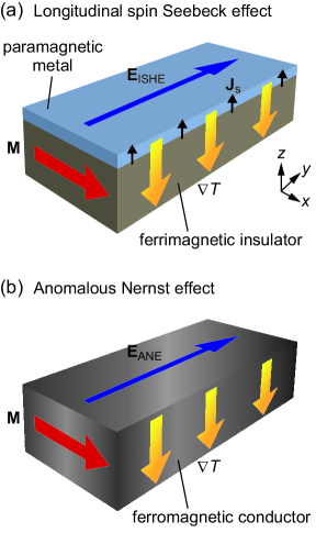
The observation of the LSSE has typically been reported in Pt/YIG systems SSE5 ; SSE13 . However, in this conventional structure, since Pt is near the Stoner ferromagnetic instability Ibach ; DOS , ferromagnetism may be induced in the Pt layer in the vicinity of the Pt/YIG interface due to a static proximity effect, although the magnetization of YIG is so small that the proximity is expected to be weak. Against this backdrop, Huang et al. Chien pointed out that the LSSE voltage in the Pt/YIG structure might be contaminated by the anomalous Nernst effect (ANE) Nernst due to the magnetic proximity in the Pt layer [compare Figs. 1(a) and 1(b)] and that the exclusive establishment of the LSSE is necessary. In this letter, to do that, we provide clear evidence for the existence of the LSSE free from the ANE induced by the proximity effect. First, we show that the LSSE appears even in Au/YIG and Pt/Cu/YIG structures; since Au and Cu are typical metals far from the Stoner instability Ibach ; DOS , the observation of the LSSE in these structures allows us to conclude that the LSSE is an intrinsic phenomenon and different from the proximity ANE. Second, we demonstrate that the LSSE can be distinguished from the ANE by comparing the voltages in different magnetization and temperature-gradient configurations and that the ANE contamination is negligibly small even in the Pt/YIG structure.
First of all, we measured Hall effects in a Au/YIG structure. Here, a 4.5-m-thick single-crystalline YIG (111) film was grown on a 0.5-mm-thick Gd3Ga5O12 (GGG) (111) substrate by a liquid phase epitaxy method, where the resistance of the YIG film is much greater than the measurement limit of our electrometer: 210 G. A 10-nm-thick Au Hall bar was then deposited on the surface of the YIG film [Fig. 2(a)]. As shown in Fig. 2(c), the Hall resistivity in the Au/YIG sample varies linearly with respect to the magnitude of an external magnetic field applied perpendicular to the Au/YIG interface due to the normal Hall effect in Au. We found that the dependence of the Hall resistivity in the Au/YIG sample completely coincides with that in a Au/GGG sample, where the Au Hall bar was fabricated directly on a paramagnetic GGG substrate [Figs. 2(c) and 2(d)]. The same behavior was observed at temperatures ranging from 300 to 2 K [see the inset to Fig. 2(d)]. These results confirm that the Au film on YIG exhibits no anomalous Hall effect, a situation enabling the detection of the intrinsic LSSE free from the magnetic proximity.
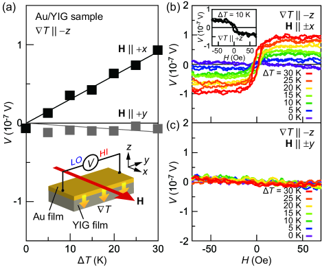
Now we focus on the LSSE in the Au/YIG structure. To measure the LSSE, we used the Au/YIG sample with a 7 6 mm2 rectangular shape, where the whole surface of the YIG film is covered with the Au film. A temperature gradient was applied perpendicular to the Au/YIG interface. Here, the temperatures of the top of the Au film and the bottom of the GGG substrate were stabilized, respectively, at and . During the LSSE measurements, a magnetic field was applied along the or direction; the magnetization of the YIG film is aligned along the in-plane direction when . Under this condition, we measured an electric voltage between the ends of the Au layer along the direction.
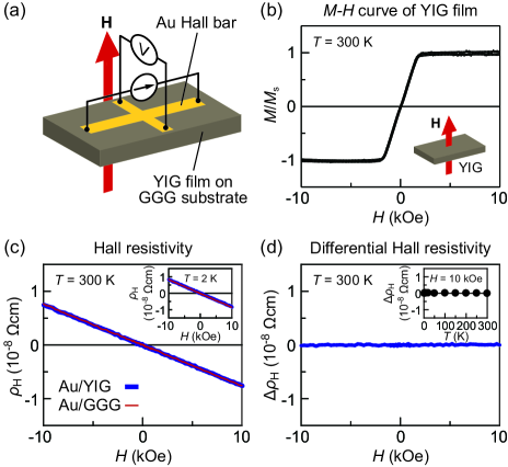
Figure 3(a) shows the measured in the Au/YIG sample at as a function of the temperature difference . When was applied along the direction, the signal was observed to be proportional to . We confirmed that the sign of the signal is reversed by reversing [Fig. 3(b)] and that the signal disappears when is along the direction [Figs. 3(a) and 3(c)]. By reversing the direction, the sign of is also reversed [see the inset to Fig. 3(b)]. This behavior of the signal in the Au/YIG sample is the characteristic of the ISHE voltage induced by the LSSE. Since Au is a typical metal far from ferromagnetism, this result shows that the LSSE appears even in the absence of the proximity ANE.
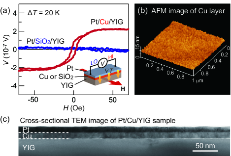
Next, we show that the LSSE appears also in the Pt/Cu/YIG structure, where a Cu film is inserted between Pt and YIG films to block the possible induced ferromagnetism in Pt. The thickness of the Cu interlayer is 13 nm; this is thick enough to eliminate the magnetic proximity between Pt and YIG, while the LSSE voltage can persist in the Pt layer owing to the long spin-diffusion length of Cu ISHE3 . We checked that the surface roughness of the Cu interlayer is smaller than 1 nm by means of atomic force microscopy [Fig. 4(b)] and transmission electron microscopy [Fig. 4(c)], a result showing that the Pt/Cu/YIG sample has no pinholes in the Cu interlayer and no leaked magnetic proximity between the Pt and YIG layers. As shown in Fig. 4(a), we also observed a clear signal in the Pt/Cu/YIG sample, providing further evidence for the existence of the intrinsic LSSE since Cu is also free from induced ferromagnetism. In contrast, we found that the signal disappears in a Pt/SiO2/YIG sample, where the Cu layer is replaced by an insulating 10-nm-thick SiO2 film [Fig. 4(a)]. This result confirms that 10 nm is thick enough to eliminate the magnetic proximity between Pt and YIG and that the direct contact between YIG and metal is necessary for generating the spin current, consistent with the scenario of the LSSE.
The above experiments in the Au/YIG and Pt/Cu/YIG samples clearly show the existence of the intrinsic LSSE free from the ANE. Then, is the voltage signal in the conventional Pt/YIG structure contaminated by the proximity ANE? The following experiments provide a clear-cut answer to this question.
The LSSE in the Pt/YIG structure can be separated from the ANE by comparing voltage in an in-plane magnetized (IM) configuration (the conventional LSSE setup) and a perpendicularly magnetized (PM) configuration in which was applied in the Pt-film-plane direction [compare Figs. 5(a) and 5(b)]. In the PM configuration, the ANE voltage can appear, while the LSSE voltage should disappear due to the ISHE symmetry, enabling the estimation of the ANE contamination in the Pt/YIG structure [see Eq. (1) and note that in the PM configuration]. To compare voltage signals between the IM and PM configurations, we used a Pt-film/YIG-slab sample that comprises a single-crystalline YIG slab with the size of mm3 covered with a 10-nm-thick Pt film, without substrates to avoid a thermal-conductivity-mismatch problem SSE11 ; SSE13 . Then, the sample was sandwiched between two large Cu blocks of which the temperatures were stabilized at and to apply a uniform temperature gradient to the sample [Fig. 5(b)]. In the IM (PM) configuration, was applied along the () direction. As shown in Fig. 5(d), we found that the magnetic field of is also large enough to align the magnetization of the YIG slab along the direction in the PM configuration, since the YIG sample used here is a thick slab. Note that, in the PM configuration, even a possible tiny temperature gradient perpendicular to the Pt-film plane does not affect the voltage signal, since the Nernst voltage is not generated due to the collinear orientation of the perpendicular temperature gradient and .
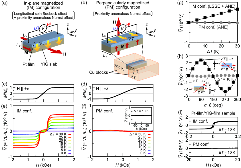
Figures 5(e) and 5(f), respectively, show the dependence of in the Pt-film/YIG-slab sample for various values of in the IM and PM configurations, measured when was applied perpendicular to both and the longest direction of the sample. Here, denotes the voltage including geometric factors: with being the length of the sample in the temperature-gradient (interelectrode) direction [Figs. 5(a) and 5(b)] that enables the quantitative comparison of the signals between the IM and PM configurations. We found that the signal in the Pt-film/YIG-slab sample in the PM configuration is much smaller than that in the IM configuration [compare Figs. 5(e) and 5(f) and see also Figs. 5(g) and 5(h)]. The ratio of the voltage magnitude between the IM and PM configurations is estimated to be at each , where denotes in the IM (PM) configuration at . This result indicates that the ANE contamination in the Pt/YIG sample is, if any, less than 5 % of the voltage signal, since potentially contains both the proximity ANE and leaked SSE voltages due to experimental errors, i.e., minimal inclination of the direction. We also observed similar behavior of in a Pt-film/YIG-film sample on a GGG substrate [Fig. 5(i)]. All the results shown above confirm that the voltage signal observed in the IM configuration is due almost entirely to the ISHE voltage induced by the LSSE.
In conclusion, we report experiments for the exclusive detection of the LSSE. First, we observed the LSSE in the Au/YIG and Pt/Cu/YIG structures. Since Au and Cu are far from the Stoner ferromagnetic instability, these observations confirm the existence of the LSSE free from the ANE induced by the magnetic proximity. In the conventional Pt/YIG structure, the voltage measurements in the in-plane and perpendicularly magnetized configurations show that the LSSE provides a dominant contribution and that the ANE contamination is negligibly small. Whether or not proximity ferromagnetism exists in Pt cannot be discussed based on the present results. However, we can conclude that the observed LSSE voltage is at least irrelevant to the proximity ANE.
The authors thank Y. Sakuraba and K. Takanashi for their assistance in magnetometry measurements. This work was supported by PRESTO-JST “Phase Interfaces for Highly Efficient Energy Utilization”, CREST-JST “Creation of Nanosystems with Novel Functions through Process Integration”, a Grant-in-Aid for Research Activity Start-up (24860003) from MEXT, Japan, a Grant-in-Aid for Scientific Research (A) (24244051) from MEXT, Japan, LC-IMR of Tohoku University, the Murata Science Foundation, the Mazda Foundation, the Sumitomo Foundation, and MOST (No. 2011CB921802).
References
- (1) K. Uchida, S. Takahashi, K. Harii, J. Ieda, W. Koshibae, K. Ando, S. Maekawa, and E. Saitoh, Nature 455, 778 (2008).
- (2) J. Xiao, G. E. W. Bauer, K. Uchida, E. Saitoh, and S. Maekawa, Phys. Rev. B 81, 214418 (2010).
- (3) K. Uchida et al., Nat. Mater. 9, 894 (2010).
- (4) C. M. Jaworski, J. Yang, S. Mack, D. D. Awschalom, J. P. Heremans, and R. C. Myers, Nat. Mater. 9, 898 (2010).
- (5) K. Uchida, H. Adachi, T. Ota, H. Nakayama, S. Maekawa, and E. Saitoh, Appl. Phys. Lett. 97, 172505 (2010).
- (6) H. Adachi, K. Uchida, E. Saitoh, J. Ohe, S. Takahashi, and S. Maekawa, Appl. Phys. Lett. 97, 252506 (2010).
- (7) H. Adachi, J. Ohe, S. Takahashi, and S. Maekawa, Phys. Rev. B 83, 094410 (2011).
- (8) C. M. Jaworski, J. Yang, S. Mack, D. D. Awschalom, R. C. Myers, and J. P. Heremans, Phys. Rev. Lett. 106, 186601 (2011).
- (9) S. Bosu, Y. Sakuraba, K. Uchida, K. Saito, T. Ota, E. Saitoh, and K. Takanashi, Phys. Rev. B 83, 224401 (2011).
- (10) K. Uchida, H. Adachi, T. An, T. Ota, M. Toda, B. Hillebrands, S. Maekawa, and E. Saitoh, Nat. Mater. 10, 737 (2011).
- (11) K. Uchida, T. Ota, H. Adachi, J. Xiao, T. Nonaka, Y. Kajiwara, G. E. W. Bauer, S. Maekawa, and E. Saitoh, J. Appl. Phys. 111, 103903 (2012).
- (12) A. Kirihara, K. Uchida, Y. Kajiwara, M. Ishida, Y. Nakamura, T. Manako, E. Saitoh, and S. Yorozu, Nat. Mater. 11, 686 (2012).
- (13) J. C. Slonczewski, J. Magn. Magn. Mater. 159, L1 (1996).
- (14) Spin Current, edited by S. Maekawa, E. Saitoh, S. O. Valenzuela, and T. Kimura (Oxford University Press, Oxford, 2012).
- (15) S. A. Wolf, D. D. Awschalom, R. A. Buhrman, J. M. Daughton, S. von Molnar, M. L. Roukes, A. Y. Chtchelkanova, and D. M. Treger, Science 294, 1488 (2001).
- (16) I. Žutić, J. Fabian, and S. Das Sarma, Rev. Mod. Phys. 76, 323 (2004).
- (17) Concepts in Spin Electronics, edited by S. Maekawa (Oxford University Press, Oxford, 2006).
- (18) M. Johnson and R. H. Silsbee, Phys. Rev. B 35, 4959 (1987).
- (19) G. E. W. Bauer, E. Saitoh, and B. J. van Wees, Nat. Mater. 11, 391(2012).
- (20) E. Saitoh, M. Ueda, H. Miyajima, and G. Tatara, Appl. Phys. Lett. 88, 182509 (2006).
- (21) S. O. Valenzuela and M. Tinkham, Nature 442, 176 (2006).
- (22) T. Kimura, Y. Otani, T. Sato, S. Takahashi, and S. Maekawa, Phys. Rev. Lett. 98, 156601 (2007).
- (23) K. Ando et al., J. Appl. Phys. 109, 103913 (2011).
- (24) R. Takahashi, R. Iguchi, K. Ando, H. Nakayama, T. Yoshino, and E. Saitoh, J. Appl. Phys. 111, 07C307 (2012).
- (25) H. Nakayama, K. Ando, K. Harii, T. Yoshino, R. Takahashi, Y. Kajiwara, K. Uchida, Y. Fujikawa, and E. Saitoh, Phys. Rev. B 85, 144408 (2012).
- (26) H. Ibach and H. Luth, Solid-State Physics: An Introduction to Principles of Materials Science (Springer, Berlin, 2009).
- (27) D. A. Papaconstantopoulos, Handbook of the Band Structure of Elemental Solids (Plenum Press, New York, 1986).
- (28) S. Y. Huang, X. Fan, D. Qu, Y. P. Chen, W. G. Wang, J. Wu, T. Y. Chen, J. Q. Xiao, and C. L. Chien, Phys. Rev. Lett. 109, 107204 (2012).
- (29) W. Nernst, Ann. Phys. 267, 760 (1887).