Induced superconductivity in the three-dimensional topological insulator HgTe
Abstract
A strained and undoped HgTe layer is a three-dimensional topological insulator, in which electronic transport occurs dominantly through its surface states. In this Letter, we present transport measurements on HgTe-based Josephson junctions with Nb as superconductor. Although the Nb-HgTe interfaces have a low transparency, we observe a strong zero-bias anomaly in the differential resistance measurements. This anomaly originates from proximity-induced superconductivity in the HgTe surface states. In the most transparent junction, we observe periodic oscillations of the differential resistance as function of an applied magnetic field, which correspond to a Fraunhofer-like pattern. This unambiguously shows that a precursor of the Josephson effect occurs in the topological surface states of HgTe.
pacs:
73.23.-b, 73.25.+i, 72.80.Ey, 74.45.+cTopological insulators (TIs) are a recently discovered new class of materials TI-RMP . In two dimensions (2-D), a TI is an insulating material with conducting helical states at its edges. The first experimental realization of a 2-D TI was a HgTe quantum well, in which the topological state of matter was unambiguously demonstrated by the observation of the quantum spin Hall effect in electronic transport experiments 07-KOE . The first three-dimensional (3-D) TIs, Bi1-xSbx, Bi2Se3 and Bi2Te3, were discovered soon after 3D-TI . 3-D TIs are bulk insulators with conducting states at their surfaces. Since these surface states are effectively described by Dirac Hamiltonians, the corresponding quasiparticles behave as chiral Dirac fermions, i.e. the spin and momentum of the electrons are locked TI-RMP .
Recently, it has been predicted that, due to the superconducting proximity effect, a Dirac fermion at the surface of a 3-D TI can be split into two so-called Majorana quasiparticles 08-FU . These are zero-energy bound states that may be present at the surface when a TI is contacted by a superconductor. The realization of a superconductor-topological insulator-superconductor (S-TI-S) junction is an important first step to study the existence of Majorana fermions. S-TI-S junctions based on Bi2Se3 11-SAC and Bi2Te3 11-VEL have been recently reported and a Josephson supercurrent has been observed in both these 3-D TIs. However, since the Bi-based 3-D TIs have a large density of states in their bulk, only a small part of the observed supercurrent can be attributed to superconducting correlations in the surface states. We recently demonstrated that strained HgTe is a 3-D TI with negligible bulk conductance when the Fermi level is inside its bandgap 11-BRU . This material is thus a more promising candidate to study the Josephson effect in S-TI-S junctions without being hindered by bulk states.
In this Letter, we study electronic transport through S-TI-S junctions based on superconducting Nb wires contacted to a strained HgTe layer, in which the electrical conduction is dominated by surface state transport. Although it turns out that the Nb-HgTe interfaces have a low transparency, we clearly observe induced superconductivity and transport through surface states approaching the supercurrent regime. Our results provide clear evidence of superconducting correlations in the topological surface states of HgTe.
Two bulk HgTe layers of 50 and 70 nm thickness, respectively, are grown by molecular beam epitaxy on a CdTe substrate. The samples are etched in an Ar plasma to obtain 2 m wide HgTe stripes. On the top surface of the HgTe stripes, 68 nm thick Nb superconducting wires are deposited by using ultra high vacuum sputtering and lift-off techniques. Each pair of closely-spaced neighboring wires forms an S-TI-S junction (Figs. 1a, b). The transport measurements on these devices have been performed at dilution refrigerator temperatures. We have measured the differential resistance of the junctions as function of magnetic field and current bias by using standard lock-in detection techniques. Here we will discuss the data of two of the closest junctions with 150 nm contact spacing; other junctions show consistent behaviour.
In a first set of measurements we investigate the superconductiong properties of the 50 nm thick HgTe layer. In order to characterize the transport properties of this bulk HgTe layer, we have fabricated from the same wafer as used for one of the S-TI-S junctions, a large six-terminal Hall bar with a channel length of 600 m and width of 200 m (similar to the device reported in Ref. 11-BRU ). From the longitudinal and transversal magnetoresistance measurements at K, we extract an electron density of cm-2 and a mobility of cm2/Vs. These values are typical for strained HgTe layers in which electronic transport is dominantly through their Dirac surface states 11-BRU . Moreover, at magnetic fields higher than 2 T we observe a series of quantization steps in the Hall resistance, indicating that transport is indeed occurring through 2-D states SI ; 12-SHU .
Since the transport is dominated by surface states, it is possible to investigate the behavior of a S-TI-S junction, fabricated on this same 50 nm thick layer. In order to study transport in the superconducting regime, we have performed two-terminal measurements at a base temperature of mK (which is far below the experimentally verified critical temperature of Nb, 9 K). Since each Nb terminal is split into two leads one for current injection and the other for voltage measurement we can simultaneously measure the differential resistance of the junction and the electrochemical potential difference between the Nb contacts (Fig. 1b). The differential resistance () as a function of the measured voltage across the junction () provides detailed information about the energy dependence of the transmission probability of quasiparticles through the junction Tinkham .
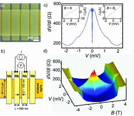
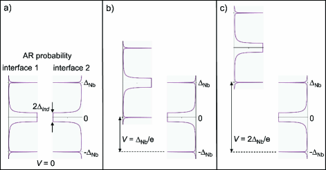
Fig. 1c shows as function of for one of the junctions at zero magnetic field. At 2 mV, we observe a pronounced dip in . This is when the potential difference between both Nb contacts equals twice the superconducting gap ( 1 meV). When , the upper band edge of the quasiparticle states in one Nb lead is aligned with the lower band edge of the other (Fig. 2c). At these energies, the quasiparticle density of states in the Nb as well as the Andreev reflection (AR) probability is enhanced OBTK , which gives rise to an increased transmission probability at both interfaces, and thus a decrease of the differential resistance of the junction Tinkham .
For mV, when the potential difference between the Nb contacts is larger than , the differential resistance is 200 . This is the normal conductivity transport regime, where the superconducting gaps of the Nb leads have no energy overlap and single quasiparticles from filled states below the gap in one lead are transmitted to empty states above the gap in the other lead.
If , the superconducting gaps of the Nb leads have an energy overlap. In this sub-gap regime, quasiparticles can only be transmitted through the junction by AR processes at the interfaces OBTK . Fig. 1c shows that below mV a strong increase of the differential resistance occurs on lowering the voltage difference between the Nb leads . This indicates that the AR probability is suppressed due to the low transparency of the Nb-HgTe interfaces.
A further characterization of the junction is done by measuring the magnetic field dependence of the versus characteristics (Fig. 1d). At perpendicular magnetic fields () larger than 3 T, we observe a steep increase in the differential resistance, which is due to the transition of Nb from superconducting to normal state. If the magnetic field is decreased below 3 T, the superconducting gap opens and the band edge can be probed by measuring the corresponding dip at as function of magnetic field (Fig. 3a). This dip, where , is visualized in a colorplot by numerically differentiating versus and plotting the obtained absolute value versus and the applied magnetic field (Fig. 3b). The figures clearly show that the gap increases from 0 to 1 meV when the magnetic field decreases from 3 to 0 T.
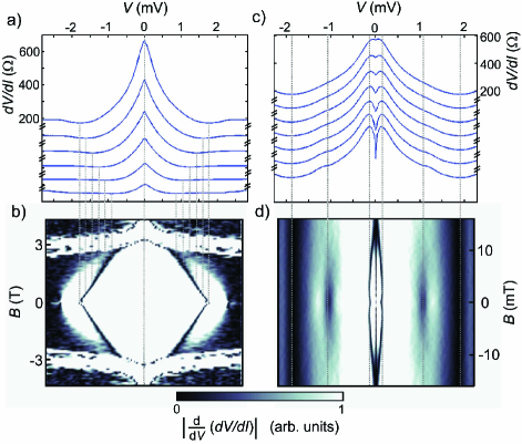
Interestingly, Fig. 1c shows a strong dip in at very small bias. Figs. 3c, d show that this zero-bias anomaly (ZBA) appears at 100 V and 10 mT. A ZBA can appear in Josephson junctions due to the superconducting proximity effect in the normal conductor ZBA . Also in our S-TI-S junction, Cooper pairs ”leak” from the Nb into the HgTe below the contacts, yielding electron correlations in the surface states 10-STA .These correlations give rise to induced superconductivity on an energy scale of the order of the induced superconducting gap () which depends on the transparency of the contacts. The fact that the observed ZBA is very strong indicates the surface character of the induced superconductivity in HgTe SI . In conventional materials with bulk transport, the ZBA is usually much weaker due to the decay of the correlations with distance from the superconductor ZBA . When the bias across the junction is smaller than twice the induced gap (), the AR probability at each interface is strongly enhanced (Fig. 2a), yielding a large suppression of the differential resistance. In our junction, the ZBA appears below 100 V (Figs. 4a, b), indicating an induced superconducting gap of 50 eV, which is close to a theoretically expected value for the topological surface states of HgTe SI .
The ZBA completely disappears when a perpendicular magnetic field of 10 mT is applied. A magnetic field gives rise to a phase gradient in the order parameter and induces screening currents in the Nb MovCond , as has been previously observed in Nb/InAs Josephson junctions 09-ROH . The moving condensate leads to momentum and energy transfer in AR processes, resulting in a Doppler shift of the energy of an Andreev reflected quasiparticle with respect to the incoming quasiparticle. When this Doppler shift becomes comparable to the ZBA will disappear MovCond . In our junction, this occurs at a magnetic field value of 10 mT (Figs. 3c, d and 4b), which is of the same order as the estimated value obtained from calculations SI .
When we consider the sub-gap regime of the versus characteristic in Fig. 1c more carefully, we observe a feature at 1 mV. Its position corresponds approximately to the value of the superconducting gap in Nb ( 1 meV). At this bias voltage, the band edge of one Nb lead is aligned with the center of the gap of the other lead. This alignment leads to an increase of the transmission probability through the junction due to the enhanced AR probability at both interfaces (Fig. 2b). The observed kink in at is therefore closely related to the ZBA. Fig. 3c, d show that this feature indeed disappears at a magnetic field larger than 10 mT, similar to the scale associated with the disappearance of the ZBA.
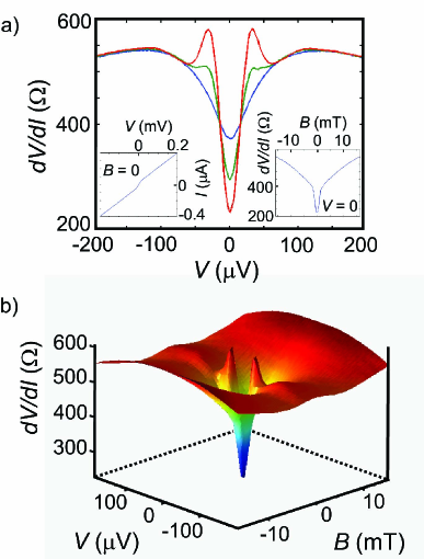
So far, we have shown that the Nb contacts induce superconductivity in this HgTe system. These electron correlations occur at least below each contact. If electron transport through the HgTe between both Nb contacts is phase coherent, the Josephson effect should give rise to bound states through which a supercurrent can flow. The critical value of such a current () depends on the phase difference between the condensates in both Nb layers 62-JOS . We do not, however, observe a dissipationless current, indicating that it is destroyed by phase decoherence mechanisms. A supercurrent is absent if the thermal energy of the electromagnetic noise is larger than the Josephson energy Tinkham , which can occur when the wires leading to the sample are not sufficiently filtered and shielded Filtering . Given the incomplete filtering in our present set-up, this my well explain the absence of a supercurrent. However, the signature of a crossover towards a Josephson supercurrent is already visible in Figs. 4a, b, where we observe an enhanced suppression of the differential resistance when 40 V and 1 mT.
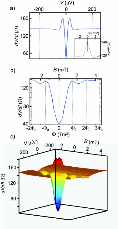
To further investigate the ZBA, we have fabricated a second array of S-TI-S junctions. The junctions have the same geometry, but the contact interfaces have been improved by a modified fabrication process. After e-beam patterning and development, we have now cleaned the HgTe surface by exposing it to a very mild, low-power, Ar plasma prior to Nb sputtering. This plasma cleaning results in more transparent Nb-HgTe interfaces without affecting the quality of the surface states. This device has been fabricated on a similar HgTe layer of 70 nm thickness SI . The differential resistance of this junction (see inset of Fig. 5a) has a smaller increase in the subgap region ( mV), indicating a smaller tunnel barrier at the interfaces. The ZBA appears at a higher bias value than in the previous sample (at 200 ; see dotted line in Fig. 5a), consistent with a larger induced gap, as expected for more transparent contacts. Also the zero-bias value of (with respect to ) is much smaller than in the previous sample.
That we are approaching the supercurrent regime is convincingly shown by measurements of the differential resistance as function of magnetic field (Figs. 5b, c). At zero-bias, we observe an oscillating behaviour of with maxima at for (see dotted lines in Fig. 5b), and minima for (with mT). This periodic behaviour is closely related to a Fraunhofer pattern that is usually observed in the supercurrent regime of a Josephson junction Tinkham , and which shows the presence of a uniform current through proximity-induced coherent states between the two Nb contacts. The effective area () can be determined from the periodicity of the oscillations, and is equal to 1.3 m2 (where is the flux quantum). The width of the HgTe stripe is 2 m, giving an effective length of 650 nm, which is approximately equal to the distance between the centers of the Nb leads. This result clearly shows that a precursor of the Josephson effect occurs in the topological surface states of strained HgTe.
Acknowledgements.
We thank C. Ames, P. Leubner, M. Mühlbauer, and C. Thienel for fabrication and characterization of the HgTe layers, and B. Trauzettel and P. Recher for useful discussions. This work was financially supported by the German research foundation DFG [SPP 1285 Halbleiter Spintronik, DFG-JST joint research program ’Topological Electronics’, Emmy-Noether Grant, No. HA5893/3-1], and the EU ERC-AG program [project 3-TOP].References
- (1) M. Z. Hasan, C. L. Kane, Rev. Mod. Phys. 82, 3045 (2010); X. L. Qi, S. Z. Zhang, Rev. Mod. Phys. 83, 1057 (2011).
- (2) M. König et al., Science 318, 766 (2007).
- (3) D. Hsieh et al., Nature 452, 970 (2008); Y. Xia et al., Nat. Phys. 5, 398 (2009); Y. L. Chen et al., Science 325, 178 (2009).
- (4) L. Fu, C. L. Kane, Phys. Rev. Lett. 100, 096407 (2008).
- (5) B. Sacépé et al., Nat. Commun. 2:575, doi: 10.1038/ncomms1586 (2011); J. R. Williams et al., Phys. Rev. Lett. 109, 056803 (2012).
- (6) M. Veldhorst et al., Nat. Mater. 11, 417 (2012).
- (7) C. Brüne et al., Phys. Rev. Lett. 106, 126803 (2011).
- (8) See Supplemental Online Material.
- (9) A. M. Shuvaev et al., arXiv: 1208.1115 (2012).
- (10) M. Tinkham, Introduction to Superconductivity (McGraw-Hill, New York, 1996).
- (11) M. Octavio, M. Tinkham, G. E. Blonder, T. M. Klapwijk, Phys. Rev. B 27, 6739 (1983).
- (12) B. Pannetier, H. Courtois, J. Low Temp. Phys. 118, 599 (2000); T. M. Klapwijk, J. Supercond. 17, 593 (2004).
- (13) T. D. Stanescu, J. D. Sau, R. M. Lutchyn, S. Das Sarma, Phys. Rev. B 81, 241310(R) (2010).
- (14) A. F. Volkov, T. M. Klapwijk, Phys. Lett. A 168, 217 (1992); M. Fogelström, D. Rainer, J. A. Sauls, Phys. Rev. Lett. 79, 281 (1997); G. Tkachov, V. I. Fal’ko, Phys. Rev. B 69, 092503 (2004).
- (15) F. Rohlfing et al., Phys. Rev. B 80, 220507(R) (2009).
- (16) B. D. Josephson, Phys. Lett. 1, 251 (1962).
- (17) P. Jarillo-Herrero, J. A. van Dam, L. P. Kouwenhoven, Nature 439, 953 (2006); H. I. Jorgensen, K. Grove-Rasmussen, T. Novotny, K. Flensberg, P. E. Lindelof, Phys. Rev. Lett. 96, 207003 (2006).