An experimental study of charge distribution in crystalline and amorphous Si nanoclusters in thin silica films
Abstract
Crystalline and amorphous nanoparticles of silicon in thin silica layers were examined by transmission electron microscopy (TEM), electron energy loss spectroscopy (EELS) and x-ray photoelectron spectroscopy (XPS). We used XPS data in the form of the Auger parameter to separate initial and final state contributions to the Si2p energy shift. The electrostatic charging and electron screening issues as well as initial state effects were also addressed. We show that the chemical shift in the nanocrystals is determined by initial state rather than final state effects, and that the electron screening of silicon core holes in nanocrystals dispersed in SiO2 is inferior to that in pure bulk Si.
I Introduction
I.1 Si nanoparticles in SiO2
Drastic changes in materials properties and performance take place upon reduction of size and dimensionality of crystals and nanostructures. This has been the driving force in research and development of nanoscaled MOS (Metal-Oxide-Semiconductor) devices used for memory storage applications Kapetanakis et al. (2000); Boer et al. (2001). Investigations on silicon nanocrystals (NCs) in silica matrices Tiwari et al. (1996a) have been motivated by the possibility of replacing the original bulk-floating gate and applications Pavesi and Lockwood (2004) such as nanocrystal memory cellsTiwari et al. (1996b), photon converters and optical amplifiers Han et al. (2002); Kik and Polman (2002). The main expectations include longer retention, lower gate voltage and lower power consumption Chen et al. (2004). In addition, the discontinuity between the nanocrystals can prevent lateral charge loss and can also result in short writing times at lower voltages, as well as improved reliability Karadas et al. (2004); Lombardo et al. (2004). Both injection and retention of electrons in these devices are very sensitive to the size, distribution, interfaces and electronic structure of the nanocrystals. Appropriate combination of these parameters may lead to dramatic improvements in device performances Blauwe (2002).
I.2 The Si2p-shift in elemental silicon - earlier studies
There is a significant number of studies on the Si/SiO2 system referring to planar or curved interfaces (particles in an oxide matrix), using XPS data. The majority of them was focused on the position and energy shift of the Si peak (were Si0 is Si in elemental state) Chen et al. (2004); Eickhoff et al. (2005); Iwata and Ishizaka (1996); Sun et al. (2003a, b). Studies of the planar SiO2/Si(100) interface, attributed the shift either to final state relaxation effectsEickhoff et al. (2005) or to enhanced differential charging by application of a negative bias to the substrateKaradas et al. (2004). Sun et al. Sun et al. (2003a) concluded that the shift is a result of an enlargement of the band gap due to surface imperfections at the Si nanocrystal-oxide interface. In a comprehensive paper from Iwata and IshizakaIwata and Ishizaka (1996) on planar SiO2/Si interfaces, the shift was interpreted as a result of charging, that was dependent on x-ray intensity, time and sample thickness. They briefly mentioned that Auger parameters are independent of charging, without showing any implicit data. In a recent study, Dane et al. Dane et al. (2006) ascribed the shift in the Si binding energy of Si nanoclusters to relaxation energy differences measured by the final state Auger parameter.
I.3 XPS chemical shift, the Auger parameter and chemical state diagrams
X-ray Photoelectron Spectroscopy (XPS) is commonly used as a surface analysis technique to characterize chemical states of surfaces and interfaces. It is also frequently used for studying the electronic structure of materials. Interpretation of XPS spectra are often based on shifts of peak positions and Auger parameters Evans et al. (1992); Mejias et al. (1997). The peak shift between two different chemical environments is known as chemical shift and is defined as the binding energy difference () between atoms bonded to different chemical species, e.g. elemental Si and SiO2 (EB Si4+ - EB Si0). However, determination of chemical shifts depend on reliable measurements of XPS peak positions, which in turn are sensitive to energy referencing issues. Additional difficulties arise when measurements are performed on different samples or spectrometers and/or by using different experimental setups. Interpretations of the chemical shift are often complicated by differential charging when the sample is partially (semi)conducting and partially insulating. In addition, chemical shifts (in the form of binding or kinetic energy differences) contain both initial and final state contributions, as shown by equations 1 and 2 belowEvans et al. (1992).
| (1) |
and
| (2) |
where () and () are the shifts in the photoelectron binding and Auger electron kinetic energy respectively. In the above formulas V reflects initial state changes in the atomic potential arising from changes in valence electron charge and/or Coloumb interactions at the emission site. The term expresses changes in the work function and R refers to final state changes associated with relaxation/core hole screening energy.
The use of the Auger parameter (), as defined by equation 3 eliminates energy referencing problems Wagner (1975).
| (3) |
The combination of equations 1, 2 and 3 leads to two different Auger parameter expressions reflecting either initial or final state effects; the initialEvans et al. (1992) () and final stateGaarenstrom and Winograd (1977); Thomas and Weightman (1986) () Auger parameter respectively:
| (4) |
and
| (5) |
The final state Auger parameter () which is free of energy referencing problems, measures reliably the response of the system to the core hole electron screening Walker et al. (1994); Matthew et al. (1995). The initial state Auger parameter is not completely independent of energy referencing due to the triple weighting of the binding energy () in its definition.
Very often chemical state or Wagner diagrams are employed to facilitate visualization and subsequent interpretation of the and valuesWagner (1975); Moretti (1998). In the case of e.g. Si, such a diagram is constructed by plotting the binding energy of the Si2p peak against the kinetic energy of the SiKLL peak. The Auger kinetic energy is on the ordinate and the photoelectron binding energy is on the abscissa oriented in the negative direction. The Auger parameters are then expressed by the linear relationship EK (Auger peak) versus EB (photoemission peak) and lie on the straight lines with slope +1 (final state ) and +3 (initial state) Moretti (1998). This means that all points lying on each line correspond to the same Auger parameter value.
Due to the variety of results and explanations concerning the Si 2p shift (see section B above), we attempt a detailed study of the mechanisms resulting in the Si 2p shift using photoelectron spectroscopy data in the form of the SiKLL-Si2p Auger parameter and chemical state (Wagner) plots, high resolution transmission electron microscopy (HRTEM) and electron energy loss spectroscopy (EELS). Electron Energy Loss Spectroscopy (EELS) is a useful tool in studying the electronic structure of nanostructural features of materials. Changes in the Si plasmon peak energy (due to valence electron vibrations) have been previously attributed to changes in quantum confinement and/or changes in the energy band gap Mitome et al. (1992).
II Materials and methods
The samples were produced by growing a 3 nm layer of SiO2 on a p-type silicon substrate by rapid thermal oxidation (RTO) at 1000oC for 6 sec. Prior to growing the RTO layer the wafers were cleaned using a RCA (Radio Corporation of America) standard procedure for removing contaminants, followed by immersion in a 10 % HF solution to remove the native oxide. A 10 nm layer of silicon rich oxide was then sputtered from a SiO2:Si composite target onto the RTO-SiO2 and subsequently heat-treated in N2 atmosphere at 1000-1100oC for 30-60 min. Different percentages of sputtered material area coverage were achieved (Si:SiO2 = 6, 8, 17, 42, 50, 60, 70%), yielding different silicon supersaturation levels in the oxide. Table 1 gives information on the samples studied, their Si content and the applied heating duration and temperature. Cross-sectional TEM samples were prepared by ion-milling using a Gatan precision ion polishing system with a 5 kV gun voltage.
| Nr. in | area % | Heating | Heat-treatment |
|---|---|---|---|
| Wagner | Si | time | temperature |
| diagram (Fig. 6) | (min) | (oC) | |
| 1 | 100111Reference samplePowell and Jablonski (2000) | ||
| 2 | 100222Substrate | 30 | 1000 |
| 3 | 50 | 00 | 00 |
| 4 | 60 | 00 | 00 |
| 5 | 70 | 00 | 00 |
| 6 | 28 | 30 | 1000 |
| 7 | 42 | 30 | 1000 |
| 8 | 42 | 60 | 1100 |
| 9 | 50 | 30 | 1000 |
| 10 | 50 | 120 | 1000 |
| 11 | 60 | 30 | 1000 |
| 12 | 70 | 30 | 1000 |
| 13 | 70 | 60 | 1000 |
| 14 | 70 | 60 | 1100 |
The Si nanoparticles (in crystalline and amorphous state) were observed by HRTEM and/or by energy filtered TEM- spectral imaging (EFTEM-SI) of the plasmon peak. HRTEM was performed with a 300 keV JEOL JEM-3100FEF TEM equipped with an Omega imaging filter. For EELS, a 200 keV JEOL 2010F TEM with a Gatan imaging filter and detector was used. Energy filtered images were acquired by filtering the plasmon peak of silicon (16.8 eV) with an energy slit of 2 eV. XPS was performed using a VG Scientific ESCALAB MkII fitted with a Thermo Electron Corporation Alpha 110 electron energy analyser, with non-monochromatic AlKa radiation on plan view samples at a take-off angle of 45o. Survey scans and high resolution spectra were acquired using pass energies of 100 and 20 eV respectively. Non-monochromatic radiation was employed as it is the Bremsstrahlung component of the radiation from this type of source that is responsible for the excitation of the SiKLL transition Castle and West (1979). The inelastic mean free path of the Si2p electrons in SiO2 is about 3.2 nm Powell and Jablonski (2000). A take off angle of 450 results in a photoelectron escape depth of about 7 nm, which allowed us to study the silicon nanoclusters located 5 nm below the surface of the oxide. The spectra were peak fitted using Casa XPS http://www.casaxps.com/ after subtraction of a Shirley type background. The FWHM values used for fitting the various components of the Si2p peak Si, Si2O, SiO, Si2O3 and SiO2 were 1.4 eV, 1.6 eV, 1.9 eV, 1.9 eV and 2.0-2.3 eV respectively.
III Results
III.1 Crystalline and amorphous Si nanoclusters
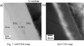
Samples with different area percentages of Si:SiO2 have been systematically studied with HRTEM and energy filtered TEM (EFTEM) in order to relate the volume fraction, size and structure of nanocrystals to processing conditions. The results will be presented elsewhereThøgersen et al. (2006), However, the main findings are briefly summarized in the following two sentences in order to facilitate the discussion in the present work. HRTEM and EFTEM imaging showed presence of nanocrystals 3-8 nm in size in samples with a silicon fraction of 50 % and higher (see also Figure 1). Below 50 % Si, amorphous nanoclusters of 3-6 nm were found.
III.2 Chemical states present in the samples
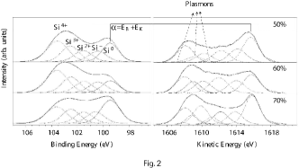
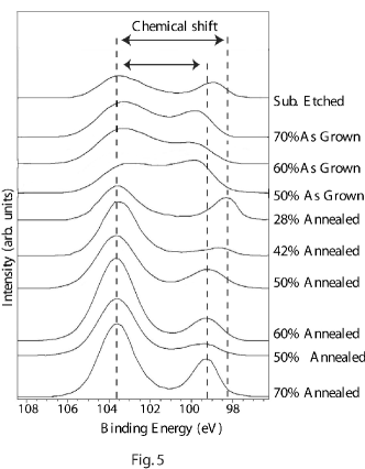
XPS was utilized to identify the oxidation states of Si, detect the amount of elemental Si present in SiO2, possibly as nanocrystals, and relate the shifts in core levels to Si concentration, nanocluster formation and size. Five oxidation states are reported to be present in Si/SiO2 systems, corresponding to the five chemical states Si0, Si2O, SiO, Si2O3 and SiO2 Iwata and Ishizaka (1996); Grunthaner. et al. (1987); Chen et al. (2004). Figure 2 shows the Si2p and SiKLL peaks of three as grown (A.G.) samples with different Si content showing the different chemical states present. The three extra peaks at 1610.9 eV, 1608.7 eV and 1607.8 eV in the SiKLL spectra are plasmon peaks of the Si0, Si+ and Si2+ states and their use optimised peak fitting Jirka (1997); Hirose et al. (2003). The measured final state Auger parameters () of Si0 (EB(Si) = 99.5 eV) and Si4+ (EB(Si) = 103.6 eV) were 1715.4 eV and 1711.2 eV, respectively, in agreement with literature values 1715.7 Smith and Black (1984) for Si0 and 1711.7 eV Wagner et al. (1982) for Si4+.
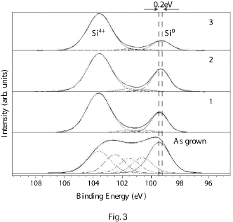
During heat treatment of the as grown samples, the suboxides thermally decomposed to SiO2 and Si0 nanoclusters. It is clear from Figure 3 that annealing decreased the Si3+-, Si2+-, Si+- and Si0- content, and increased that of Si4+. The reduction in intensity of the Si0 peak may be attributed to oxidation due to residual oxygen in the nitrogen atmosphere Chen et al. (2004). Comparison of the as grown sample with the sample annealed at 11000C for 30 min showed that annealing shifted the Si peak position to lower binding energy at 0.2 eV ( 0.1). This decrease in binding energy between the as grown sample and the heat treated sample with a silicon fraction of 70 % is also observed in samples with 50 and 60 % silicon.
III.3 Chemical shifts and nanoparticle size
Table 2 shows that the annealed sample with the highest Si fraction (70%) contained 2.8 at. % of suboxide, whilst the annealed sample with the lowest Si content (28 %) had the highest amount of suboxides 5.3 at. %. Therefore, it seems that the amount of suboxide increases with decreasing Si content and nanocluster size. This is probably an indication of the suboxide being located at the Si nanocluster/silica interface, created by Si ions not fully precipitated into the Si nanoclusters Carrier et al. (2002); Kroll and Schulte (2006); Daldosso et al. (2003).
| area % | Mean | Differential | Chemical | SiOx | |||||
|---|---|---|---|---|---|---|---|---|---|
| Si | diameter | Charging | shift | ||||||
| (nm) | (eV)111Differential charging:((EB(Si4+) - EB(Si)) - (EB(Si0) - EB(Si))) | (eV)222Chemical shift:(EB(Si4+)-EB(Si0)) | (atomic%)333Sum of suboxides | ||||||
| 28 | a-NC | 1.2 | 5.2 | 5.3 | |||||
| 42 | a-NC | 4-6 | 0.8 | 4.9 | 4.5 | ||||
| 50 | c-NC | 4 | 0.2 | 4.4 | 2.7 | ||||
| 60 | c-NC | 4 | 0.1 | 4.3 | 2.0 | ||||
| 50∗ | c-NC | 5 | 0 | 4.2 | 2.4 | ||||
| 70 | c-NC | 4-8 | 0.1 | 4.2 | 2.8 | ||||
| refHimpsel et al. (1988) | 0 | 3.9 | 0 | ||||||
| Sub. | 0.5 | 4.6 | 0 | ||||||
| a-Si444Amorphous, hydrogenated silicon. | -0.4 | 3.8 | 0 | ||||||
| 50 | A.G | -0.9 | 4.1 | 20.7 | |||||
| 60 | A.G. | -0.9 | 4.1 | 26.1 | |||||
| 70 | A.G. | -1.1 | 4.1 | 22.4 |
The Si 2p spectra in Figure 4 (normalized for same Si4+ position) show differences in the chemical shift (Si4+ - Si0) between samples with different fraction of Si (see also Table 2). As grown samples (see also Figure 2) and annealed samples with a Si fraction of 50 % and above showed chemical shifts of 4.1 and 4.3 0.1 eV, respectively. Samples with a lower fraction of Si contained amorphous Si clusters Thøgersen et al. (2006) and showed an increased chemical shift, whilst the measured shift for bulk Si (Si substrate revealed after 2-3 min of Ar etching) was 4.6 eV. These results illustrate a dependence of the shift on whether or not the samples contain amorphous or crystalline nanoclusters and also an increase of the shift with decreasing amorphous nanoclusters size.
III.4 Initial state effects
Binding energy shifts between two different chemical environments contain initial state contributions due to the dependence of the potential on the local environment. They are also influenced by final state variations expressed as the relaxation energy change arising from the response of the local atomic electronic structure to the screening of the core hole. In order to address initial state variations we used the initial state Auger parameter and the Si plasmon peak energies and these values were compared to the measured differential charging.
The difference in electrostatic charging between silicon oxide and silicon nanocrystals/clusters (differential charging) is defined asSun et al. (2003a)
| (6) |
where EB(Si4+) is the Si2p binding energy for SiO2, EB(Si0) is the Si2p binding energy for pure Si, and EB(Si) and EB(Si) are the corresponding reference values Anwar et al. (1990). Differences in Si2p peak positions without corrections for electrostatic charging together with reference values for Si and Si are shown in Table 2 Moulde et al. (1992). The samples containing nanocrystals (Si fraction of 50 % and above), showed the smallest differential charging (0.1 eV), whilst the sample containing amorphous nanoclusters (with the lowest Si concentration), exhibited the highest one (1.2 eV). Taking into account the results showed in secion C, the differential charging increases with increasing chemical shift. Samples containing nanocrystals show the same chemical shift and the same differential charging irrespective of the nanocrystal size whilst for the samples with amorphous nanoclusters (28, 42% Si) the differential charging increases with decreasing nanocluster size.
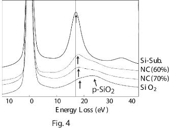
EELS-low loss spectra from the Si substrate, the SiO2 and the Si nanocrystals in samples with 60 and 70 % Si are shown in Figure 5. The maximum in the plasmon energy peak for pure bulk Si and the Si nanocrystals in the 70 and 60 % samples were 17.2 eV, 18.4 eV and 18.8 eV respectively. A 1.2-1.6 eV difference in plasmon energy between pure Si (substrate) and the Si nanocrystals was therefore observed. Previous studies have attributed the difference in plasmon peak energy between nanocrystals with different sizes to quantum confinement and/or changes in the energy band gap Mitome et al. (1992).
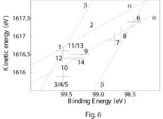
The initial state Auger parameter () was measured using equation 5 and the values are shown in table 3 and plotted in the Wagner diagram in Figure 6, with the values lying on the straight lines with slope +3. The reference valuesMoulde et al. (1992) used in these plots are SiKLL(Si0) = 1616.6 eV, SiKLL(SiO+4) = 1608.8 eV , Si = 103.6 and Si = 99.5. The Wagner diagram (Figure 6) shows a large deviation in between samples with different fractions of Si and heat treatment. Samples containing small, amorphous nanoclusters (e.g. the sample with 28 % Si) have the lowest value for (1912.6 eV), which results in a ( = -) of -2.5 0.4eV, as compared to pure bulk Si. As grown samples and samples with nanocrystals have the largest values, 1915.7 eV ( is -0.7 0.4 eV) and 1914.6 0.3 eV ( of -0.5 eV, for sample with 70 % silicon) respectively . Changes in are a measure of the ground state chemistry, changes in environmental potential and charge transfer Paul et al. (2006). More specifically, negative value is associated with a negative shift of the potential (V) Evans et al. (1992); Moretti (1998). In the above context, the decrease in initial state Auger parameter () of the amorphous nanoclusters indicates an increased accumulation of negative charge as compared to the crystalline nanoclusters.
| Nr. in | area % | -Si | -Si | ||
|---|---|---|---|---|---|
| Wagner | Si | 0.1 eV | 0.1 eV | 0.3 eV | 0.4 eV |
| diagram | |||||
| 1 | 100111Reference samplePowell and Jablonski (2000) | 1716.1 | 0 | 1915.1 | 0 |
| 2 | 100222Substrate | 1716.2 | 0.1 | 1914.2 | -0.9 |
| 3 | 50 | 1715.4 | -0.7 | 1914.4 | -0.7 |
| 4 | 60 | 1715.4 | -0.7 | 1914.4 | -0.7 |
| 5 | 70 | 1715.4 | -0.1 | 1914.4 | -0.7 |
| 6 | 28 | 1715.8 | -0.3 | 1912.6 | -2.5 |
| 7 | 42 | 1715.6 | -0.5 | 1913.0 | -2.1 |
| 8 | 42 | 1715.7 | -0.4 | 1912.9 | -2.2 |
| 9 | 50 | 1715.7 | -0.4 | 1914.1 | -1.0 |
| 10 | 50 | 1715.7 | -0.4 | 1914.5 | -0.6 |
| 11 | 60 | 1715.8 | -0.3 | 1914.4 | -0.7 |
| 12 | 70 | 1715.8 | -0.3 | 1914.6 | -0.5 |
| 13 | 70 | 1715.8 | -0.3 | 1914.4 | -0.7 |
| 14 | 70 | 1715.7 | -0.4 | 1914.3 | -0.8 |
III.5 Final state effects
Final state effects express properties of the short lived, highly excited core hole states and are related to screening efficiency Lawrence (1971). The final state Auger parameter () provides an estimate of the relaxation/screening energy in the presence of core holes, (see equation 4). A high value indicates higher relaxation energy or improved screening efficiency. Final state Auger parameter values are shown in Table 3 and plotted in the Wagner diagram shown in Figure 6 as lines with slope +1.
The variations in between the different samples are smaller than in . The only significant difference in is between bulk Si (substrate and literature Powell and Jablonski (2000) value of pure Si) and the nanoclusters (Si), as well as between bulk Si (Si) and the silicon in the non annealed samples (Si). Bulk silicon has the highest value (1716.2 0.1 eV) in agreement with the literature value for pure silicon, whilst Si has the lowest Auger parameter (1715.4 0.1 eV). The above results indicate that electronic screening of core holes increases in the order SiSiSi.
IV Discussion
IV.1 Initial state effects
Contrary to , the Auger parameter is not completely independent of energy referencing. Therefore, can be potentially influenced by work function differences. The work function is defined as the work necessary to remove a Fermi-level (EF) electron from the crystal to infinity Weinert and Watson (1984); Wigner and Bardeen (1935). EF is the level at which the electrons and protons are balanced, halfway between the valence and conduction bands in intrinsic semiconductors, and it shifts either towards the conduction band, or towards the valence band depending on doping, n and p type respectively.
Since experiments were performed using the same spectrometer, we assume that the effect of spectrometer work function on binding energy (EB) should be negligible. Therefore it can only be differences in the material work function that may contribute to EB. An increase in energy band gap Eg could shift EF upwards towards the vacuum level, thus reducing the work function (). This would be detectable via an increase in the EK of the electrons, an equivalent reduction in EB and a subsequent increase in the chemical shift. An increase in valence charge could also lift up the EF and therefore reduce .
According to the suggested interpretation, plasmon energies and Auger parameter values provided by EELS and XPS respectively, indicate an increase in valence electron density and/or Eg in the amorphous nanoclusters compared to bulk silicon. Either one or both of the two reasons (increased electron density, larger Eg) lift the EF and subsequently reduce of the nanocrystals, influencing thus (lowering) the Si binding energy and increasing the chemical shift.
Pure silicon (Si0) supersaturated in SiO2 prior to annealing shows exactly the opposite behavior in Si peak shifts, chemical shift and differential charging than the amorphous nanoclusters (see Table 2). Also the initial state Auger parameter of Si0 in SiO2 prior to annealing exhibits only a small negative shif compared to the substrate (see Table 3). This implies that the ground state (Si0) of silicon in SiO2 is “more positively charged” prior to annealing and becomes “more negatively charged” upon annealing during formation of amorphous and crystalline nanoclusters. The positive shift (V) of the atomic potential of Si0 in the as grown samples (compared to Si) may be attributed to the need of Si to share electrons with the more electronegative surrounding oxygen atoms. When surrounded by the less electronegative Si atoms, (Si0 atomic environment in nanocrystals), the electrons are located closer to the Si atom.
IV.2 Final state effects
The increase in band gap would also lead to a reduction in the screening efficiency of the conduction electrons and this will be detected as a decrease in . Small nanocrystals have an increased band gap compared to both bulk silicon and larger nanocrystals Brus (1984); Kanemitsu (1995); Kayanuma (1988), and this is reflected in aquiring lower values Moretti (1990). Amorphous Si has a higher band gap (1.6-1.7 eV Tanenbaum et al. (1997); Chu et al. (1986)) than crystalline Si (1.2 eV). We recall that amorphous nanoclusters also have a larger difference in chemical shift, differential charging and initial state Auger parameter, compared to the nanocrystals and the substrate. The final state Auger parameter shows only small differences between crystalline bulk Si and Si nanoclusters (both crystalline and amorphous), but there is no significant difference between the differently sized amorphous or crystalline nanoclusters, therefore it seems that final state effects influence the Si2p binding energy less than initial state effects (see Table 3). The for silicon in both the as grown and post annealed conditions is lower than that in bulk silicon or reference Si, implying a reduced core hole screening. It is known that screening in Si has a non local character Weightman (1998). Therefore the delocalized nature of electron screening in combination with the non-conducting silicon oxide environment would be expected to influence the screening of core holes in the nanoclusters even in the presence of an increased valence electron density.
V Conclusions
We used the Auger parameter to separate initial and final state effects in the Si shift of Si crystalline and amorphous nanoclusters dispersed in SiO2. The Si position in the nanocrystals relative to Si (chemical shift) is determined by initial state rather than final state effects. The negative charge on the Si0 sites in nanoclusters and the positive on the Si0 sites in the supersaturated (with Si) silica, as indicated by the initial state Auger parameter, dominate on both differential charging and chemical shifts. shows that the electron screening of core holes in Si is superior when Si is clustered and not dispersed in SiO2. The core hole screening of Si in the nanoclusters is inferior to that in bulk Si and this is presumably due to its non local character in Si.
VI Acknowledgement
Financial support by FUNMAT-UiO, the University of Oslo and Kristine Bonnevie’s travelling scholarship is greatfully acknowledged. We are also grateful to the referee for his comments.
References
- Kapetanakis et al. (2000) E. Kapetanakis, P. Normand, D. Tsoukalas, K. Beltsios, J. Stoemenos, S. Zhang, and J. van den Berg, J. Appl. Phys. 77, 3450 (2000).
- Boer et al. (2001) E. A. Boer, M. L. Brongersma, H. A. Atwater, R. C. Flagan, and L. D. Bell, Appl. Phys. Lett. 79, 791 (2001).
- Tiwari et al. (1996a) S. Tiwari, F. Rana, H. Hanafi, A. Hartstein, and E. F. Crabbe, Appl. Phys. Lett. 68, 1377 (1996a).
- Pavesi and Lockwood (2004) L. Pavesi and D. J. Lockwood, Silicon Photonics (Springer-Verlag, 2004).
- Tiwari et al. (1996b) S. Tiwari, F. Rana, H. Hanafi, A. Hartstein, E. F. Crabbe, and K. Chan, Appl. Phys. Lett. 68, 1377 (1996b).
- Han et al. (2002) H. S. Han, S. Y. Seo, and J. H. Shin, Appl. Phys. Lett. 79, 4568 (2002).
- Kik and Polman (2002) P. Kik and A. Polman, J. Appl. Phys. 91, 534 (2002).
- Chen et al. (2004) T. P. Chen, Y. Liu, C. Q. Sun, M. S. Tse, J. H. Hsieh, Q. Y. Fu, Y. C. Liu, , and S. Fung, J. Phys. Chem. B 108, 16609 (2004).
- Karadas et al. (2004) F. Karadas, G. Ertas, and S. Suzer, J. Phys. Chem. B 108, 1515 (2004).
- Lombardo et al. (2004) S. Lombardo, B. D. Salvo, C. G. c, and T. B. d, Microelectron. Eng. 72, 388 (2004).
- Blauwe (2002) J. D. Blauwe, IEEE Transactions on Nanotechnology 1, 72 (2002).
- Iwata and Ishizaka (1996) S. Iwata and A. Ishizaka, J. Appl. Phys. 79, 6653 (1996).
- Eickhoff et al. (2005) T. Eickhoff, V. Medicherla, and W. Drube, J. of Electr. Spectr. And rel. Phenom. 137-140, 85 (2004).
- Sun et al. (2003a) C. Q. Sun, L. K. Pan, Y. Q. Fu, B. K. Tay, and S. Li, J. Phys. Chem. B (Letter) 107, 5113 (2003a).
- Sun et al. (2003b) C. Q. Sun, B. K. Tay, Y. Q. Fu, S. Li, T. P. Chen, H. L. Bai, and E. Y. Jiang, J. Phys. Chem. B (Letter) 107, 411 (2003b).
- Dane et al. (2006) A. Dane, D. K. Demirok, A. Aydinli, and S. Suzer, J. Phys. Chem. B 110, 1137 (2006).
- Evans et al. (1992) J. A. Evans, A. Laine, P. Weighman, J. A. D. Matthew, D. A. Woolf, D. I. Westwood, and R. H. Williams, Phys. Rev. B: Condens. Matter 46, 1513 (1992).
- Mejias et al. (1997) J.A. Mejias, V.M. Jimenez, G. Lassaletta, A. Fernandez, J.P. Espinos, and A.R. Gonzalez-Elipe, J. Phys. Chem. 100, 16255 (1996).
- Wagner (1975) C. D. Wagner, Anal. Chem. 47, 1201 (1975).
- Gaarenstrom and Winograd (1977) S. W. Gaarenstrom and N. Winograd, J. Chem. Phys. 67, 3500 (1977).
- Thomas and Weightman (1986) T. D. Thomas and P. Weightman, Phys. Rev. B: Condens. Matter 33, 5406 (1986).
- Walker et al. (1994) C. G. H. Walker, G. B. S. A. Motron, J. A. D. Matthew, and F. N. Yousif, J. Electron. Spectrosc. Relat. Phenom. 70, 73 (1994).
- Matthew et al. (1995) J. A. D. Matthew, S. A. Morton, C. G. H. Walker, and G. Beamson, J. Phys. D: Appl. Phys. 28, 1702 (1995).
- Moretti (1998) G. Moretti, J. Electron. Spectrosc. Relat. Phenom. 95, 95 (1998).
- Mitome et al. (1992) M. Mitome, Y. Yamazaki, H. Takagi, and T. Nakagiri, J. Appl. Phys. 72, 812 (1992).
- Castle and West (1979) J. E. Castle and R. H. West, J. of Electr. Spectr. And rel. Phenom. 16, 195 (1979).
- Powell and Jablonski (2000) C. J. Powell and A. Jablonski, NIST Electron Inelastic-Mean-Free-Path Database 71 (National Institute of Standards and Technology, 2000).
- (28) http://www.casaxps.com/.
- Thøgersen et al. (2006) A. Thøgersen, S. Diplas, J. Mayandi, A. Gunnes, T. Finstad, M. Mitoome, Y. Bando, and A. Olsen, in preparation.
- Grunthaner. et al. (1987) P. J. Grunthaner., M. H. Hecht, F. J. Grunthaner, and N. M. Johnson, J. Appl. phys. 61, 629 (1987).
- Jirka (1997) I. Jirka, J. Phys. Chem. B 101, 8133 (1997).
- Hirose et al. (2003) K. Hirose, H. Kitahara, and T. Hattori, Phys. rev. B 67, 195313 (2003).
- Smith and Black (1984) K. L. Smith and K. M. Black, J. Vac. Sci. Technol. A. 2, 744 (1984).
- Wagner et al. (1982) C. D. Wagner, D. E. Passoja, H. F. Hillery, T. G. Kinisky, H. A. Six, W. T. Jansen, and J. A. Taylor, J. Vac. Sci. Technol. A. 21, 933 (1982).
- Himpsel et al. (1988) F. J. Himpsel, F. R. McFeely, A. Taleb-Ibrahimi, J. A. Yarmoff, and G. Hollinger, Phys. Rev. B: Condens. Matter 38, 6084 (1988).
- Carrier et al. (2002) P. Carrier, L. J. Lewis, and M. W. C. Dharma-wardana, Phys. Rev. B 65, 165339 (2002).
- Kroll and Schulte (2006) P. Kroll and H. J. Schulte, Phys. stat. sol. 243, R47 (2006).
- Daldosso et al. (2003) N. Daldosso, M. Luppi, S. Ossicini, E. Degoli, R. Magri, G. Dalba, P. Fornasini, R. Grisenti, F. Rocca, L. Pavesi, S. Boninelli, F. Priolo, C. Spinella, F. Iacona, Phys. Rev. B 68, 085327 (2003).
- Anwar et al. (1990) M. Anwar, C. A. Hogarth, and R. Bulpett, J. Mater. Sci. 25, 1784 (1990).
- Moulde et al. (1992) J. F. Moulde, W. F. Stickle, P. E. Sobol, and K. D. Bomben, Handbook of X-Ray Photoelectron Spectroscopy (Perkin-Elmer Corporation, 1992), p. 201.
- Paul et al. (2006) B. S. Paul, W. Andrzej, and F. Hajo, Chem. Phys. Lett. 420, 42 (2006).
- Lawrence (1971) S. C. Lawrence, J. Phys. Chem. 55, 95 (1971).
- Weinert and Watson (1984) M. Weinert and R. E. Watson, Phys. Rev. B 29, 3001 (1984).
- Wigner and Bardeen (1935) E. Wigner and J. Bardeen, Phys. Rev. B 48, 84 (1935).
- Brus (1984) L. E. Brus, J. Chem. Phys. 80, 4403 (1984).
- Kanemitsu (1995) Y. Kanemitsu, Physics reports review section of physics letters 263, 1 (1995).
- Kayanuma (1988) Y. Kayanuma, Phys. Rev. B 38, 9797 (1988).
- Moretti (1990) G. Moretti, J. Electron. Spectrosc. Relat. Phenom. 50, 289 (1990).
- Tanenbaum et al. (1997) D. M. Tanenbaum, A. L. Laracuente, and A. Gallagher, Phys. Rev. B 56, 4243 (1997).
- Chu et al. (1986) T. L. Chu, S. S. Chu, S. T. Ang, D. H. Lo, A. Duong, and C. G. Hwang, J. Appl. Phys. 59, 1319 (1986).
- Weightman (1998) P. Weightman, J. Electron. Spectrosc. Relat. Phenom. 93, 165 (1998).