Compositional disorder and tranport peculiarities in the amorphous indium-oxides
Abstract
We present results of the disorder-induced metal-insulator-transition (MIT) in three-dimensional amorphous indium-oxide films. The amorphous version studied here differs from the one reported earlier [Phys. Rev. B 46, 10917 (1992)] in that it has a much lower carrier concentration. As a measure of the static disorder we use the dimensionless parameter . Thermal annealing is employed as the experimental handle to tune the disorder. On the metallic side of the transition, the low temperature transport exhibits weak-localization and electron-electron correlation effects characteristic of disordered electronic systems. These include a fractional power-law conductivity versus temperature behavior anticipated to occur at the critical regime of the transition. The MIT occurs at a 0.3 for both versions of the amorphous material. However, in contrast with the results obtained on the electron-rich version of this system, no sign of superconductivity is seen down to 0.3K even for the most metallic sample used in the current study. This demonstrates that using as a disorder parameter for the superconductor-insulator-transition (SIT) is an ill defined procedure. A microstructural study of the films, employing high resolution chemical analysis, gives evidence for spatial fluctuations of the stoichiometry. This brings to light that, while the films are amorphous and show excellent uniformity in transport measurements of macroscopic samples, they contain compositional fluctuations that extend over mesoscopic scales. These, in turn, reflect prominent variations of carrier concentrations thus introducing an unusual type of disorder. It is argued that this compositional disorder may be the reason for the apparent violation of the Ioffe-Regel criterion in the two versions of the amorphous indium-oxide. However, more dramatic effects due to this disorder are expected when superconductivity sets in, which are in fact consistent with the prominent transport anomalies observed in the electron-rich version of indium-oxide. The relevance of compositional disorder (or other agents that are effective in spatially modulating the BCS potential) to other systems near their SIT is discussed.
pacs:
72.80.Ng 72.15.Rn 68.55.Ln 68.35.DvI Introduction
The metal-insulator and the superconductor-insulator transitions (MIT and SIT respectively) are two major representatives of quantum phase transitions that have been extensively studied over the last decades. Disorder driven MIT 1 could be affected by a number of means; doping, pressure, stress, etc. 2 ; 3 ; 4 . A unique method to drive the system from the insulating to the metallic (or superconducting) state is feasible in some metallic glasses prepared from the gaseous phase. Amorphous films quench-condensed onto substrates by vacuum deposition usually contain micro-voids and have a lower mass-density than the respective equilibrium material 5 and thus, on average, smaller interatomic overlap. Thermal treatment at pre-crystallization temperatures may then be used to reduce the free volume created by the micro-voids 5 . In this method one controls the inter-atomic overlap in a similar vein as in employing hydrostatic pressure on a solid. The main difference is that thermal annealing inevitably causes an irreversible volume change.
Thermal annealing has been employed to change the resistivity of amorphous indium-oxide films while monitoring their optical properties 6 . Typically, 3-5 orders of magnitude in room temperature resistivity could be obtained accompanying a 3% reduction in sample thickness (measured by x-ray interferometry 6 ), which is a much larger volume change than is commonly achievable by hydrostatic pressure. Using this technique, the SIT in a three-dimensional indium-oxide films was mapped by measuring the low temperature conductivity as function of disorder 7 . The amorphous indium-oxide had electron density of 10cm and the samples static disorder was characterized by (defined in section II). In this version of indium-oxide, superconductivity survived in samples with 0.24, and, somewhat paradoxically (but reconcilable by an inhomogeneous scenario discussed in this paper), insulating behavior sets in at smaller disorder, for 0.3. The observation that both limits are below the Ioffe-Regel criterion motivated us to conduct the present study employing the same technique of tuning disorder and using the same material but with a much smaller carrier concentration. The idea was to see whether the problem is related to the existence of superconducting or to electron-electron (e-e) correlations effects; in either case one expects the results to depend on carrier concentration.
In this work we map the MIT in three dimensional amorphous indium-oxide films with a carrier concentration that is 2-3 orders of magnitude lower than the material used in 7 . No sign of superconductivity is found down to 0.3K, and normal transport properties are observed for both the insulating and metallic regimes. However, the critical disorder, separating the metallic from the insulating regime, still appears to be given by 0.3 as in the electron-rich phase. By comparison, the MIT in the previously studied 8 crystalline version of indium-oxide occurs at 0.75, which led us to examine the structural differences between the two phases that might account for the different at the transition.
We present data on the microstructure of both the electron-rich and the low carrier-concentration versions of amorphous indium oxide using high resolution microscopy and energy-dispersive local probe. Chemical analysis reveals that the indium-oxygen ratio fluctuates across the sample on mesoscopic scales. Combining this information with Rutherford backscattering and Hall effect measurements suggests that large spatial fluctuations of carrier concentration exist in these amorphous samples. The specifics of this inhomogeneity is argued to be a natural cause for a variety of transport anomalies in these as well as in other systems where superconductivity plays a role at experimentally accessible temperatures.
II Samples preparation and measurements techniques
The InxO films used here were e-gun evaporated on room-temperature microscope-slides using 99.999% pure In2O3 sputtering target pieces. Deposition was carried out at the ambience of (2-5)10 Torr oxygen pressure maintained by leaking 99.9% pure O2 through a needle valve into the vacuum chamber (base pressure 10 Torr). Rates of deposition used for the samples reported here were typically 0.18-0.8 Å/s. For this range of rate-to-oxygen-pressure, the InxO samples had carrier-concentration n in the range (5-13)10cm measured by Hall-Effect at room temperature. Electron-rich InxO samples used in the study (with carrier-concentration in the 10cm range) were produced with the conditions described earlier 7 . The films thickness in this study was 900-1500 Å, which makes them effectively three-dimensional (3D) down to the lowest temperature in our experiments (0.3K) for most of the samples used in this work.
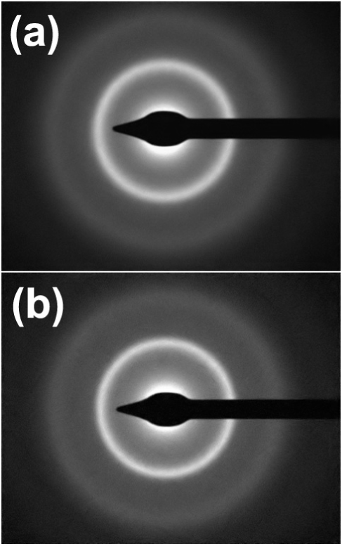
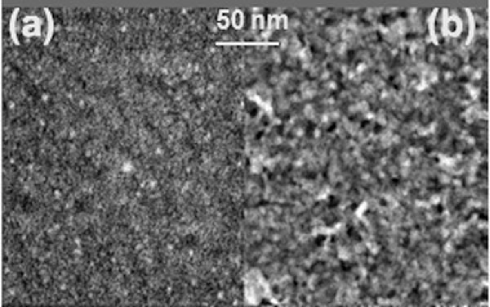
The as-deposited samples had extremely high resistivity of the order of 10-10cm. These were barely measurable even at room temperature. To carry out the low temperatures studies, the samples had to be reduced by several orders of magnitude. This was achieved by thermal annealing. A comprehensive description of the annealing process and the ensuing changes in the material microstructure are described elsewhere 6 ; 9 . For completeness, we give here the basic protocol that was used in this study. Following deposition and initial conductance measurement that, in many cases required the use of electrometer (Keithley 617), the sample was attached to a hot-stage at a constant temperature Ta, initially 5-10 degrees above room temperature. The resistance R of the sample was observed to slowly decrease over time. Tawas raised by few degrees whenever over 24 hours was less than 1% (and the value of the resistance was still higher than desired). To obtain a sample with that was useful for the measurements reported here usually took 20-38 thermal cycles. The annealing temperature Ta was limited to 370 K to minimize the risk of crystallization. The amorphicity of the samples during the annealing process was monitored by checking the diffraction pattern of a controlled specimen prepared on a carbon-coated copper grid. The control specimen was deposited simultaneously with the sample used for the transport measurement but its thickness was limited to 200-300 Å to facilitate high resolution microscopy. Electron-diffraction micrograph of the as-deposited material is shown in Fig. 1a along with a micrograph taken for the same grid after a prolong period of thermal annealing resulting in resistance change of more than three orders of magnitude. Note the characteristic broad rings of the amorphous phase, and in particular the absence of any diffraction ring of either crystalline indium-oxide or metallic indium.
Conductance and Hall Effect measurement were carried out on samples that were patterned in a 6-probe configuration using stainless-steel masks during deposition. We used a standard Hall-bar geometry with the active channel being a strip of either 0.6 mm or 1 mm wide, and 10 mm long. The two pairs of voltage probes (that doubled as Hall-probes), were spaced 3 mm from one another along the strip. This arrangement allowed us to assess the large scale uniformity of the samples, both in terms the longitudinal conductance and the Hall effect. Excellent uniformity was found on these scales; resistivities of samples separated by 1 mm along the strip were identical to within 2% for all the samples used in the study. It should be noted however that microstructural studies performed in the course of the study revealed prominent inhomogeneities on mesoscopic scales (10-10 Å). The effects of these medium-scale irregularities on electronic transport are discussed in the next section.
Most of the conductance versus temperature measurements were done in the 1.3T15K range by a four terminal dc technique using Keithley K220 current-source while monitoring the voltage with Keithley K2000. For lower temperatures measurements (down to 280 mK), we used a four terminal ac technique with the lock-in PAR124A. In all cases care was taken to maintain linear-response conditions by keeping the voltage across the sample low enough. This was verified by measuring the current-voltage characteristics at the lowest temperature of the experiment.
As in previous studies 6 ; 7 ; 8 , we use in this work =(3) as a dimensionless measure of the material disorder. This is based on free-electron expressions using the measured room-temperature conductivity and the carrier-concentration n, obtained from Hall-Effect measurements, as input parameters. More details of preparation and characterization of InxO samples are given elsewhere 6 .
III Results and discussion
One of the main goals of the research was to identify the critical at which the metal-to-insulator transition occurs in the low-n version of InxO. This was accomplished by measuring over a certain range of temperatures, then extrapolate the data to (0) to determine whether the system is insulating (0) or metallic (0. Four different deposition batches were used in this phase of the research. In each of these, thermal annealing was used, in effect, generating samples with different from the same physical specimen. A specific series of for samples labeled by their values is shown in Fig. 2. Note that the plots for samples with 0.4 are nearly parallel to each other, a feature commonly found in many systems on the metallic side of the metal-insulator transition. The usual practice adopted in these cases is to extract the value of by fitting the measured for a given sample to:
| (1) |
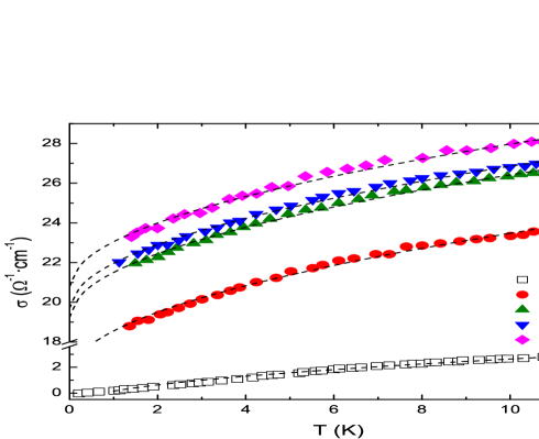
that presumably describes transport corrections to the conductivity due to either weak-localization or e-e interactions effects 1 . Eq. 1 offers a reasonably good fit to the data of samples having 0.4 (Fig. 2).
However, the temperature dependence of the conductance for samples that are in the immediate vicinity of the transition suggests that another law might be relevant, and that should perhaps be taken into account in extrapolating to zero temperature. So, before discussing the versus results we digress now to examine the data, shown in Fig. 3, for samples in the critical regime of the transition.
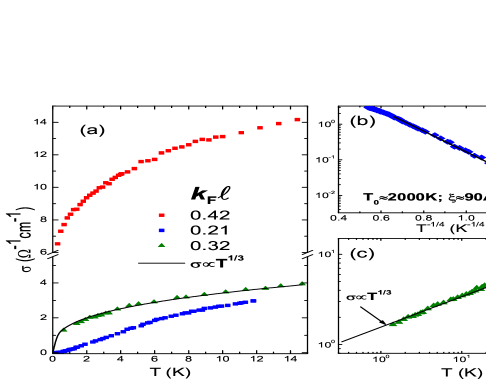
The figure illustrates how the form of changes when the system goes from metallic to insulating behavior (Fig. 3a). The outstanding case is the middle curve that belongs to a sample that is just insulating; it fits well a power-law dependence over a wide range of temperatures as illustrated in Fig. 3c. A temperature dependence of this form is consistent with the interaction effect proposed by Larkin and Khmel’nitskii (LK) 10 . These authors observed that at the transition the contribution of Coulomb interactions to the conductance may be expressed by:
| (2) |
where is the exponent that describes the spatial dependence of the Coulomb potential (with 13). Note that this implies the lack of metallic screening at this range of disorder, heralding the approach of the dielectric phase.
An alternative to the LK mechanism, offered by Imry 11 , has been invoked to account for a component observed in three-dimensional In2O3-x samples near the transition 12 . The Imry mechanism takes account of the scale dependent diffusion that is a property of the critical regime. To obtain the 1/3 exponent, it also assumes a linear-with-temperature electron inelastic-rate . A scattering rate is consistent with the results of our magneto-conductance measurements in the range 4K77K discussed later (Fig. 9).
The conductance component associated with the Imry and the Larkin-Khmel’nitskii mechanism is proportional to and respectively. Here = is the inelastic diffusion-length ( is the diffusion constant that in the critical regime is scale-dependent), and = is the LK interaction-length. The prefactors associated with of these mechanisms are not presently known so we cannot determine their relative contribution. However, for either mechanism, the term should be observed once where is the correlation length 12 and is the relevant scale for the measurement at hand. Therefore, over some temperature range, of metallic samples that are sufficiently close to the transition may be describable by:
| (3) |
where and is the sum of the contributions of the Imry and LK mechanisms.
As may be expected from the similarity between the two functions, the of the (metallic) samples can be fitted to either Eq. 1 and Eq. 3 almost equally well except near the transition where Eq. 3 is a better fit. For the sample with =0.42 (top curve in Fig. 3a), the best fit to Eq. 3 yields a chi-square test value of 0.013 as compared with 0.08 for the best fit to Eq. 1. In general, fitting to Eq. 1 typically gave higher value for the zero-temperature conductivity (the =0.42 sample data gave 6.3cm versus 4.1cm using Eq. 1 and Eq. 3 respectively, a 50% difference). The difference in between the two fitting possibilities however becomes less important for larger , as can be seen in Fig. 4a. For comparison, figure 4a also includes the results of versus for In2O3-x, the crystalline version of 3D indium-oxide.
It is noteworthy that metallic samples with = are obtained in both systems (, calculated by the free-electron expression, is 810cm and 1210cm for the InxO and In2O3-x respectively). Quantum and e-e interaction effects are therefore quite prominent in the low temperature transport properties of these samples.
Data delineating the critical for the transition in the high-n version of InxO are shown in Fig. 4b. This is based on the dependence of the activation energy on for samples that are on the insulating side of the transition (but close to it) 13 . These samples exhibit 7 a peculiar law that empirically has been fitted to simple activation: exp. The critical may be determined in this case by extrapolating to zero 14 .
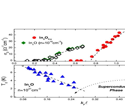
Comparing the data for the three different versions of the material there are two issues that require elucidation; The difference between the various phases in terms of exhibiting superconductivity at the experimentally accessible range, and the difference in the value of at which the metal-insulator transition occurs.
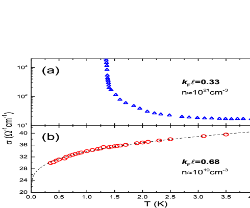
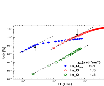
Note that electron-rich InxO samples with 0.3 exhibit superconductivity for 3K (Fig. 4b) while the low-n InxO version shows no sign of superconductivity down to 0.3K even for samples with as high as 0.68 (Fig. 5). It seems plausible that the difference between the high-n InxO, and the low-n version, is the large disparity in their carrier-concentration. Likewise, the low carrier-concentration of In2O3-x (n510cm) is presumably the main reason for the absence of superconductivity in this system 15 . A difference of 2-3 orders of magnitude in carrier concentration is large enough to push down the superconducting transition temperature well below the experimental range; a mere factor of 3 in the BCS potential suffices to shift from 3-4K to less than 10mK.
The important corollary that follows from this observation is this: is not a good parameter to characterize disorder when superconductivity is concerned. Reducing (by e.g., decreasing the carrier concentration), weakens the BCS potential and the superconducting transition temperature will decrease more than by reducing to achieve the same . Increasing the static disorder will reduce but this is not necessarily detrimental to superconductivity. It may actually enhance it 16 . Even in the case that superconductivity is suppressed by disorder it is a weaker effect than the exponential decrease associated with reducing the BCS potential; the latter can easily push the transition temperature to well below experimental reach creating the false appearance of a superconductor to metal transition. may still be a descriptive measure of disorder when care is taken to keep constant in the process of varying the disorder as was done in 7 .
Despite the huge difference in their carrier concentration (more than two orders of magnitude), the MIT in the two InxO versions occurs at essentially the same (see Fig.4). Our conjecture, that the apparent violation of the Ioffe-Regel criterion in the electron-rich InxO is due to correlations, is not supported. The low value of at the transition is therefore more likely related to some properties of the amorphous phase that differ from the crystalline version of the material where the critical is close to unity.
The crystalline and amorphous phases of indium-oxide differ in several aspects (in addition to symmetry). While the crystalline version, in agreement with theoretical considerations 17 , behaves as a nearly free electron system 18 , optical absorption due to interband transition of InxO samples are inconsistent with a parabolic conduction band 6 . Values of estimated for this material by using free-electron formulae may therefore be questionable. Another possibility is that transport in the system is more inhomogeneous than might be judged by the space-filling, physically uniform structure reported for this material 7 ; 19 ; 20 . Note that when the sample resistivity is not uniform, based on macroscopic measurements of conductance and carrier concentration may not be telling of the relevant disorder and the calculated value of may differ from that associated with the ‘average’ disorder. This could be a real problem when the inhomogeneity in the system is so gross as to cause current to flow preferentially through only part of the structure.
In the following we describe how some structural attributes of the amorphous indium-oxides give rise to inhomogeneities in these systems (and possibly in other multi-component systems like alloys and metal-oxides). These may lead to a host of low temperature transport anomalies when superconductivity is involved in addition to an underestimated
The stoichiometric compound In2O3 is an ionic insulator with a large (3.6eV) band gap. It is a well characterized material, has a cubic structure with 48 oxygen atoms and 32 indium atoms in a unit cell. The naturally occurring material however is oxygen deficient, and films of crystalline indium-oxide usually contain 5-10% oxygen vacancies 21 . This gives rise to carrier-concentration n610cm and a factor of 2 around this value may be affected by changing the stoichiometry using, e.g., UV-treatment 22 . The limited range of achievable n is due to constraints imposed by crystal chemistry.
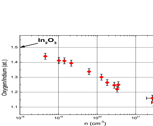
Amorphous indium-oxide, being relatively free of these constraints, may be prepared with a much wider atomic ratio of oxygen-indium. This makes it possible to make stable (more accurately; metastable with a long lifetime at room temperatures and below) films with optical gaps between 2.5eV to 1.1eV and carrier concentration of 510-10 cm respectively 6 . The correlation between stoichiometry and carrier concentration of amorphous indium-oxide is shown in Fig. 6.
The freedom from crystal chemistry constraints is perhaps also the reason for the emergence of compositional-disorder in these amorphous oxides. This kind of spatial disorder has far reaching consequences, especially when superconductivity is involved.
Spatial disorder means that the material parameters vary in space, disordered systems are inhomogeneous by definition.
The nature of the inhomogeneity however, depends on the type of disorder. Quenched disorder of the ionic potential is common in most disordered electronic systems. Large spatial fluctuations of carrier concentration on the other hand are unlikely to occur in systems with mono-atomic metallic systems but they are quite prominent in all versions of the amorphous indium-oxides. Figure 7 is a micrograph taken by a scanning mode of a transmission electron microscope. The contrast mechanism in the micrograph is due to absorption; changing the angle between the sample plane and the electron beam axis does not turn a black region into white (as it often would in a crystalline sample where the main contrast mechanism is Bragg scattering). There are no holes in the film and thickness variations are relatively small; AFM line scans show 5-20 Å surface roughness for 200 Å films deposited on glass substrates (the smaller value obtained for the low-n version of the material). Chemical analysis, using energy dispersive x-ray spectroscopy and electron energy-loss spectroscopy (EELS) revealed that regions with higher transmission (white patches in the figure) are richer in oxygen, poorer in indium content, and vice-versa for the black regions. Variations in the O-In ratio between these regions could be as high as 15-40% for a sampling area of (50 Å). The uncertainty in these measurements is mainly due to the background signal from the carbon support that includes a certain amount of oxygen. This source of error may be mitigated by making self-supporting films but a systematic study of thickness dependence will be necessary to get a more accurate estimate of stoichiometry. Note however, that a mere 10% variation in O-In ratio is equivalent to an order of magnitude difference in the local carrier-concentration (c.f., Fig. 6), which is tantamount to a factor of two in the thermodynamic density of states.
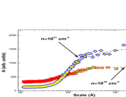
The spatial range of these compositional fluctuations can be assessed by Fourier transforming line scans of the intensity, averaged over the entire micrograph area (only a part of which is shown in Fig. 7). Results of such analyses, done for the two InxO samples of Fig. 7, are shown in Fig. 8. The flattening out of the spectrum at the small spatial scales is partly due to the smoothing effect of oxygen-diffusion and partly due to the STEM resolution. Note that the low-n InxO is somewhat more uniform than the high-n version. However, in both cases the spectrum is skewed in a similar way and the compositional fluctuations persist over scales extending up to 300-800 Å.
These scales are comparable or even larger than the length scales that may be relevant for transport; (and , the superconducting coherence-length). Pertinent information on these transport parameters may be obtained by analyzing magneto-conductance (MC) data. We have measured ten InxO metallic samples at 4K, and for comparison, also at 77K. At small fields the MC for all metallic samples was positive and that remained so down to 2K (tested on one of these samples). Spin orbit scattering in InxO is therefore rather limited in strength. A negative MC component however does appear at high fields as seen in the data described in figure 9.
Figure 9 compares the MC of our most metallic InxO sample with a In2O3-x sample of comparable resistivity. The latter system has been extensively studied and exhibits of 1000-1300 Å at 4K for samples with of order 2-5 23 . The field at which the MC crosses over from H to a weaker dependence is 25 times larger for the InxO sample. This suggests a considerably smaller than that of In2O3-x at the same temperature. We have analyzed the low field MC for the amorphous sample using Kawabata’s 24 expression: = in conjunction with the Drude expression for the conductivity = using m*0.28(mass of the free electron). This yielded the parameters: 610s, 12 Å (using 210cm/s), (at 4.1K)=45020 Å, 2 cm/s. The interaction length is then 70 Å and 140 Å depending on whether = or respectively. At temperatures relevant for our experiments these length scales are not large enough to average out the compositional inhomogeneities observed in these materials.
Although it may have no direct bearing on the main issues of this work, it is important to point out that the MC of the InxO samples differs from the MC in the crystalline version by more than the magnitude of . The negative MC component of the metallic sample in Fig. 9, that is just observable above 6.5T, becomes quite noticeable at lower temperatures (but down to 1.4K it is only seen above 3T). The MC in diffusive In2O3-x samples is purely positive, throughout the entire range up to fields of 12T and down in temperature from 77K to 40mK. There is also a difference between InxO and the crystalline In2O3-x version in terms of the MC for insulating samples; The MC in insulating In2O3-x starts positive and becomes negative at high fields 25 while just the opposite is observed in our insulating InxO sample (with =0.23) for temperatures below 3K.
Results of MC measurements on InxO films were reported by Lee et al 26 . Their results differed from ours; they observed positive MC only above 8-10K while the low field MC became negative at lower temperatures. It should be noted however that the InxO films of Lee et al were presumably the electron-rich version (and exhibited superconductivity for 1K when the resistance was low enough). More work is needed to identify the origin of the mechanism that is responsible for the negative MC at both the metallic and insulating regime of the different versions of InxO.
Fluctuations in carrier concentrations on the spatial scales observed in the amorphous indium-oxides constitute an important type of disorder. Screening is more effective in regions with larger n, which means that the conductance in these regions is higher (although the mobility may be impaired in these regions, partially offsetting this effect). When the sample resistivity is not uniform, based on macroscopic measurements of conductance and carrier concentration will in general be underestimated; since current naturally flows preferentially through the more conducting regions of the structure, the ”active” volume for transport is smaller than that assumed by its geometric dimensions. The non-uniform current distribution affects the perceived values of both, the conductivity and the carrier-concentration which are used in assigning a value of to a given sample. This is based on =(3) and therefore errors in have a lesser effect than errors in unless the system inhomogeneity is excessive (the Hall voltage may be significantly suppressed in e.g., filamentary conduction yielding a spuriously huge ). It seems intuitively plausible that, in general, inhomogeneity causes to be underestimated while the Hall-derived is if anything somewhat overestimated. These consideration may explain why the metal to insulator transition in the two versions of InxO occurs for that is smaller than unity. At the same time, for scales of the order of millimeters, these compositional inhomogeneities are well-averaged, and therefore the excellent uniformity of the InxO films mentioned in section II is not at variance with the observed mesoscale inhomogeneity.
A more profound modification of transport should occur at low temperatures when superconductivity appears. This is where the value of as a parameter that characterizes disorder has questionable merit; carrier-rich regions of the system are more likely to go superconducting than regions where n is small. As demonstrated in Fig. 5, the sample with the larger carrier concentration goes superconducting despite having a smaller than a sample with a larger mean-free-path. It is the BCS potential that plays the crucial role in these situations, and when its local value fluctuates in the system on scales that are comparable or larger than , inhomogeneity is dramatically enhanced. In this case the system breaks into a ‘granular-like’ structure; islands of zero resistance precipitate in a normal matrix. The latter may be either metallic or insulating depending on the (average) degree of disorder, carrier concentration, and temperature. Due to proximity and Josephson effects (that are temperature dependent), the scales of the superconducting islands and their spatial distribution may somewhat differ from those set by the compositional disorder.
The following transport anomalies found in the electron-rich version of InxO are in line with this picture:
1) The critical disorder for the SIT is scale dependent; short samples may go superconducting while longer ones, made on the same strip and having essentially the same (normal state) resistivity, exhibit insulating behavior 20 .
2) On the just insulating side of the transition, where the conductance versus temperature follows exp, the activation energy increases monotonously with the sample length 20 .
3) The current voltage characteristics of these samples revealed discontinuous jumps similar to those found in Josephson arrays 19 .
4) A non-monotonous MC is observable in InxO films near their SIT; The conductance first decreases with field reaching, in some cases, a much smaller value then its asymptotic value at high fields 27 .
Significantly, all these anomalies appear at the temperature range where the less disordered material is superconducting.
Other possible manifestations of superconducting islands coexisting with normal regions were obtained in 28 and in recent tunneling experiments from large area electrodes into InxO films in the insulating regime 29 . It may be difficult to observe these non-superconducting regions by a scanning tunneling technique (STM) due to the spreading resistance associated with resistive paths but the inhomogeneous nature of superconductivity has been seen by STM in InxO films 30 (and in TiN 31 ).
The observation that the InxO films are structurally continuous, and being amorphous, free of grain boundaries etc., was an inducement to offer an inherent ‘disorder induced granularity’ scenario for these phenomena 19 ; 20 . The effects associated with this scenario ought to have been apparent in all materials near their SIT provided that superconductivity is not suppressed by disorder before a ‘critical ’ is reached 19 ; 20 . Several systems such as TiN 32 and NbN 33 indeed exhibited some of these transport anomalies near their SIT (specifically, a non-monotonous MC). However, the magnitude of these effects were not as prominent as they are in the electron-rich InxO samples. Moreover, these peculiarities are not usually observed near the disorder-tuned 34 SIT of amorphous Bi and Pb films, except when structural granularity was deliberately introduced to modify their microstructure 35 .
We have therefore to conclude that, while the ‘inherent disorder-induced’ inhomogeneity is a plausible physical scenario, it appears that the modulation-depth of local superconducting properties caused by potential fluctuations is much less conspicuous than that of fluctuations in carrier-density. In other words, the type of disorder is an important ingredient in producing prominent ‘granularity effects’ near the SIT. Unless they break time-reversal symmetry, potential fluctuation have a mild effect on (which can be of either sign 16 ). Spatial fluctuation in the BCS potential, on the other hand, is a powerful agent for local modulation of , and it may facilitate the two-phase state responsible to the observed transport peculiarities. An effective way to achieve it is by modulating carrier concentration, which seem to occur naturally in the amorphous indium-oxides.
This type of disorder is energetically unfavorable in a mono-atomic system like amorphous Bi unless the system is physically discontinuous. On the other hand, in an alloy or metal oxide, compositional-disorder may compensate for the carrier concentration difference by a chemical one without compromising the physical continuity of the structure. Grain boundaries and other extended defects may also play a role in creating inhomogeneous BCS potential distribution when pair-breakers such as magnetic impurities (that tend to segregate at these defects) are present in the system.
The corollary that emerges from these considerations is that while disorder is tantamount to inhomogeneity, the degree and detailed nature of the resulting spatial fluctuation depend on the type of disorder, not just on its magnitude. This distinction may be less important for the non-interacting system but it is crucial for the subtle case of superconductivity.
One of the questions raised in the study of insulating InxO films near the SIT 7 was the origin of the dependence of the conductance on temperature exp. An arrhenius law for is intriguing in that it occurs in a disordered system for which the natural choice is the variable-range-hopping (VRH) mechanism 5 , which indeed is exhibited by just-insulating samples of the low-n version of InxO (Fig. 3b). The study reported in 7 used a three-dimensional system. The activation energy of the insulating samples increased monotonously with disorder reaching a mximum of 7K before the conduction mechanism reverted to variable range hopping 7 . It was shown in a subsequent study using a two-dimensional version of this system that may reach 14-15K 19 for a similar range of used in the 3D system. The dimensionality and length dependence of are characteristic signs of a percolative phenomenon.
These observations suggest that the origin of the exp or a somewhat faster dependence 19 , is the appearance of superconducting islands in an insulating medium. In the insulating regime of the SIT (and at temperatures where the material is fully in the normal state), most of the electron-rich areas are weakly coupled to other regions, say with typical coefficient 1. As the temperature falls below the local of these regions, the coupling (being now controlled by Andreev processes), becomes 1. Superconducting islands that were part of the current-carrying-network (CCN) in the normal state, will be effectively removed from it thereby forcing a new and less conductive CCN. Transport in the VRH regime takes place in a tenuous current-carrying-network that, for a given disorder, becomes more rarefied as temperature is lowered. An exponential reduction of the conductance occurs when part of the sample volume is eliminated from the transport 36 , a role that the superconducting islands may effectively take.
The range of disorder where this mechanism is relevant is limited to the vicinity of the transition; For sufficiently strong disorder the localization length will be everywhere smaller than and there will be no superconducting islands in the system. In this case the transport mechanism will revert to normal VRH as seen in the experiment 7 . At small disorder, on the other hand, many of the superconducting islands may be Josephson-coupled to form large superconducting clusters. Effective Josephson coupling through insulating InxO layers has been observed experimentally 37 . Global superconductivity may result in the system with the associated percolative features discussed in reference 20 . In this picture is a non-trivial result of hopping conductivity modulated by the compounded effect of the temperature-dependent appearance of superconducting islands and the evolution with temperature of their local pair-potential. In view of the transport features described above this seems to be a prime avenue to look for a solution to this problem.
This work greatly benefitted from an extensive exchange of data and ideas with the research groups of Allen Goldman, and Aviad Frydman. We also acknowledge illuminating discussion with O. Agam, D. Khmel’nitskii, Y. Imry, and M. Feigel’man. One of us (Z.O.) expresses his gratitude to F. P. Milliken for help in getting some of the Rutherford Backscattering data at the IBM research Center, Yorktown-Heights. This research has been supported by the Binational US-Israel Science Foundation and by The Israeli Academy for Sciences and Humanities.
References
- (1) W. L. McMillan, Phys. Rev. B 24, 2739 (1981); Patrick A. Lee and T. V. Ramakrishnan, Rev. Mod. Phys. 57, 287 (1985).
- (2) M. A. Paalanen, T. F. Rosenbaum, G. A. Thomas, and R. N. Bhatt, Phys. Rev. Lett. 48, 1284 (1982); T. F. Rosenbaum, R. F. Milligan, M. A. Paalanen, G. A. Thomas, and R. N. Bhatt and W. Lin, Phys. Rev. B 27, 7509 (1983).
- (3) C. Sekine, T. Uchiumi, I. Shirotani, and T. Yagi, Phys. Rev. Lett. 79, 3218 (1997).
- (4) V. Laukhin, J. Fontcuberta, J. L. García-Muñoz, and X. Obradors, Phys. Rev. B 56, R10009 (1997).
- (5) N. F. Mott and A. E. Davis, electronic Processes in Non-Crystalline Materials, (Oxford University) (1971).
- (6) Z. Ovadyahu, Phys. Rev B 47, 6161 (1993).
- (7) D. Shahar and Z. Ovadyahu, Phys. Rev. B 46, 10917 (1992).
- (8) E. Tousson, E. P. Rubenstein, R. Rosenbaum, V. Volterra and Z. Ovadyahu, Phil. Mag B 56, 875 (1987); E. Tousson and Z. Ovadyahu, Phys. Rev. B 38, 12290 (1988).
- (9) Z. Ovadyahu, J. Phys. C: Solid State Phys., 19, 5187 (1986).
- (10) A. I. Larkin and D. E. Khmel’nitskii, Sov. Phys. JETP 56, 647 (1982); Zh. Eksp. Teor. Fiz. 83, 1140 (1982).
- (11) Y. Imry, J. Appl. Phys. 52 1817 (1981).
- (12) Y. Imry and Z. Ovadyahu, J. Phys. C 15, L327 (1982).
- (13) Samples with 0.25 in this electron-rich version of InxO are superconducting at liquid-helium temperatures and therefore the critical cannot be determined by the low-temperature method used for the non-superconducting In2O3-xand the low-n version of InxO.
- (14) M. V. Feigel’man, L. B. Ioffe, V. E. Kravtsov, and E. A. Yuzbashyan, Phys. Rev. Lett. 98, 027001 (2007).
- (15) Crystalline indium-oxide films were measured down to 12 mK showing no sign of superconductivity, F. P. Milliken and Z. Ovadyahu (unpublished).
- (16) K. Knorr and N. Barth, Solid State Comm., 8, 1085 (1970); E. Babić, R. Krsnik, B. Leontić, and I. Zorić, Phys. Rev. B 2, 3580 (1970); B. Stritzker and H. Wühl, Z. Physik B 24, 367 (1976) and references therein; M. S. Osofsky, R. J. Soulen, Jr., J. H. Claassen, G. Trotter, H. Kim, and J. S. Horwitz, Phys. Rev. Lett. 87, 197004 (2001) and references therein.
- (17) O. N. Mryasov and A. J. Freeman, Phys. Rev. B 64, 233111 (2001).
- (18) O. Cohen and Z. Ovadyahu, Phys. Rev. B 50, 10442 (1994).
- (19) D. Kowal and Z. Ovadyahu, Solid State Comm., 90, 783 (1994).
- (20) D. Kowal and Z. Ovadyahu, Physica C, 468, 322 (2008).
- (21) Z. Ovadyahu, B. Ovryn and H.W. Kraner, J. Elect. Chem. Soc., 130, 917 (1983).
- (22) Z. Ovadyahu, J. Phys. C: Solid State Phys., 19, 5187 (1986).
- (23) Z. Ovadyahu, Y. Gefen and Y. Imry, Phys. Rev. B 32, 781 (1985) and references therein.
- (24) A. Kawabata, Solid State Comm., 34, 431 (1980).
- (25) A. Vaknin, A. Frydman, Z. Ovadyahu, and M. Pollak, Phys. Rev. B 54, 13604 (1996).
- (26) Y. J. Lee, Y. S. Kim and H. K. Shin, J. Phys.: Condens. Matter 14 483 (2002).
- (27) V. Gantmakher, International Journal of Modern Physics B, 12, Nos. 29, 30 & 31 (1998); G. Sambandamurthy, L. W. Engel, A. Johansson, and D. Shahar, Phys. Rev. Lett. 92, 107005 (2004); M. A. Steiner, G. Boebinger, and A. Kapitulnik, Phys. Rev. Lett. 94, 107008 (2005).; T. I. Baturina, A. Bilušić, A.Yu. Mironov, V. M. Vinokur, M. R. Baklanov, and C. Strunk, Physica C 468, 316 (2008).
- (28) S. Poran, E. Shimshoni, and A. Frydman, Phys. Rev. B 84, 014529 (2011).
- (29) D. Sherman, G. Kopnov, D. Shahar, and A. Frydman, Phys. Rev. Lett. 108, 177006 (2012).
- (30) Benjamin Sacépé, Thomas Dubouchet, Claude Chapelier, Marc Sanquer, Maoz Ovadia, Dan Shahar, Mikhail Feigel’man and Lev Ioffe, Nature Physics, 7, 239 (2011).
- (31) C. Chapelier, W. Escoffier, B. Sacépé, J.C. Villégier, and M. Sanquer, AIP Conf. Proc. 850, 975 (2005).
- (32) T. I. Baturina, A.Yu. Mironov, V. M. Vinokur, M. R. Baklanov, and C. Strunk, Phys. Rev. Lett., 99, 257003 (2007).
- (33) Madhavi Chand, Garima Saraswat, Anand Kamlapure, Mintu Mondal, Sanjeev Kumar, John Jesudasan, Vivas Bagwe, Lara Benfatto, Vikram Tripathi, and Pratap Raychaudhuri, Phys. Rev. B 85, 014508 (2012).
- (34) Signs of emergent granularity were observed in the magnetic-field tuned superconductor to insulator transition of thin layers of a-Pb by: J. S. Parker, D. E. Read, A. Kumar and P. Xiong, EPL 75, 950 (2006).
- (35) M. D. Stewart Jr., Aijun Yin, J. M. Xu, James M. Valles Jr., Science 318, 1273 (2007).
- (36) B.I. Shklovskii & A.L. Efros, in: Electronic Properties of Doped Semiconductors, Springer-Verlag (1984); A. Frydman, O. Cohen and Z. Ovadyahu, Solid State Comm., 83, 249 (1992).
- (37) A. Vaknin, A. Frydman, and Z. Ovadyahu, Phys. Rev. B 61, 13037 (2000) and references therein.