Negative photoconductance in SiO2(Co)/GaAs heterostructure in the avalanche regime
Abstract
In the avalanche regime we observed the negative photoconductance of heterostructures of silicon dioxide films containing cobalt nanoparticles grown on gallium arsenide, SiO2(Co)/GaAs. Light irradiation with the photon energy less than the bandgap energy of the GaAs creates holes trapped on defects within the GaAs bandgap, suppresses the avalanche feedback and causes a reduction of the current flowing in the SiO2(Co)/GaAs.
Devices based on avalanche processes such as avalanche photodetectors, photomultipliers, avalanche transistors are critical components in high-speed communication systems, optical radars, quantum cryptography, quantum computing, infrared imaging, laser ranging Gisin02 ; Prev07 ; Voll10 ; Nak2000 . Due to the inherent positive feedback mechanism involved in the impact ionization avalanche process Sze , these devices have high photosensitivity and the ability to switch very high currents with less than a nanosecond rise and fall times. Single-photon detection is one of the most challenging goals of photonics. This goal can be achieved by use of detectors working in the avalanche regime. Single-photon avalanche detectors with self-quenching Zhao07 ; Jiang12 show great suppression in excess noise. Avalanche photodetectors with negative resistance characteristics exhibits the internal radio-frequency-gain effect – the enhanced response in microwave frequencies Kim03 ; Kang07 . Another goal of the avalanche devices such as avalanche transistors and impact avalanche transit time (IMPATT) devices is generation of ultra-narrow pulses and high power signals in microwave, millimeter-wave and terahertz frequencies Vain10 ; Ach12 . Thus, one can conclude that investigation of the avalanche process and manipulation of the impact ionization is very important for various applications.
In this Letter we study influence of light irradiation on the avalanche in (SiO2)40Co60/GaAs heterostructures and observe the negative photoconductance in the infrared region – the current flowing in the heterostructure decreases under the light irradiation. One needs to note that the negative photoeffect can be observed not only on systems with avalanche process, but on semiconductor structures with quantum wells Tut89 ; Cheng94 ; Yak2000 and in films with metal nanoparticles coated by self-assembled monolayers Nak09 . In the first case, the effect is due to the electron confinement in well regions. In the second case, the effect is caused by light-induced creation of mobile charge carriers whose transport is inhibited by carrier trapping in transient polaron-like states. Investigation of SiO2(Co)/GaAs heterostructures is important because the extremely large magnetoresistance ( %) is observed in these structures at the avalanche regime at room temperature Lut05 ; Lut09 .
Experiment. Experiments were performed on metal-dielectric heterostructures composed of thin film of amorphous silicon dioxide with cobalt nanoparticles deposited on gallium arsenide substrates (SiO2)100-xCox/GaAs [the abridge notation is SiO2(Co)/GaAs]. -GaAs substrates with thickness of 0.4 mm are of the (001)-orientation type. Electrical resistivity of GaAs chips was equal to 0.93 cm. Prior to the deposition process, substrates were polished by a low-energy oxygen ion beam Stog02 ; Stog03 . The roughness height of the polished surfaces was less than 0.5 nm. The SiO2(Co) films were prepared by the ion-beam deposition technique using a composite cobalt-quartz target onto GaAs substrates heated to 200∘C. The Co concentration in SiO2 matrix was specified by a relation of cobalt and quartz surface areas. The film composition was determined by the nuclear physical methods of element analysis using a deuteron beam. The cobalt to silicon atomic ratio was measured by the Rutherford backscattering spectrometry of deuterons. The oxygen concentration in films was determined by the method of nuclear reaction with deuterons at = 0.9 MeV: 16O O. This technique is described in more detail elsewhere Zvon . For the samples studied, the relative content of cobalt is equal to 60 at.% and the film thickness is 40 nm. The average size of Co particles was determined by the small-angle X-ray scattering and is equal to 3.5 nm. Protective Au layer of a thickness 3-5 nm have been sputtered on SiO2(Co) films. The Au layer was used as a contact in experiments.
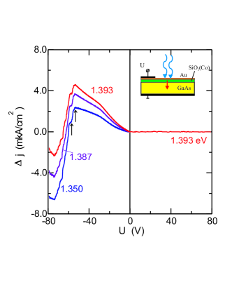
In order to measure the the current change we use the lock-in technique with modulation of light beam at the frequency 40 Hz. Fig. 1 shows the current change caused by the linear-polarized light irradiation with photon energy 1.350 eV, 1.387 eV and 1.393 eV versus the voltage applied on the SiO2(Co)/GaAs heterostructure at room temperature. One contact was on the GaAs substrate, and the other (Au contact) – on the SiO2(Co) granular film. The light intensity is equal to 2.6 mW/cm2. Photon energies are less than the GaAs bandgap energy , the depth of penetration of light into GaAs is high and the light reaches the region of the avalanche process in the GaAs. The dependencies have different character at positive and negative voltages applied to the SiO2(Co) film. At positive voltages no changes in the current is observed. At small values of negative voltages the current change increases. The avalanche process starts at 54 V and the photocurrent begins to decrease. At higher voltages ( 60 ) the light irradiation leads to the suppression of the avalanche process and the becomes negative. At voltages 54 V and 58 V the step-like dependence caused by current filaments is observed Ker82 .
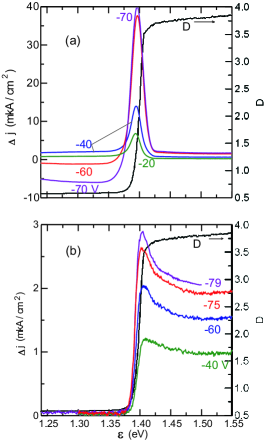
Spectral dependencies of the current change under the light irradiation are presented in Fig. 2(a). At low negative voltages applied on the SiO2(Co) film ( -20, -40 V) the grows and the positive photoeffect is observed. The highest growth of the exists in the narrow band of photon energies 1.38 - 1.41 eV near the bandgap energy of the GaAs. Outside of this band the growth of the is small. At the avalanche process in the GaAs (negative voltages, 54 V) in the energy band 1.38 - 1.41 eV the photocurrent retains its growth with voltage increasing. At the same time, at photon energies 1.38 eV the decrease of the current flowing in the heterostructure is observed and at 54 V the current change . For 1.41 eV one can observe sharp decrease of the , but the photocurrent retains positive values. Fig. 2(b) shows spectral dependencies of the under the light irradiation of the GaAs without a SiO2(Co) film at negative voltages on the GaAs. The light intensity is equal to 0.3 mW/cm2. In contrast to SiO2(Co)/GaAs heterostructures, in the GaAs without a SiO2(Co) film at photon energies 1.38 eV the negative photoeffect is absent and at photon energies 1.41 eV spectral dependencies of the current change do not have the sharp decrease observed on SiO2(Co)/GaAs heterostructures [Fig. 2(a)]. We note that maxima of in Fig. 2(a) are shifted to lower energies in comparison to maxima of in Fig. 2(b).
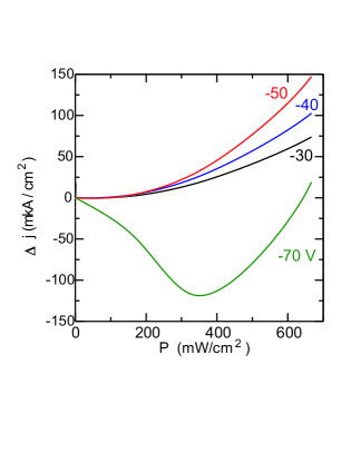
The photocurrent depends on the light intensity (Fig. 3). Without an avalanche in the heterostructure (negative voltages, 54 V), the grows with light intensity increasing. In the avalanche regime ( 70 V), the photocurrent changes its sign and the dependence versus has nonlinear character.
Discussion. Since the interface region of the GaAs contains oxygen ions leaved after the polished process, then according to Lin76 ; Yu84 in addition to the EL2 defect level there are oxygen-ion levels in the GaAs bandgap. The four-level model [Fig. 4(a)] describes the presence of these levels in the GaAs Lin76 . The temperature dependence of dark conductivity near room temperature is controlled by the thermal excitation of electrons from level 1 which lies 0.48 eV below the conduction band. The value of corresponds to the activation energy 0.47 eV of the SiO2(Co)/GaAs structure Lut05 . In thermal equilibrium other three levels 0.74 eV, 1.0 eV and 1.25 eV are mostly occupied.
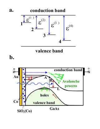
The schematic band diagram of the action of light irradiation on the avalanche process and on the feedback in SiO2(Co)/GaAs heterostructures is shown in [Fig. 4(b)]. The spin-dependent potential barrier is formed in the accumulation electron layer in the semiconductor near the interface (point A) Lut09 ; Lut06a . The impact ionization induced by injected electrons produces holes, which move and are accumulated in the region of the potential barrier. Existence of holes in the region of the barrier lowers the barrier height, grows the electron current flowing through the barrier and leads to the enhancement of the avalanche process. Due to the formed positive feedback small variations in the barrier height give great changes in the current. Light irradiation of heterostructure leads to a creation of free electrons in a conduction band and holes in a valence band, as well as localized electrons and holes on defects inside bandgap of GaAs.
To describe photoinduced processes let us consider the current change caused by light in the avalanche regime. Without a light irradiation the current flowing in a semiconductor structure, where the impact ionization process is formed, is the sum of electron and hole currents, , where is the positive feedback produced by holes. Influence of the light irradiation on the current density flowing in a semiconductor structure can be written as
| (1) |
where is the electron current density in a conduction band induced by the light irradiation, is the light intensity, is the photon energy, and is the function of and . The change in the current density caused by light is determined by the difference between the current density under the light irradiation of the intensity and the current density without an irradiation
| (2) |
Due to the positive feedback the current change can be negative, i.e. negative photoeffect is observed, and can be positive (). Taking into account Eqs. (1) and (2), we find that the negative photoeffect is realized, when the feedback contribution to the current decrease is greater than the contribution to the current increase caused by the electron creation in the conduction band and the inequality
| (3) |
fulfills.
The suppression of the avalanche process presented in Fig. 1 can be explained in the following way. If the photon energy is less than the bandgap energy , , light irradiation causes a creation of conduction electrons in the conduction band and holes trapped on defects within the bandgap of GaAs (Fig. 4). Localized holes on the levels form the region of immovable positive charge. This region hinders the movement of holes, which create in the avalanche process in the valence band and move to the potential barrier. Consequently, the positive feedback decreases. If the value of is high to fulfill relation (3), the current change becomes negative.
For 1.38 eV (Fig. 2) the avalanche process is suppressed, the value of the positive feedback decreases and the photocurrent becomes negative. For 1.41 eV one can observe sharp decrease of the , but the photocurrent retains positive values. This decrease is due to the quantum well formed near the interface [Fig. 4(b)]. Electrons which are created by light irradiation of the SiO2(Co)/GaAs heterostructure are localized in the quantum well. Since electron-hole pairs are created and accumulate in the interface region, the light penetration depth in the GaAs has low values and the light irradiation influence on the positive feedback of the avalanche process is insignificant. This leads to low values of the .
The developed model of the current change caused by light in the avalanche regime can explain the dependence of the photocurrent on the light intensity (Fig. 3). Without an avalanche process ( 54 V) at photon energies lesser than the bandgap energy of the GaAs the light irradiation causes a creation of conduction electrons in the conduction band and holes trapped on defects within the bandgap. In this case, and the photocurrent is determined by the current of activated electrons (Eq. 1). In the avalanche regime ( 70 V) at small values of for the case of fulfilment inequality (3) the feedback contribution to the current decrease is of great values and the current change is negative. At high values of the feedback is suppressed and the grows.
In summary, the negative photoconductance is observed in SiO2(Co)/GaAs heterostructures in the avalanche regime, when the photon energy is less than the energy bandgap of the GaAs. The light irradiation creates holes trapped on defects within the GaAs bandgap. These localized holes hinder the movement of holes created in the impact ionization process in the valence band and reduce the avalanche positive feedback. This leads to the observed decrease of the photocurrent. Thus, in the avalanche regime SiO2(Co)/GaAs heterostructures demonstrate not only the extremely large magnetoresistance, but also the negative photoeffect, which can be used in sensitive infrared detectors.
The authors gratefully acknowledge the assistance of V.M. Lebedev (PNPI, Gatchina, Leningrad region, Russia) for determination of the film composition and R.V. Pisarev and A.M. Kalashnikova for useful discussions. This work was supported by the Russian Foundation for Basic Research (Project Nos. 10-02-01008, 10-02-00516, 10-02-90023), the RAS Programs on Spintronics and Nanostructures, the Ministry of Education and Science of the Russian Federation (project 2011-1.3-513-067-006).
e-mail: l_lutsev@mail.ru
References
- (1) N. Gisin, G. Ribordy, W. Tittel, and H. Zbinden, Rev. Mod. Phys. 74, 145 (2002).
- (2) R. Prevedel, Ph. Walther, F. Tiefenbacher, P. Böhi, R. Kaltenbaek, Th. Jennewein, and A. Zeilinger, Nature 445, 65 (2007).
- (3) M. Vollmer and K.-P. Möllmann, Infrared Thermal Imaging: Fundamentals, Research and Applications, (Wiley-VCH, Weinheim, 2010).
- (4) T. Nakata, T. Takeuchi, I. Watanabe, K. Makita, and T. Torikai, Electron. Lett. 36, 2033 (2000).
- (5) S. M. Sze, Physics of Semiconductor Devices, 2nd ed. (Wiley, New York, 1981).
- (6) K. Zhao, A. Zhang, Yu-hwa Lo, and W. Farr, Appl. Phys. Lett. 91, 081107 (2007).
- (7) X. Jiang, M.A. Itzler, K. O’Donnell, M. Entwistle, and K. Slomkowski, Proc. of SPIE 8375, 83750U (2012).
- (8) G. Kim, I.G. Kim, J.H. Baek, and O.K. Kwon, Appl. Phys. Lett. 83, 1249 (2003).
- (9) H.-S. Kang, M.-J. Lee, and W.-Y. Choi, Appl. Phys. Lett. 90, 151118 (2007).
- (10) S. Vainshtein, V. Yuferev, J. Kostamovaara, and V. Palankovki, Annual Journal of Electronics, 12 (2010).
- (11) A. Acharyya and J.P. Banerjee, Terahertz Science and Technology 5, 97 (2012).
- (12) G. Tuttle, H. Kroemer, and J.H. English, J. Appl. Phys. 65, 5329 (1989).
- (13) J.-P. Cheng, I. Lo, and W.C. Mitchell, J. Appl. Phys. 76, 667 (1994).
- (14) A.I. Yakimov, A.V. Dvurechenskii, A.I. Nikiforov, O.P. Pchelyakov, and A.V. Nenashev, Phys. Rev. B62, R16283 (2000).
- (15) H. Nakanishi, K.J.M. Bishop , B. Kowalczyk, A. Nitzan, E.A. Weiss, K.V. Tretiakov, M.M. Apodaca, R. Klajn, J.F. Stoddart, and B.A. Grzybowski, Nature 460, 371 (2009).
- (16) L.V. Lutsev, A.I. Stognij, and N.N. Novitskii, JETP Lett. 81, 514 (2005).
- (17) L. V. Lutsev, A. I. Stognij, and N. N. Novitskii, Phys. Rev. B80, 184423 (2009).
- (18) A.I. Stognij, N.N. Novitskii, and O.M. Stukalov, Tech. Phys. Lett. 28, 17 (2002).
- (19) A.I. Stognij, N.N. Novitskii, and O.M. Stukalov, Tech. Phys. Lett. 29, 43 (2003).
- (20) T.K. Zvonareva, V.M. Lebedev, T.A. Polanskaya, L.V. Sharonova, and V.I. Ivanov-Omskii, Semiconductors 34, 1094 (2000).
- (21) B.S. Kerner and V.F. Sinkevich, JETP Lett. 36, 436 (1982).
- (22) A.L. Lin, E. Omelianovski, and R.H. Bube, J. Appl. Phys. 47, 1852 (1976).
- (23) P.W. Yu, Appl. Phys. Lett. 44, 330 (1984).
- (24) L. V. Lutsev, J. Phys.: Condensed Matter 18, 5881 (2006).