Long range electronic tranport in DNA molecules deposited across a disconnected array of metallic nanoparticles
Abstract
We report in detail our experiments on the conduction of DNA molecules over a wide range of temperature deposited across slits in a few nanometers thick platinum film. These insulating slits were fabricated using focused ion beam etching and characterized extensively using near field and electron microscopy. This characterization revealed the presence of metallic Ga nanoparticles inside the slits, as a result of the ion etching. After deposition of DNA molecules, using a protocol that we describe in detail, some of the slits became conducting and exhibited superconducting fluctuations at low temperatures. We argue that the observed conduction was due to transport along DNA molecules, that interacted with the Ga nanoparticles present in the slit. At low temperatures when Ga becomes superconducting, induced superconductivity could therefore be observed. These results indicate that minute metallic particles can easily transfer charge carriers to attached DNA molecules and provide a possible reconciliation between apparently contradictory previous experimental results concerning the length over which DNA molecules can conduct electricity.
pacs:
87.14.G-,87.85.Qr,81.07.NbDNA is a double stranded molecule, with diameter 2 nanometer and length that can vary from a few nanometers to centimeters for mammal DNA. It is rather stiff compared to other polymers and polyelectrolytes with a persistence length of nanometers. DNA has a double helix structure, each strand contains four possible bases: adenine (abbreviated A), cytosine (C), guanine (G) and thymine (T). The bases C-G and A-T are paired through hydrogen-bonds and appear on complementary strands of the double helix. The backbone of DNA is formed by sugar and negatively charged phosphate groups. In solution, these charged groups are surrounded by a cloud of positively charged counter-ions which screens part of the negative charge. As a result the effective charge of DNA in solution is still negative with average charge density instead of for the bare chemical charge. ( is the Bjerrum length in water at room temperature).
The possibility of electronic transport through DNA molecules is motivated by the existence of an overlap between orbitals between bases stacked along the DNA backbone. The stacking-distance between neighbor basepairs is around Eley , close to the distance between atomic planes in graphite. Hence the overlap between the molecular orbitals could create delocalized electronic states along the DNA chain. The theoretical modeling of electron delocalization along the helix is challenging due to the presence of a complicated environment, where sugar, phosphates, water and counterions play an important role. Most calculations however agree on the presence of a HOMO (highest occupied molecular orbital) - LUMO (lowest unoccupied molecular orbital) gap of a few . The overlap between HOMO/LUMO orbitals localized on neighboring basepairs gives an electronic coupling of the order of . This value must be compared to the ionization potential between adjacent basepairs which is for example between guanine and thymine Endres . These values suggest that electronic states are mainly localized on a single basepair. However this picture can be strongly modified if the molecule is strongly doped/depleted due to interaction with the metallic contacts.
Practical interest in conducting DNA molecules is related to their self-assembly properties which allow to create nanostructures of a specific shape with a ’bottom-up’ approach Seeman . It is now possible to manufacture both two dimensional Rothemund and three dimensional structures YuHe ; Andersen of well defined shape and chemical properties. It is also conjectured that conduction inside DNA may play a role in DNA repair mechanisms, whose efficiency is not well understood yet.
Many experiments were designed to probe transport properties of DNA molecules leading to a controversial history that spans across the past decade. Conceptually an experiment to measure conduction of a DNA molecule is rather simple (see Fig. 1). Nevertheless many contradictory behaviors were reported primarily owing to the difficulty of controlling electrode fabrication and the interactions between the molecule and its environment on a substrate.
Here we will give a brief overview of the experiments in the field referring to Endres for a more thorough review. One of the first experiments providing direct evidence of electron transport in DNA molecules was reported by Fink and Schönenberger fink in 1999. Previous spectroscopy experiments also showed charge transfer on distances larger than Barton1 ; Barton2 , however DNA resistivity was not measured directly.
This experiment was followed by Porath where semiconducting behavior was observed on poly(G)-poly(C) DNA molecules inserted in a platinum nanogap with separation between electrodes around 8 nanometers. The gap reported in Porath was in the electron-Volt range. The best conduction properties were reported by A. Yu. Kasumov Kasumov where conduction was observed at cryogenic temperatures. The observation of the superconducting proximity effect suggested that electron transport could be coherent over distances larger than .
Controversy emerged rapidly after the first experiments indicating transport in DNA molecules. The experiment fink was heavily criticized in Ref. Pablo where conduction was attributed to the formation of a carbon contamination layer under electron beam irradiation. Absence of transport in DNA on the scale was reported by several other groups, Storm ; zhangcox ; Gomez for DNA on mica and silicon dioxide substrates. Conduction was probed with DC transport, using gold or platinum electrodes Storm ; zhangcox or with electric force microscopy Gomez .
In view of these results, it appeared that the key ingredient for observation of long range transport in DNA molecules Kasumov resides in the control of molecule substrate interactions. In the experiment by A. Yu. Kasumov et. al. where conduction could be observed on a 100 nm scale an organic film (pentylamine) was deposited onto the substrate before the deposition of DNA and separated molecules from the insulator/electrode surface Kasumov ; Klinov . The key role of the organic film was confirmed in electrostatic mode AFM charge delocalization experiments Heim1 but direct conduction measurements failed at detecting long range conduction Heim2 .
Recently several experiments observed conduction of short fragments of DNA (with length of a few nanometers). By repeatedly forming DNA junctions in aqueous buffer solution bingqian concluded that resistance was proportional to the molecule length for poly(G)-poly(C) whereas insertion of A-T bases led to an exponential decrease of conductance with a decay constant of . Using a scanning tunnel microscope operating at cryogenic temperatures porath determined the excitation spectrum of Poly(C)-Poly(G) molecules which exhibited a clear gap further supporting the semiconductor model of DNA from Ref. Porath . At last both biological characterization and transport measurements were combined in Ref. Barton in an experiments where the conduction of a short DNA sequence (15 basepair or ) could be destroyed/restored by introducing/correcting mismatches in the DNA sequence. Notwithstanding these recent advances for short molecules, the ability of DNA to transport current on length scales of the order of with rather low resistances around per molecule is still debated.
In order to clarify the regime where DNA can transport charge on a relatively long length-scale we have tried to reproduce the experiment from Ref. Klinov . The description of our experiments will be organized as follow :
-
•
Section I: we describe the buffer solutions we use and deposition of -DNA onto mica
-
•
Section II: we describe the deposition of DNA molecules on Pt electrodes, without the pentylamine organic film. In this experiment molecules are found to be insulating.
-
•
Section III: we describe deposition of DNA molecules on a substrate with pentylamine. We argue that the presence of carbon atoms is necessary to stabilize the pentylamine layer and to bind DNA molecules.
-
•
Section IV: we explain how DNA molecules can be combed across electrodes functionalized with pentylamine. Unfortunately all samples where we deposited pentlyamine/molecules ourselves exhibited insulating behavior.
-
•
Section V: gives a description of the fabrication of the insulating gaps with a focused ion beam. Starting from this section deposition of DNA molecules was done by D. Klinov who deposited molecules as in the samples from Kasumov ; Klinov . Some of the structures became conducting after deposition of DNA molecules by D. Klinov.
-
•
Section VI: describes transport measurements on the samples where conduction was observed down to low temperatures.
-
•
Section VII: gives an overview of our atomic force microscopy/electron microscopy data on the gaps and investigates the connection between conduction and observation of DNA molecules across the slits.
As we mentioned transport in DNA molecules seems strongly dependent on the molecule environment. Unfortunately even if very clean bulk materials can now be synthesized, the surface structure and chemistry remain poorly controlled. For these reasons technological details become very important and may have unforeseen consequences on the surface state of the electrodes. Thus in this article we focuss on our understanding of the fabrication process and on the control of the surface chemistry of the electrodes, as opposed to our previous article DnaNewJourPhys where emphasis was made on the interpretation of the low temperature measurements.
I Deposition of DNA on a mica substrate
In order to reproducibly deposit DNA molecules on metallic electrodes, a microscopy technique is needed to observe the molecules on the substrate. Two main microscopy techniques have sufficient resolution to properly image DNA molecules. Transmission electron microscopy (TEM) is the oldest technique which allows to study DNA molecules and still offers the best spacial resolution and chemical sensitivity. However it has the disadvantage that molecules have to be deposited on thin suspended carbon films on a TEM grid. A special surface treatment is required in order to capture DNA molecules on hydrophobic carbon films, and often molecules have to be “stained” with heavy metal salts (uranyl acetate) to improve contrast Stoeckenius . Recently atomic force microscopy emerged as an alternative technique for visualization of single DNA molecules Hansma , in liquid and in air. For this purpose DNA molecules must first be absorbed on a flat surface, which is usually mica because it can be easily cleaved in order to provide an atomically flat surface. In the past few years AFM resolution achieved incredible improvements. For example recently it was shown that it is possible to determine the chemical structure of organic molecules absorbed on a surface using an atomic force microscope in a mode where individual atoms can be resolved ScienceAFM ; Kawai .
Mica and DNA are both negatively charged in a water solution and therefore there is no adsorption of DNA onto Mica when only monovalent salt is present in solution at neutral pH Pietrement . Binding sites can be created by adding a poly-valent salt such as . Table 1 gives the chemical composition of a a typical solution we used for deposition of lambda DNA molecules onto a mica substrate. The choice of the ammonium acetate buffer is unusual, it is chosen mainly for consistency with buffers used in Kasumov ; Klinov . Historically this choice is also motivated by the use of ammonium acetate in some standard protocols from electron microscopy on DNA molecules Dykstra . The solution of Table 1 contains only a very small amount of ethylenediaminetetraacetic acid (EDTA) from the native solution, hence it is not suitable for DNA storage. EDTA neutralizes metallic ions such as or which are always present in small quantity in solution, and act as catalysts for metal-dependent enzymes which can damage DNA. For this reason we never used solutions from Tab. 1 for longer than a single day.
| Ammonium acetate | 15 mM | |
|---|---|---|
| Magnesium chloride | 5 mL | |
| -DNA | bought from Invitrogen Cat no. 25250-028 | |
| Commercial DNA solution contains | ||
| -DNA | 48 502 base pairs | 0.25-0.6 mg/ml |
| Tris-HCl | (pH 7.4) | 10 mM |
| Sodium chloride | 5 mM | |
| EDTA | 0.1 mM |
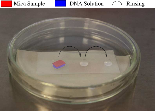
In order to achieve a reproducible deposition of -DNA onto mica the following protocol was suggested to us by D. Klinov. In order to obtain stable humidity conditions during DNA deposition, the sample and DNA solution are kept in a closed petri box with wet filter paper at the bottom (see Fig. 2). A drop of DNA solution (volume ) is deposited onto the clean side of a para-film sheet folded around a glass slide. The freshly cleaved mica sample is then deposited on top of the drop (clean side facing down). This reduces the area of the water-air interface during deposition and reduces the contamination of the drop. After 10 minutes, many -DNA molecules are attached to the mica surface at several anchoring points and the sample can be moved onto of a purified watter droplet where salt residues are left to dissolve for around 10 minutes. This rinsing process is repeated two times.
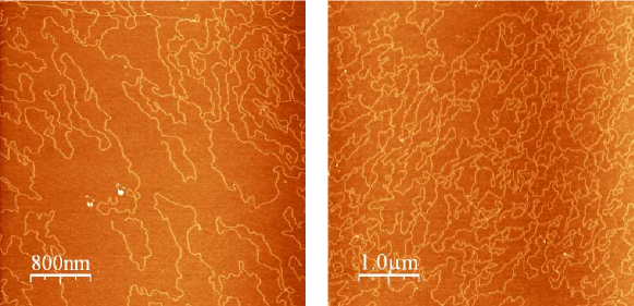
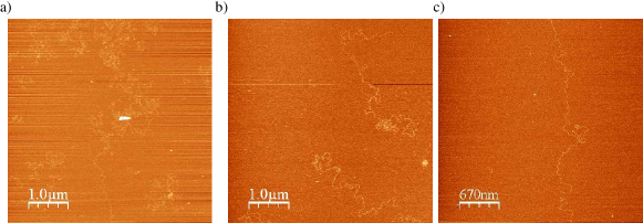
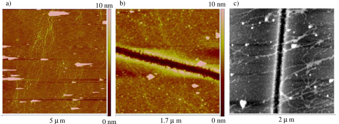
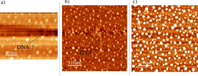
The above protocol allows to achieve reproducible DNA deposition due to several advantages. DNA molecules have the time to adsorb on the surface before they undergo the force of the meniscus during the drying of the sample, hence they are attached in a state where they are not overstretched and keep their natural persistence length. Two AFM images from different samples are shown on Fig. 3, in both cases AFM shows long molecules undulating on a clean substrate with very little contamination. This deposition experiment allows us to check that our DNA solution has the right concentration and is not contaminated by undesired chemical substances.
The measured height of DNA is around nm, which contrasts with measurements of DNA height on mica in liquid AFM cells where height around nm can be observed Hansma . Several explanations can be put forward to explain this discrepancy. It is possible that a water hydration layer forms near the DNA molecules reducing the apparent height of the molecules. Another hypothesis is that DNA may be strongly denaturated by the strong interaction with the surface when the sample is dry, which can create a transition from B-DNA to A-DNA. However we note that there is no significant difference in DNA diameter for A and B forms of DNA PNASab .
For overstretched molecules a transition to the Pauling’s P-DNA form is possible and the molecule thickness may indeed be close to a nanometer since the phosphate backbones are tightly interwound and the bases are exposed to the exterior of the molecule Croquette . After deposition of DNA we check that the molecules absorbed on the substrate have a persistence length close to their natural persistence length in solution. This ensures that we apply a very limited strain on the molecules and transition to P-DNA form seems unlikely in most of our experiments (see Fig. 3 for undulating molecules, examples of overstretched molecules are shown on Fig. 4).
II DNA deposition onto metallic surfaces
For transport measurements DNA must be deposited on a metallic substrate. Many metals (for example Aluminum, Copper, …) can form a thin insulating oxide layer on their surface in atmospheric conditions. While the oxide layer does not influence conduction properties in the bulk of the metallic film, it can prevent the formation of an electrical contact between DNA and the metallic electrodes. Hence the choice of material for electrode is limited to noble metals. For experiments on DNA mainly gold, platinum and rhenium have been used so far Endres although carbon based materials (carbon nanotubes, graphite) emerge as a promising material for contacting DNA electrically Barton .
In our experiments we have used a thin Platinum metallic film of a few nanometers (typically between 3 and 5 nm) deposited by Argon DC-plasma sputtering on a freshly cleaved mica surface. Since platinum is deposited everywhere on the sample, no further chemical processing is needed and the obtained metallic surface is very clean and chemically inert. As a result there is in principle no binding sites to attach DNA molecules to the substrate, and we do not expect DNA adsorption. This is not completely true however since DNA molecules have active chemical end groups. For example it has been proposed that in certain pH ranges DNA ends can expose hydrophobic domains of the bases and bind to hydrophic surfaces pHens . Hence it is possible that DNA molecules bind to platinum through their extremities.
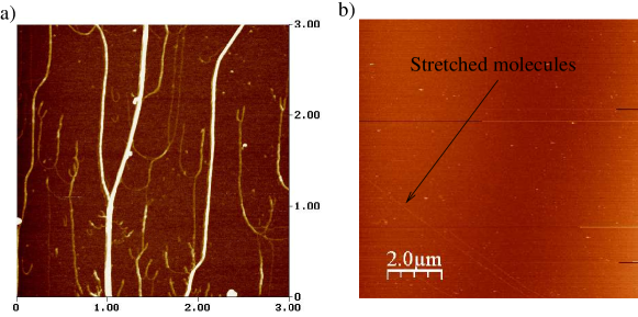
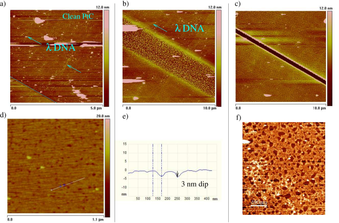
If the DNA solution is incubated a few minutes on the sample both ends of the molecule have in general enough time to attach to the substrate. Once the sample is dried the molecules are stretched by the water flow leading to a characteristic “U” shape of the molecules when the substrate is analyzed with an AFM (see Fig. 4.a). As molecules already present on the substrate create additional binding sites for the adhesion of other molecules in the solution, many ropes of DNA molecules can be observed on the Platinum substrate. Note that the formation of ropes is less likely if the sample is incubated for a shorter time (or rinsed under a continuous flow), in this case (see Fig. 4.b) AFM images show only a small number of stretched DNA molecules which are mainly attached through one of their extremities.
In the above procedure the DNA molecules were deposited onto the platinum film directly after sputtering. Of course transport measurements can not be realized in this configuration. Transport measurements are possible only after electrodes have been patterned on the substrate. The simplest way to fabricate an insulating gap is to protect the regions where we do not want deposition by a MMA/PMMA resist that can be patterned beforehand using usual electron-beam lithography techniques. After sputtering the resist is dissolved in hot acetone and a gap is formed. The presence of organic residues originating from imperfect removal of the PMMA film changes the adsorption properties of DNA molecules on the substrate. On this “contaminated” substrate it becomes possible to deposit molecules without over-stretching or creation of ropes (see Fig. 5) although the success rate is small since the surface state of these samples is rather poorly controlled (indeed in many cases DNA molecules do not bind at all to sample). These sample showed insulating behavior even if several DNA molecules crossed the gap between the electrodes (see for e.g. Fig. 5, shortest distance between electrodes was around in this sample). This insulating behavior is consistent with the experimental findings from Storm , which indicated that DNA is an insulator when it is deposited on Silicon/and mica surfaces.
Because of the poor reproducibility of DNA deposition on bare metallic samples, and confirmed absence of conduction we subsequently focused onto deposition of DNA on metallic electrodes functionalized by a pentylamine plasma as proposed in Refs. Kasumov ; Klinov where conduction on samples with DNA was observed at low temperature.
III Pentylamine plasma functionalization for deposition of DNA molecules

The use of the pentylamine molecule (see Fig. 6) was introduced by Dubochet Dubochet as a mean to render carbon support films for electron microscopy hydrophilic in order to make possible adsorption of biological molecules. The sample is commonly placed between two parallel electrode plates in a vacuum chamber with weak pentylamine pressure (). A high voltage () is then applied to the plates creating a glow discharge. The ionic species produced during the discharge are deposited on the substrate and create a positively charged background favorable for DNA adsorption (typical discharge time was in our experiments, reported pressure and voltage values correspond to those used for the setup in the group “Microscopie moléculaire” at Institut Gustave Roussy).
The chemical structure of the deposited chemical species is not well characterized and is certainly complex (see also Table 2). For example it is known that a discharge of an gas mixture, creates ions and radicals Liberman Note however that the fraction of dissociated species among the gas molecules is usually very small (of the order of ) in this discharges used for material processing, hence it is highly probable that not only dissociated molecules are deposited on the substrate.
| Bond dissociation energy | kJ/mol |
|---|---|
| 450 | |
| 439 | |
| 376 | |
| 336 | |
| 297 | |
| Ionization energy | kJ/mol |
| 1312 | |
| 826 | |
| 726 |
The pentylamine discharge technique was adapted to attach DNA molecules to conducting electrodes in the experiments from Refs. Kasumov ; Klinov . It constitutes the main difference with other studies where in most cases the substrate was silicon dioxide. Hence we dedicated considerable efforts to identify the substrate on which this treatment yields effective binding of DNA molecules. These studies led us to the conclusion that reproducible adsorption of DNA with pentylamine treatment occurs only on carbon coated substrates, which are similar to the carbon support films for electron microscopy. In this respect the analysis in Klinov is somewhat misleading since it claims that pentylamine can form a polymer film on mica suitable for adsorption of DNA. Below we summarize the results of our DNA deposition experiments on different substrates using the pentylamine technique. In all cases the DNA deposition was attempted rapidly (at most one hour) after the glow discharge since we have observed that the efficiency of the pentylamine layer at binding DNA molecules decreases quickly once it is exposed to ambient air.
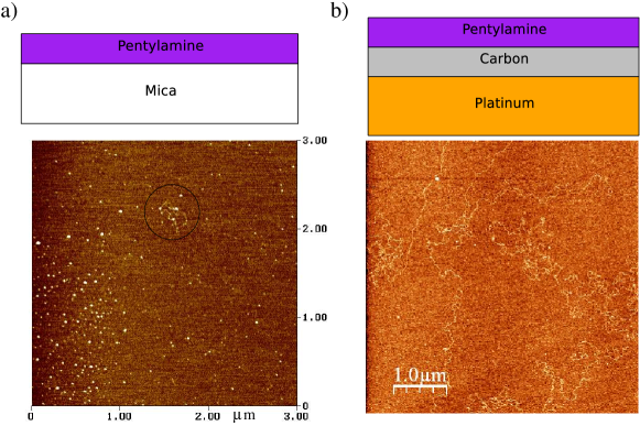
Our attempts to deposit DNA on a freshly cleaved mica substrate functionalized by pentylamine plasma were never successful. An example AFM image of the mica substrate after pentylamine plasma and DNA deposition is shown on Fig. 7. Only a single feature reassembling a DNA molecule can be distinguished inside the scan area : this is much less than the number of molecules on the Figs. 3,5 which have similar scan size. The absence of molecules on the mica substrate is puzzling since DNA binds to both pentylamine functionalized surfaces and bare mica. A possible explanation is that in a first stage molecules bind to the pentylamine film on top of the mica surface. In a second stage this film is washed away from the surface when the sample is dried ripping away the DNA molecules on top of the pentylamine film. Indeed the pentylamine film must be destroyed at some stage of the deposition because the density of DNA molecules on the surface is extremely small compared to the densities achieved on the Pt/C surface with the same functionalization. It can not be destroyed immediately when the drop is deposited on the surface, otherwise DNA molecules would bind to the exposed mica surface. To summarize in the above scenario pentylamine masks the mica surface from the DNA solution and is at least partially removed when the sample is dried, carrying away the attached DNA molecules (this assumes that the layer formed during the plasma discharge is continuous).
Deposition of DNA molecules on a platinum film coated with an evaporated layer of amorphous carbon (around 10 nm) were reproducible and successful (see Fig. 7). Most likely the free radicals created during the glow discharge react with the amorphous carbon on the surface, and anchor the pentylamine layer. As seen in this image the molecules are not overstretched, it may also seem that their persistence length is smaller than on the mica substrate (see Fig. 3). This observation is supported by other quantitative studies of DNA adsorption on positively charged surfaces DnaPositive . Following Ref. Klinov we have also tried to deposit DNA with the pentylamine treatment directly onto platinum without the carbon layer. For clean platinum films only a low density of overstretched molecules could be detected on the surface after DNA deposition. This most likely indicates that the pentylamine is removed during the DNA deposition and only a few molecules bind to the platinum surface through their ends with a mechanism similar to that described in Section II. After discussions with D. Klinov, we found that the Platinum deposited in Klinov actually contained a certain amount of carbon (around 10%) which allowed fixation of the pentylamine.
In conclusion the adhesion of the pentylamine is reliable only on surfaces with a high enough density of carbon atoms that can bind with the ions/radicals produced during the glow discharge sticking the pentylamine to the surface. In this case the deposition of DNA molecules is reproducible and molecules are not overstretched. The role of the carbon atoms is only to anchor the pentylamine layer. Hence it is not necessary to form a continuous carbon coating of the substrate. For example the Pt/C samples produced by D. Klinov were obtained by simultaneous evaporation of both Platinum and Carbon in unknown proportions. (However in the transport devices for measurement of DNA transport the nature of the substrate will not be relevant since the active region will be contaminated by carbon from the focused ion beam microscope).
IV Combing DNA molecules onto electrodes with the pentylamine technique
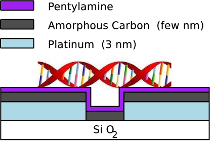
In the previous section we described how DNA molecules can be attached on a metallic film with the pentylamine plasma functionalization. From our experiments it seems that this procedure is successful at attaching DNA molecules only on carbon coated substrates. In this section the substrate will be a Platinum film (3 nm) sputtered on a cleaved mica surface and covered by a layer ( of evaporated amorphous carbon).
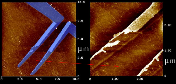
We now describe how to orient DNA molecules perpendicularly to an insulating gap separating wide metallic electrodes. The possibility to orient individual DNA molecules with a moving air-liquid interface was first established experimentally in Ref. DnaCombing . Figure 8 shows a photography of the deposition setup, and an AFM image of the molecules at the metal-insulator interface (both were covered by an amorphous carbon layer before deposition). Even if molecules are combed on the electrodes, they seem to turn around at the metal boundary avoiding the insulator. This guiding may be explained by pinning of the liquid air-interface at the border between the two regions. Moreover many molecules are overstretched which is to be avoided for transport measurements. For this reason we have chosen an alternative technique which consists in orienting the molecules with a flow. A macroscopic Poiseuille flow is not perturbed by defects and interfaces on the nanoscale, and regulation of the flow velocity allows in principle to control the elongation of the molecules.
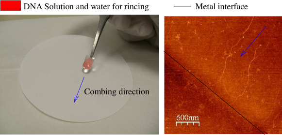
In our deposition protocol (see Fig. 9 for a description of the setup) the droplet is first incubated on the sample surface for around a minute. This allows DNA molecules to bind to the surface at a few contact points without complete adsorption on the surface. Afterward the rinsing flow is turned on, it provides a flow rate of of pure water on the sample. This flow has a double function of combing DNA molecules and rinsing salt residues that may form on the surface rendering AFM imaging difficult. It is interesting to know in which flow speed regime DNA molecules may start to be overstretched. A quantitative study of the dynamics of a tethered DNA molecules under a Poiseuille flow was performed recently DNAflowENS using fluorescence microscopy.
It was found that the elongation of the molecules was governed by a single dimensionless parameter, called the Weissenberg number where is the shear rate and is the longest relaxation time of the DNA molecule (it was found to be for -DNA labeled with fluorescent beads DNAflowENS ). Complete elongation of the molecules occurred only for , while an elongation of occurs already for . The shear rate in our experiments can be estimated as follows: the outflow of liquid on the surface is , for a cross section of the droplet of the order of where is the droplet height and is the droplet radius. The mean velocity in the fluid is and since the flow vanishes at the contact with the substrate the shear rate is leading to . This calculation shows that with our typical flow parameters we are far from the threshold where molecules may start to be overstretched. As a result we have set the debit to a value around where the flow on the sample was stable without risks of uncontrolled drying of the drop during the rinsing process.
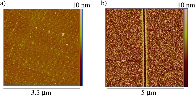
AFM images of DNA molecules deposited with this technique on a carbon coated platinum surface are shown on Fig. 10. The extension of molecule depends on the number of active binding sites created during the glow discharge, the incubation time before rinsing and on the water flow rate. Since all these parameters are hard to fix in a reproducible way, sometimes molecules are more collapsed onto themselves (Fig. 10.a) and sometimes they are more extended (Fig. 10.c). However binding and orientation of the molecule (in the range suggested by the different cases of Fig. 10) was reproducible with this technique.
Now all ingredients are assembled to deposit DNA molecules across an insulating gap using the pentylamine technique. We have done this with electrodes produced with both electron beam lithography and focused ion beam etching (this technique was also used in Klinov and will be described further on in Section V). A cross section of the material layers constituting electrodes and the gap is sketched on Fig. 11, this structure is similar for both electron-and ion beam processed samples. The width of the gaps for these samples was between and . Molecules crossing the gap are clearly visible in Fig. 12 however all the gaps where we deposited molecules always remained insulating with resistances larger than Giga-Ohms despite presence of carbon and pentylamine layers. In order to verify that the surface of the electrodes is not insulating due to the formation of an oxide layer or due to organic contamination we have deposited HIPCO single wall carbon nanotubes (SWNT) from a dichloroethane solution across the electrodes. The resistance of the junction then dropped to values of the order of suggesting that our electrodes were clean enough to make contacts to nanonotubes. However we will argue in the next sections that the electrodes were probably covered by an insulating pentylamine layer during deposition of DNA molecules. The organic solvent of the SWNT may have cleaned the electrode surface thereby allowing the formation of an electrical contact.
These results are in disagreement with findings from Kasumov ; Klinov which suggested that the presence of a pentylamine layer creates a suitable substrate where conduction of DNA molecules is possible. However the above experiments depend on many parameters which are often poorly defined. In the absence of any credible indication on the origin of this discrepancy we have asked D. Klinov to deposit DNA molecules with his setup on samples with insulating gaps prepared in our laboratory using a focused ion beam reproducing as accurately as possible the experiment from Ref. Klinov .
V Fabrication of narrow insulating gaps using a focused ion beam
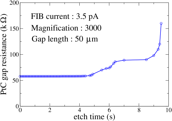
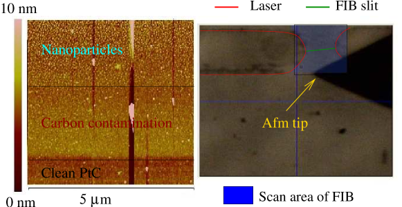
This method of fabrication of insulating gaps does not use electron beam lithography and therefore avoids the contamination of the surface by residues from organic resist. A thin layer of platinum carbon was deposited in D. Klinov’s laboratory on a freshly cleaved mica substrate. This metal layer has an estimated thickness of at around and a resistance per square of around . A schematic representation of the sample layout after laser and focused ion beam (FIB) etching is shown on Fig. 13. In a first step thick gold () contact pads were evaporated through a mechanical mask. We then cut long trenches in the metallic film using an ultraviolet focused laser with spot-size around to . The laser locally heats the surface and evaporates the metal layer creating holes in the metal of the order of the spot size. Programmable motors then allow to expose the metal in predefined patterns around the golden contacts leaving regularly spaced metal openings long. These remaining metal stripes were opened with a Gallium FIB which can etch narrow wide trenches. In order to determine the minimal dose of FIB irradiation required to produce a narrow insulating gap in the platinum film we have developed a technique for in-situ measurement of the film resistance inside the FIB microscope.

This technique allows us to continuously monitor the resistance between several gaps contacted in series (for e.g. between the hatched regions on Fig. 13). First an estimate of the required etch time is obtained by cutting half of one gap and monitoring simultaneously the increase of resistance as a function of time. We estimate the optimum etching time of the PtC film from the value at which the resistance saturates. After this operation the measured resistance is still finite since only half of the gap is etched, this allows to repeat the operation and accumulate statistics on a few (typically 5) gaps. At the last step one of the gap is opened completely until resistance diverges, the resistance dependence on the etch time is shown on Fig. 14 for one of the junctions. This last measure gives a very precise estimate of the minimal dose. Considering possible fluctuations in the thickness of the film, we increase this dose by around 20% and etch all the remaining gaps with the same dose.
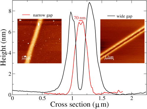
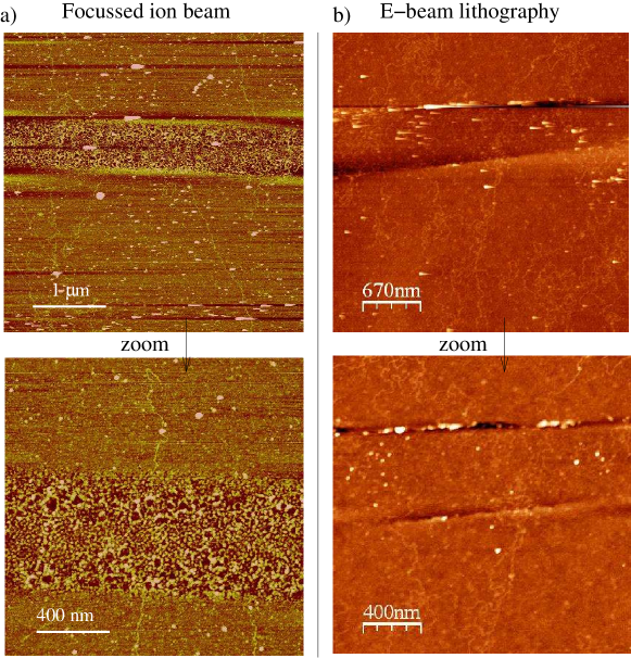
Atomic force microscopy images of the gaps fabricated with the FIB are shown on Fig. 15. For the narrowest gap the height profile exhibits a characteristic peak with a small dip in the center where the gap is insulating. Certainly the dip is actually deeper than shown on the AFM image because of tip convolution effects. At higher irradiation doses, the gap grows in size and more pronounced side peaks appear.
Surprisingly for the minimal etch time, the width of the insulating region is of the order of and is very slender compared to the contamination peak which extends over about . The cross section of the peak for the narrow gap is where is the gap height, and are respectively the bump and gap widths. Assuming that the thickness of the platinum film is around we find that the cross section of the excavated platinum is sensibly smaller . It is possible that FIB dug also into mica providing the remaining material inside the bump. However since we stopped etching just when the gap became insulating, it is unlikely that we dug very deep into the mica surface. It is instructive to compare the number of atoms inside this “bump” (we find that where is the gap length and is the average distance between atoms for e.g. in a gallium crystal), with the number of gallium atoms sent by the FIB. This number can be estimated from the FIB current and the etch time for the narrow gap on Fig. 14, it amounts to (e is the elementary charge). According to this calculation there is an almost two order of magnitude difference between the quantity of atoms in the bump and the quantity of atoms emitted by the ion beam . Although these estimates are not very accurate they suggest that there may be a third origin for the peaks around the gap other than displacement of platinum and mica and injection of gallium atoms. It is possible that the metallic film dewets locally from the mica surface due to heating by FIB creating a bump (we have remarked adhesion of thin films is generally not very good on mica). In all cases AFM scans in the direction parallel to the gap show ( see AFM images from Fig. 12.a ) that the surface is very rough in a region extending across much wider than the insulating region (), indicating that the PtC film is damaged or contaminated in a large region outside the gap.
For the moment we stop here the analysis of the gap structure (but it continues in Section VII !). In the discussion that follows, it is enough to keep in mind that the structure of the gap may actually be quite complicated even if it is obtained by “physical” means without organic resists.
A total of about twelve substrates were sent to D. Klinov in Moscow for the deposition of DNA molecules, with about ten gaps opened by FIB on each sample. The deposition protocol used by D. Klinov seems similar to the protocol we used in our deposition experiments (see Section IV). The only difference is that in D. Klinov’s pentylamine setup a gas flow continuously refreshes the pentylamine gas in the discharge chamber. This procedure can reduce the probability of forming radicals/ions which require breaking several bonds or removing several electrons from the pentylamine molecule. But this probability is low anyway and it is not clear how it could influence the conduction of DNA.
The results on conduction after deposition of DNA molecules in D. Klinov’s laboratory are summarized in Table 3. On three samples conduction was observed after deposition of DNA molecules across slits that were insulating before DNA deposition. The statistics on these three sample is very favorable since 11 out of 15 slits became conducting. Moreover the deposition protocol was repeated with a buffer solution without DNA on a control sample from the same batch as two of the conducting samples (the mica sample was cut in three pieces before the pentylamine treatment) and all the 14 gaps remained insulating. This statistic is strongly in favor of an interpretation in term of conduction through DNA molecules. However this statistical argument must be handled with care. If we consider all the samples were deposition of molecules was attempted, the conducting slits represent only around 10% of the prepared structures. On the other samples or no DNA molecules could be detected with AFM indicating that pentylamine functionalization was not effective or the molecules were insulating. Hence observation of conductivity after attempts of DNA deposition has actually a low success rate even when deposition is done by D. Klinov following the recipes used in Kasumov ; Klinov . We have reached the conclusion that one of the reasons behind this irreducibility lies in the structure of the sample after etching which will be discussed in more detail in Section VII. We now turn to transport measurements on the three samples where conduction was observed.
| Number of substrates | 12 |
|---|---|
| Number of FIB slits | 100 |
| Number of substrates with visible DNA | 5 |
| Number of substrates with conducting slits after deposition | 3 |
| Number of conducting slits after deposition | 11 |
| Number of slits on these three subtrates | 15 |
| Number of slits on the control sample | 14 |
| Number of conducting slits after buffer | 0 |
VI Transport measurements on conducting DNA samples
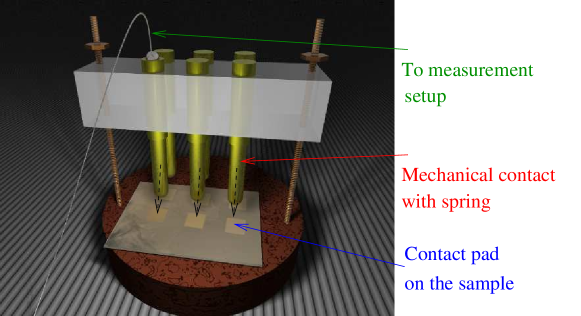
Before performing transport measurements on the three substrates where conduction appeared after deposition of DNA molecules we had to connect the samples to a sample holder which can be mounted inside one of our dilution fridges. This connection can be realized through thin ( diameter) wires with ultrasound bonding or glued with silver paint. Ultrasound bonding on a sample with three conducting gaps, led to disappearance of conduction on three gaps. It is possible that an electrical discharge was created during the ultrasound bonding destroying the conduction across our samples. In order to avoid this discharge we have decided to contact the second sample using silver paint. Surprisingly with silver paint conduction was also destroyed on the five conducting gaps of the second sample. During the process of contacting the gaps we checked their conductivity under a test-probe several times. The resistance of a gap could change even when the silver paint drops were deposited on the contact pads of the other samples. For example the resistance across one of the gaps took the following values: . These observations suggested that our samples were sensible to the vapors of the silver paint solvent. Hence we decided to avoid silver paint for the contacts on the last sample. A possibility was to replace silver paint with indium paste however the latter did not stick to contact pads after the pentylamine discharge probably because of the presence of the organic layer. A. Kasumov then proposed to use a system of mechanical contacts with springs that we fabricated specially to fit the geometric parameters of the last remaining sample (see Fig. 16).
This allowed us to contact 5 conducting gaps which we measured at low temperature. Their resistance at room temperature is listed in Tab. 4
| measured at low temperature | |||||
| measured only at room temperature |
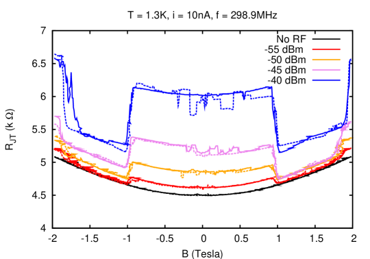
To our surprise all four samples with room temperature resistance exhibited superconducting behavior at low temperature. Indeed contrarily to the experiment Kasumov where superconducting electrodes where used to contact the DNA molecules, our platinum/carbon contacts are in a normal state. The dependence on temperature for different magnetic fields is shown for two samples on Figs. (17,18). Superconductivity appeared below and results in a drop of resistance that saturates at low temperature because of the finite resistance of the normal contacts. The 10 sample displayed a very smooth transition as a function of temperature (see Fig. 17) and the drop of resistance saturated at . In contrast less resistive samples had a sharper transition (see for e.g. Fig. 18) with a saturation temperature around . The smooth transition observed in the 10 sample has some similarities to smooth transitions observed in Superconductor-Normal-Superconductor (SNS) junctions in the intermediate regime between a long and a short junction. A long SNS junctions is characterized by the presence of two transitions. The transition at the highest temperature, stems from the transition of the superconducting contacts while at a lower temperature proximity induced superconductivity sets-in in the normal region Lionel . When the length of the normal part is decreased the two transitions merge into a single smoother transition KasumovSWNT ; KasumovSWNT2 . Since in our samples only a single transition is observed, this suggests that we have created an SNS junction in this intermediate regime.
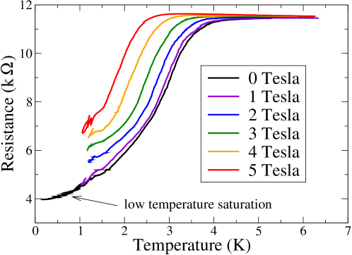
A possible origin of the superconductivity is the Gallium contamination deposited by the FIB. An insight on the size of the superconducting contamination islands is provided by the dependence on magnetic field. Under a magnetic field the resistance of the samples increased, however the maximal magnetic field available in our setup () was not sufficient to completely destroy superconductivity at low temperature indicating a critical magnetic field of the order of (see Figs. 17 and 18). Assuming the presence of superconducting nanoparticles we can also understand the origin of this relatively high critical field. The magnetic field destroys superconductivity in a nanoparticle when it creates a flux of the order of the flux quantum through the nanoparticle surface where is the nanoparticle radius. This criterion gives a typical nanoparticle radius of the order of . Through extensive AFM/SEM characterization of the measured sample (see Section VII) we were able to establish that these nanoparticles were deposited by FIB. Gallium is superconducting with transition temperature , the presence of carbon impurities may increase this transition temperature to . Indeed tungsten wires deposited with FIB containing Gallium and carbon have critical temperature whereas the pure tungsten has critical temperature around Kasumov2 . Thus it is probable that the source of superconductivity are superconducting nanoparticles inside (and even outside !) the gap cut by the FIB. The nanoparticles themselves can not give rise to ohmic resistances of a few , hence the large amplitude of the resistance (drop for e.g. from to ) between the normal and the superconducting states, indicates a configuration where a normal nanowire connecting the contacts is rendered superconducting by proximity effect from the nanoparticles. To conclude on the dependence on magnetic field, one of the samples displayed SQUID like modulation in the magnetoresistance with a period of at temperature . These oscillations disappeared at lower and higher temperatures and suggesting a complex geometry with several SNS junctions connected in series and/or in parallel.

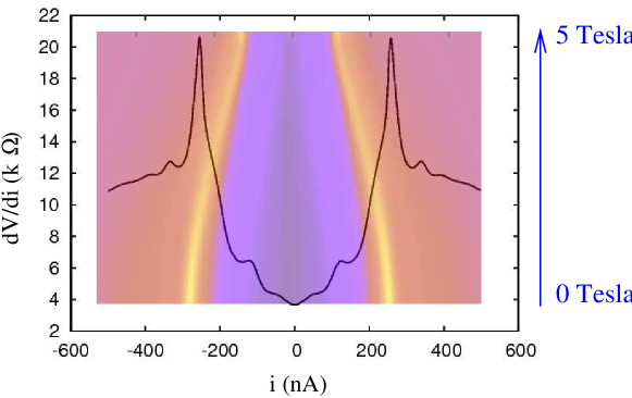
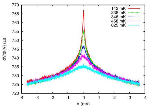
We have also measured the differential resistance of the sample as a function of a DC current. The results for the sample are shown on Fig. 19 and resemble the data obtained from Ref. Kasumov on DNA samples with superconducting Rhenium contacts. At zero magnetic field the differential resistance exhibits a large drop in the current interval . Inside the gap region the resistance drops smoothly but does not vanish probably because of the contact resistance of the normal electrodes. In our interpretation the large peak at corresponds to the critical current of a nanoparticle. The smaller peaks may appear due to other nanoparticles weakly connected in series or in parallel in our conducting junction. As suggested by the colorscale diagram, the critical current decreases when a magnetic field is applied. At the maximal available magnetic field , the critical current is since as stressed above our magnetic fields are not strong enough to completely suppress superconductivity. The three other less resistive junctions give similar dependence (see Fig. 20). In these other samples more peaks are apparent and one of the junctions was hysteric. Figure 20 also presents the low temperature differential conductance of the resistive junction with room temperature resistance of 10. At low temperature this sample becomes insulating at low bias voltage. When the bias exceeds the conductance starts to increase following a cone shape typical for graphite but a priori unexpected in our samples. An hysteric singularity appears when the bias reaches a value around . Although it is hard to determine with certitude the origin of this hysteresis we note that is close to the estimated HOMO-LUMO gap in DNA and that similar singularities were observed at room temperature in the conduction of DNA/lipid films confined between nanogaps Kasumov3 . In this respect this is the only sample whose DC transport characteristics can hardly be mimicked by a metallic short-circuit of very small dimensions.

In order to search for sample characteristics which might be specific of DNA molecules we have irradiated our samples with microwaves. Our idea was that the helix structure of the molecule could induce special magnetic field asymmetry in the out of equilibrium transport across the molecule. This expectation was not confirmed experimentally since the dependence under irradiation remained rather symmetrical. However the DC-magnetoresistance of our samples could become unstable under microwave irradiation (see Fig. 21). Interestingly instabilities were observed mainly at rather low frequencies . A possible (although science fiction like) interpretation is that the microwave field excites a mechanical transition between two possible equilibrium positions for a DNA molecule suspended across the peaks created on both sides of the gap by the FIB etching; in this scenario the superconductivity just enhances the sensibility to these mechanical vibrations. However one must take into account that the response to microwave may be very complicated in superconducting weak links where the switching may become chaotic. In particular magnetic field anti-symmetric photovoltaic effect was observed in such systems by Bartolo . Hence the presence of a magnetic field asymmetry does not allow to discriminate between a chiral molecule like DNA and an array of superconducting weak links.
In the above experiments we have assumed that superconductivity was induced by superconducting nanoparticles because of the high critical magnetic fields. Yet it is not the only possibility since FIB irradiation can induce superconductivity in materials with otherwise very small critical temperatures. For example the tungsten deposited under FIB has critical temperatures around and a high critical magnetic field of . Hence there is also a possibility that the Pt bumps observed on the edges of the gap (see Fig. 15) could become superconducting due to a high concentration of incorporated Gallium atoms. In order to check experimentally if this is indeed the case we have deliberately prepared a short-circuit across a clean Pt film by stopping the FIB etching before the gap became completely insulating (this may be compared with Fig. 14 where the metallic film was etched until the gap became insulating). In this control sample superconductivity was absent, but low temperature measurements revealed a low bias differential resistance peak increasing at low temperature (see Fig. 22) in a behavior reminiscent of dynamical Coulomb blockade Klinov . The effect in Fig. 22 is smaller by an order of magnitude compared to Ref. Joyez . This is probably because we measured a short-circuit much more conductive than conductance quantum, however short-circuits formed by FIB can be more resistive see for e.g. Fig. 14. Hence it is plausible that FIB etching can create quasi-one dimensional filaments inside the gap capable of producing dynamical coulomb blockade behavior.
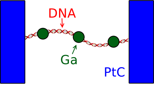
In general these superconducting nanoparticles are unlikely to induce superconductivity in a normal metallic conductor because of the inverse proximity effect. Direct proximity effect is possible in this regime only if the density of states in the normal metal is very low. For example it was recently proposed that nanoparticles could induce superconductivity in graphene Kostia . Since DNA molecules have a very low density of states they are good candidates for forming the normal region of our SNS junctions. The image that then comes to mind (see Fig. 22) is that of a DNA molecule connecting several nanoparticles and connected to the normal PtC contacts.
However it is also possible that the nano-filaments created by FIB can be small enough for the direct proximity effect to be possible. Indeed, even if the gaps were insulating before deposition of DNA, one can imagine that the metallic residues inside the gap could have been displaced by the DNA molecules creating a leak. Note that the absence of superconductivity in the control sample from Fig. 22 does not rule out this scenario. Indeed we will show in the next section that the deposition of nanoparticle is not a reproducible phenomena and a single control short-circuit sample may not be representative. It is actually hard to discriminate between these two possibilities. Our samples do not have a backgate since they are prepared on mica, heating up to the denaturation temperature of DNA is not possible since pure Gallium melts at low temperature of and experiments in liquid may simply break the device by removing the pentylamine layer. As a result we have chosen ultraviolet (UV) irradiation as the most distinctive experiment, indeed it is well established that UV can damage the DNA molecules whereas it is not harmful for a metallic film provided that there is no heating from the UV lamp. We tried to irradiate one of the samples with an UV irradiation with wavelength . The electrical conduction disappeared immediately (on the scale of seconds) after the UV lamp was switched, whereas the resistivity of a platinum film of a few nanometers thickness did not change after an hour of irradiation. Even if this experiment is spectacular it is not necessarily conclusive because an electrical discharge could have occurred when the lamp was switched on (the lamp and resistance measuring equipment are connected through a common connection to the ground). Probably in future experiments UV must be attenuated to observe a more progressive transition.
If our interpretation in term of proximity-induced superconductivity in DNA molecules is valid, the number of peaks in the differential resistance measurements (see Fig. 19 and Figs. 20.a,b,c) gives an estimation of the number of nanoparticles connected to the DNA molecules that transit to the superconducting state. Two limiting cases may occur depending on the number of connected DNA molecules that exhibit proximity induced superconductivity :
-
•
1. It is possible that only a single molecule transits into the superconducting state. In this case each peak in the differential resistance should correspond to the critical current of a DNA molecule connected to superconducting nanoparticles and the number of peaks should give the number of nanoparticles connected to the superconducting DNA molecule. In our samples the number of peaks varies from to (sample from Fig. 20.b and Fig. 20.a respectively). By dividing the average length of the gap by the number of connected nanoparticles, we can estimate the typical length of the individual DNA segments that connect neighboring nanoparticles (see Fig. 23 for a sketch of the geometry). For a gap width of approximately , we find that this length scale varies from to .
-
•
2. In the opposite limit, we can assume that there are only two connected nanoparticles per superconducting molecule. Under this assumption the number of peaks gives the number of superconducting molecules. The transport in DNA molecules in this configuration is typically probed on a length scale corresponding to half of the gap width: .
In conclusion the conductivity of DNA molecules is probed on a length scale between and which is smaller than the width of the insulating gap which is around wide. We note that transport in DNA on a scale was reported by several independent groups for e.g. Porath ; Barton .
VII Characterization of the gaps from our transport experiments
The topography characterization of the gaps etched by FIB was already exposed in Section V and we will start this characterization section by describing the scanning electron microscope (SEM) images of our gaps. SEM provides a strong contrast between insulators and metals, whereas AFM in tapping mode is only sensible to topography. Hence SEM is a good technique to detect metallic residues inside the gap where the topography is rough after FIB etching. Note that no careful SEM analysis of the gaps was done in the previous experiments Kasumov ; Klinov , however it is very likely that the gaps used in these experiments had a similar structure specially in Klinov where they were also fabricated by FIB.
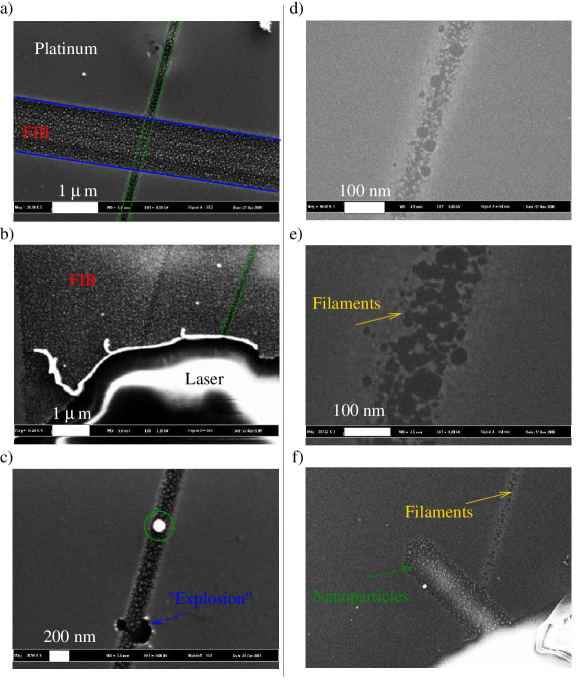
Several SEM images of the FIB gaps are displayed on Fig. 24, intriguingly in all the images metallic contamination is present in the gap after etching. Two possible limit situations seem to emerge from our observations. In the case where the FIB dose is weak the metallic residues take the form of filaments (Fig. 24 right panel) whereas after a stronger dose the residues seem to form an ordered network of nanoparticles (Fig. 24 left panel). This transition may be inferred from Fig. 24.f, where two neighbor regions were etched with different FIB doses under the same beam conditions. In the narrow trench filaments can be clearly distinguished (see also Figs. 24.d,e ) while in the wider trench where the dose was stronger residues form individual nanoparticles. Naturally one can expect the residues to disappear after a sufficient FIB dose. This dose however seems difficult to attain in practice. This difficulty is illustrated on Figs. 24.a,b. In the first figure two intersecting regions were etched with FIB (they are highlighted by blue and green lines). Both regions were exposed to a dose sufficient to etch most of the metallic film leaving isolated nanoparticles inside the gap. Surprisingly the density of nanoparticles does not decrease in the intersection between these two regions (parallelogram with edges formed by blue and green lines) even if the intersection area received a dose about two times larger than the other regions. A similar situation is observed on Fig. 24.b, where a large area was etched by FIB irradiation around a slit cut by FIB (delimited by the parallel green lines). The region inside the slit still contains nanoparticles even if it received twice an irradiation dose capable of etching most of the platinum film. As a result the dose needed to completely etch all metallic residues, is certainly much larger than the minimal dose required to create an insulating slit.
The presence of nanoparticles has two possible origins, an instability of the gallium tip that can start to emit small nanoparticles instead of individual gallium ions and the recombination of the gallium atoms on the mica surface (the latter mechanism is then specific to mica since it is not observed on ). Our observations suggests that both mechanisms are possible. On one sample we have detected nanoparticles everywhere inside a large square area corresponding to the scan size of the FIB (see Fig. 25). This proves that in some uncontrolled regime FIB is capable of disseminating small nanoparticle instead of individual gallium ions. The above behavior was observed on only a single sample, however this was the sample that we studied at low temperature in Section VI, hence this rather special case is very important for the interpretation of our transport measurements. In other samples nanoparticles were observed only inside the gap indicating a different origin. It may be possible that Gallium atoms recombine on the mica surface to form nanoparticles. Note that a similar behavior has been observed on GaAs substrates OrsayPhysics and the presence of Aluminum atoms in mica substrate may play a role.
The atomic force microscopy measurements on the edge of the FIB scan window depicted on Fig. 25, revealed another source of contamination. A step of height systematically surrounded the FIB scan window, this contamination layer is probably composed of carbon deposited during FIB imaging of the gaps (similarly to a contamination layer deposited under SEM). This is actually very discouraging because the FIB technology was chosen because it supposedly limited contamination. In reality the electrodes are covered by a poorly characterized carbon contamination layer. As a side consequence this makes the debate on platinum versus platinum carbon electrodes not pertinent near the slits.
We will now summarize the different contamination sources that were revealed through SEM and tapping mode AFM microscopy. On mica substrate it seems that metal residues are always present inside the gap (at least for practically reasonable FIB doses). They can take the form of narrow filaments for low FIB doses or a net of nanoparticles at high doses. An exceptional regime can also occur where the gallium tip of the FIB becomes unstable and starts to stew nanoparticles everywhere in its scan area. From our experiments this case seems rather improbable however it occurred at least once, on the sample that we measured at low temperatures. Finally a carbon contamination layer is deposited near the gap during the imaging inside the FIB microscope. Keeping in mind the above information, we will now focus on the detection of DNA molecules across the gaps where conduction was observed after deposition of DNA molecules.
In previous experiments Kasumov ; Klinov DNA molecules crossing FIB slits could be detected with tapping mode AFM. However AFM and low temperature transport measurements were done independently, and probably on different samples while we know that fluctuations are very strong from one sample to another. Thus the correlation between the presence of DNA molecule and the appearance of electronic transport was supported only by a statistical argument (absence of conduction on control samples when a buffer solution without DNA was deposited). Here we tried to detect DNA molecules on the three samples where conduction was induced after the deposition of DNA molecules with the pentylamine technique was attempted.
We will start with two samples where conduction was destroyed during the attempts to contact the samples electrically (see SectionVI). In one of the samples DNA molecules could be observed both in the region far from the gaps where PtC was clean and inside the area covered by the carbon contamination film near the gap as illustrated on Fig. 26. On this sample we could confirm the presence of DNA on some of the conducting slits. It was however impossible to make a complete statistic because after the electrical conduction was destroyed we tried to recover the conduction by keeping the sample in a humid atmosphere for a couple of days. This procedure did not restore the conductivity but it led to the formation of unidentified “contamination pancakes” on the sample surface which impeded further AFM characterization.
In the next samples (DnaBox3A) were taken after silver paint and ultrasound bonding that destroyed conductivity across the slits. The experiments were done in this order because priority was given to transport measurements over AFM characterization and we were afraid that the AFM tip could damage conducting DNA molecules when scanning. Hence only the previous sample (Fig. 26, DnaBox3B), was well characterized before transport measurements. However the fluctuations between the samples were strong and Fig. 27 revealed a different behavior from sample DnaBox3B. Many combed molecules could be observed far from the thin FIB slits outside the carbon contamination layer. Near the slits however the surface was very different, it included small holes around 3 nanometers deep and no visible DNA molecules.
The absence of DNA molecules near the gap inside the carbon contamination layer, was observed for at least two other samples, including the sample DnaBox2B where electron transport was investigated in Section VI. The situation on this sample is depicted on Fig. 28, far from the gap the surface is clean. The region near the slit is covered with nanoparticles (see also Fig. 25) but the apparent density of DNA molecules seems very low. On the one hand the fact that we do not observe DNA molecules does not prove that they are completely absent in the gap. Imaging conditions could be spoiled because of the presence of nanoparticles/holes in the contamination layer. We note that further AFM characterization, performed by Dmitry Klinov using a sharper tip revealed some molecules crossing the FIB slits (see Fig. 29), which supports this hypothesis. On the other hand, it is also possible that the presence of a FIB contamination layer reduces significantly the efficiency of the pentylamine plasma. This claim may seem strange since the experiments described in Section IV demonstrate that pentylamine is a reliable technique to attach DNA on metallic electrodes with a sufficient quantity of carbon atoms on the surface. The above description apriori apply to the FIB contamination layer. A hint on why this argument can fail, is provided by the insitu transport measurements inside the FIB chamber. As mentioned in Section V the resistance generally decreased slightly at the beginning of the FIB etching. Probably during this time the deposition of contamination prevailed over etching, the drop of resistivity then indicates that the carbon contamination layer is rather conducting and probably locally graphitic. This claim is supported by the fact that platinum can be used as a chemical vapor deposition (CVD) catalyst for the growth of single wall carbon nanotubes PtSWNT . A last argument in this direction comes from the differential conductance of the resistive sample on Fig. 20 which has a cone structure very similar to the density of states in graphene; it is possible that accidentally the current passed through a flake of few layer graphene in this sample. Since graphite is very stable the available number of carbon atoms that can serve to anchor the pentylamine plasma can be greatly reduced compared to the situation where for example, the surface is covered with amorphous carbon. This can make the pentylamine film less stable on the surface so that sometimes it is removed when the sample is dried in a scenario similar to that described for mica in Section IV. The holes observed on Fig. 27 give a cue in this direction since they show that a layer at least thick was partially removed from the surface.
To summarize even if DNA molecules were detected across some conducting slits, it was not possible to establish a clear correlation between conductivity and the presence of DNA molecules on the basis of our AFM measurements. The major obstacle comes from the contamination layer deposited by FIB around the slits. Due to this layer DNA deposition near the gap does not take place in the same conditions as everywhere else on the clean PtC surface and the density of DNA molecules seems reduced near the gap on several samples. We have argued that the pentylamine layer may not be stable enough because the carbon layer deposited by FIB is partially graphitic and provides few fixation points. This hypothesis also gives an interpretation for the transport data on the resistive sample from Section VI (Fig. 20.d) where a graphene/DNA junction may incidentally have been formed.
We now turn our attention to the last characterization issue of this section. The pentylamine plasma creates a positively charged organic layer that allows to bind DNA molecules onto the electrodes. This layer is believed to permit a favorable interaction regime between molecules and the substrate where DNA can be conducting Klinov . However if this layer is continuous it forms an insulating separation between DNA on top of the layer and electrodes at the bottom. In a few samples we have noticed holes after deposition of DNA on the pentylamine treated surface. Nevertheless in the majority of cases the surface remained smooth even after deposition of pentylamine and DNA molecules with a roughness similar to that of the clean Platinum/Carbon surface. We suspect that holes appear when pentylamine is not stable enough on the surface and partially desorbs in the buffer during the deposition of DNA. From this point of view the depth of the holes gives an estimation of the pentylamine film thickness. In the two cases displayed on Fig. 27.d and Fig. 27.f this depth is respectively 3 and 1 nm. These values support the picture of a continuous insulating layer and cast doubt on the possibility of an electrical contact between DNA and electrodes in presence of pentylamine. Note that these values in the range of a few nanometers, are even smaller than those measured in Ref. Lvov where a different plasma functionalization was used to deposit a positively charged organic layer. Plasma discharges are even used industrially to grow silicon nitrate when both ammonia and silane are present in the discharge chamber with a typical growth rate of Rossnagel ; Nabok . In view of the above data, our estimates for the thickness of the pentlyamine film are very plausible.
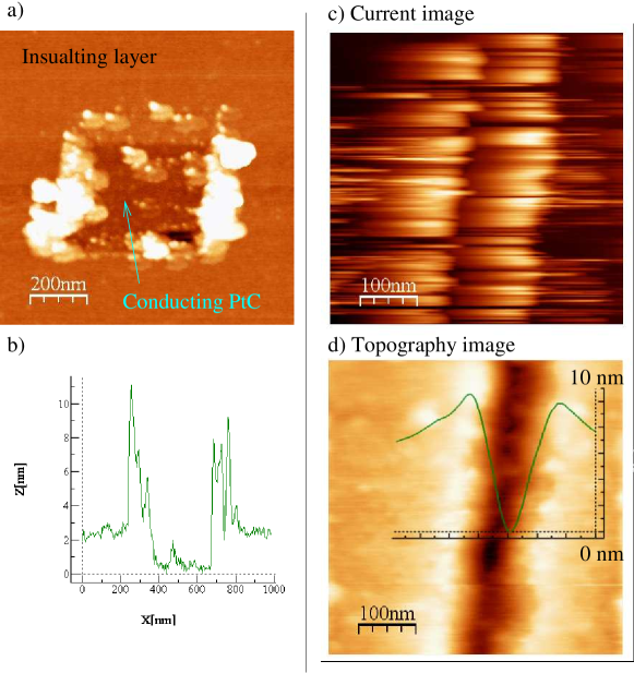
In order to determine experimentally whether electrical contact between DNA and electrodes is possible in our samples we have carried on conducting AFM experiments at the Institute for Electronics, Microelectronics and Nanotechnology (Lille, France) in the group of D. Vuillaume. When we performed conducting AFM scans over the PtC electrodes no current was detected between the tip with a typical bias of and the grounded sample electrodes. The absence of current is probably due to the insulating pentylamine layer between the tip and the electrode surface. To check whether the absence of conduction was due to the insulating pentylamine layer, we scratched the surface in contact mode until conduction appeared probably removing the pentylamine on top of the electrode surface. Once a finite current appeared we switched back to tapping AFM mode and scanned the surface over a wider area. An AFM image obtained during the described experiment is presented on Fig. 30.b. A hole roughly deep was drilled in the region where the substrate was scratched until conductivity appeared. Probably this value provides a measurement of the pentylamine film thickness which in this case also is in the range of a few nanometers.
Conducting AFM data in the bulk of the electrodes indicate that it is very difficult to establish an electrical contact between DNA molecules and the electrodes beneath probably because of the presence of the pentylamine layer. On the edge of the FIB slits however the situation is different. A comparison between conduction (Fig. 30.c) and topography (Fig. 30.d) images in the region of a slit shows that the edge of the gap are not covered by the insulating film and contact is possible in this region. The above images were recorded on a slit from the sample where low temperature conduction properties were investigated in Section VI. They also give a clue on why inverse proximity effect does not occur in the conduction model from Fig. 23 where DNA becomes superconducting due to nanoparticles of diameter although it is deposited on normal electrodes. Indeed even if the molecule rests almost entirely over the normal electrodes, electrical contact can be established only in a region of a few nanometers near the gap.
VIII Conclusions
We first summarize the experimental results obtained in the previous sections.
-
•
Section I describes the DNA solution that was used in all our DNA deposition experiments and showed that it yields satisfactory deposition onto mica.
-
•
Section II shows that binding through DNA extremities allows to deposit molecules on a metallic platinum substrate. No conduction was observed in this case, in agreement with most of other works.
-
•
Section III describes the pentylamine plasma functionalization for the adsorption of DNA molecules. We argued that this technique is reliable only on carbon coated surfaces. When it is applied on mica the pentylamine layer is probably removed at the last step when the sample is dried explaining the absence of DNA molecules on the surface.
-
•
Section IV we demonstrated that reliable combing of DNA molecules across insulating slits can be achieved combining pentylamine and rinsing in a steady flow of water. However the samples we prepared with this technique exhibited insulating behavior for both samples prepared by electron beam lithography and ion beam etching. A possible reason for the absence of conductivity may be that a thin layer of amorphous carbon was evaporated at the last step just before deposition of pentylamine and DNA molecules. While it ensured a good adhesion of pentylamine it could render the edges of the gap insulating by stabilizing the pentylamine even there (see SectionVII). Conducting atomic force microscopy (AFM) measurements could have shown if this explanation is true.
-
•
Section V explains how the gaps for deposition of DNA were fabricated using in situ resistance measurements inside the focused ion beam microscope (FIB). AFM topography of the gaps is also discussed. Starting from this section deposition of DNA molecules was done by D. Klinov.
-
•
Section VI describes electrical transport measurements in the low temperature regime on samples where conduction was established after the deposition of DNA molecules. On four samples superconductivity was observed whereas a last resistive sample had a differential conductance similar to graphene. Due to high critical magnetic fields around we interpreted the observed superconductivity as proximity effect from superconducting nanoparticles inside the FIB slit. On a control sample where a short circuit was formed by stopping FIB etching before the sample became insulating no superconductivity was observed. However a zero bias anomaly was observed, possibly due to the formation of conducting nanofilaments in the gap during the FIB etching. Scanning electron microscope images of the filaments that may be formed are shown on Fig. 24.
-
•
Section VII showed scanning electron microscope (SEM) and AFM images of the gaps. Metallic nanoparticles were identified on the sample from Section VI, they appeared because FIB worked in a special regime on this sample where it disseminated Ga nanoparticles everywhere. On other samples, both metallic filaments and nanoparticles were observed inside the gap. AFM characterization revealed that a carbon contamination layer was deposited by FIB around the gap. We conjectured that this contamination layer was partially graphitic, this probably explains the poor reproducibility of deposition near the slits while good reproducibility was achieved in Section IV. This conjecture also gives insight on the origin of the “graphitic” sample that we measured in Section VI. Due to the limits of AFM resolution on the rough surface of the electrodes, we could not reach a definite conclusion on the presence of DNA molecules around the gaps. Figure 29 shows a few molecules in this region, however DNA was absent in most of our AFM images. Finally both tapping and conducting mode AFM indicate that pentylamine forms an insulating film of a few nanometers on top of the electrode surface. The electrical contact between DNA and electrodes seems possible only at the edges of the slit were conduction was observed in conducting mode AFM.
In conclusion, several arguments can be retained to demonstrate that long range transport across DNA molecules was observed in our experiments. The first argument is statistical, for transport was not observed after deposition of a buffer solution without DNA. However one must be cautious with statistical arguments in these systems where sample to sample fluctuations are large. We note that the conduction in our samples was systematically destroyed when attempts to bond the samples were made even when silver paint was used to avoid uncontrolled voltage spikes across the slits. This observation would be difficult to explain if conduction occured through metalic fillaments only, and suggests a denaturation of the DNA molecules by the solvent from the silver paint. Conduction was also destroyed by UV irradiation with wavelength , however this experiment was performed on only a single sample and more statistics and better control of irradiation doses are needed. Concerning the low temperature transport data, the observed proximity effect suggests that transport takes place across a nanowire with a very small density of states. It is tempting to conclude from this argument that transport indeed takes place along DNA molecules. However here also caution is required since we have shown that FIB can create narrow conducting filaments inside the slits whose properties are not well characterized (for e.g. they seem to exhibit dynamical coulomb blockade). Ultimately one must keep in mind that even if the gaps are about wide on average, transport may actually be probed on a much shorter length-scales around due to the presence of metallic residues. To summarize our experiments provide indications that long range transport in DNA molecules can be achieved through interaction with a disconnected array of metallic nanoparticles, however more systematic investigations are needed to determine the largest lengthscales on which transport can be achieved in this way.
Acknowledgments
We thank F. Livolant, A. Leforestier, D. Vuillaume and D. Deresmes for fruitful discussions. We acknowledge support from ANR QuandADN and DGA. One of us, A.C., acknowledges the support from St Catharine college in Cambridge and to the E. Oppeneheimer foundation.
References
- (1) B. Alberts, D. Bray, A. Johnson, J. Lewis, M. Raff, K. Roberts, P. Walter “Essential Cell Biology” Garland Publishing (1998)
- (2) R.G. Endres, D.L. Cox and R.R.P. Singh, Rev. Mod. Phys. 76, 195 (2004)
- (3) N.C. Seeman, “An overview of structural DNA nanotechnology”, Mol. Biotechnol. 37, 246 (2007)
- (4) P.W.K. Rothemund, Nature 440, 297 (16 March 2006)
- (5) Yu He, Tao Ye, Min Su, Chuan Zhang, Alexander E. Ribbe, Wen Jiang and Chengde Mao, Nature 198, 198 (2008)
- (6) E.S. Andersen, M. Dong, M.M. Nielsen, K. Jahn, R. Subramani, W. Mamdouh, M.M. Golas, B. Sander, H. Stark, C.L.P. Oliveira, J.S. Pendersen, V. Birkedal, F. Besenbacher, K.V. Gothelf and J. Kjems, Nature 459, 73 (2009)
- (7) H.-W Fink and C. Schönenberger, Nature 398 407 (1999)
- (8) M. R. Arkin, E. D. A. Stemp, R. E. Holmlin, J. K. Barton, A. Hoermann, E. J. C. Olson, and P. F. Barbara Science 273, 475 (1996)
- (9) D. B. Hall, R. E. Holmlin, and J. K. Barton, Nature, 382, 731 (1996).
- (10) D. Porath, A. Bezryadin, S. de Vries and C. Dekker, Nature 403 635 (2000)
- (11) A. Yu. Kasumov, M. Kociak, S. Guéron, B. Reulet, V. T. Volkov, D. V. Klinov and H. Bouchiat, Science 291 280 (2001).
- (12) A. Yu. Kasumov, D. V. Klinov, P.-E. Roche, S. Guéron, and H. Bouchiat, App. Phys. Let. 84 1007 (2004);
- (13) A.D. Chepelianskii, D. Klinov, A. Kasumov, S. Guéron, O. Pietrement, S. Lyonnais and H. Bouchiat, New J. Phys. 13, 063046 (2011)
- (14) P.J. de Pablo, F. Moreno-Herrero, J. Colchero, J. Gómez Herrero, P. Herrero, A.M. Baró, Pablo Ordejón, José M. Soler and Emilio Artacho, PRL 85, 4992 (2000)
- (15) A. J. Storm, S. J. T. van Noort, S. de Vries, and C. Dekker, Appl. Phys. Lett. 79, 3881 (2001)
- (16) Y. Zhang, R. H. Austin, J. Kraeft, E. C. Cox and N. P. Ong, PRL 89, 198102 (2002)
- (17) C. Gomez-Navarro, F. Moreno-Herrero, P. J. de Pablo, J. Colchero, J. Gomez-Herrero and A. M. Baro, PNAS 99, 8484 (2002)
- (18) T. Heim, D. Deresmes, and D. Vuillaume, Appl. Phys. Lett. 85, 2637 (2004)
- (19) T. Heim, D. Deresmes, and D. Vuillaume, J. Appl. Phys. 96, 2927 (2004)
- (20) Bingqian Xu, Peiming Zhang, Xiulan Li,and Nongjian Tao, Nano. Let. 4, 1105 (2004)
- (21) Errez Shapir, Hezy Cohen, Arrigo Calzolari, Carlo Cavazzoni, Dmitry A. Ryndyk, Gianaurelio Cuniberti, Alexander Kotlyar, Rosa Di Felice and Danny Porath, Nature Materials 7, 68 (2008)
- (22) Xuefeng Guo, Alon A. Gorodetsky, James Hone, Jacqueline K. Barton and Colin Nuckolls, Nature Nanotechnology 3, 163 (2008)
- (23) M.D. Stoeckenius, J. Biophys. and Biochem. Cytol., 11, 297 (1961)
- (24) P. K. Hansma, J. P. Cleveland, M. Radmacher, D. A. Walters, P. E. Hillner, M. Bezanilla, M. Fritz, D. Vie, H. G. Hansma, C. B. Prater, J. Massie, L. Fukunaga, J. Gurley, and V. Elings, Appl. Phys. Lett. 64, 1738 (1994)
- (25) L. Gross, F. Mohn, N. Moll, P. Liljeroth, G. Meyer, Science 325 1110 (2009)
- (26) H. Tanaka and T. Kawai, Surface Science 539, 531 (2003)
- (27) D. Pastré, O. Piétrement, S. Fusil, F. Landousy, J. Jeusset, M-O David, L. Hamon, E-L. Cam and A. Zozime Biophys. Jour. 85, 2507 (2003)
- (28) Biological Electron Microscopy, Michael J. Dykstra and Laura E. Reuss, Springer (2003) ISBN: 978-0306477492
- (29) J. M. Vargason, K. Henderson and P. Shing Ho, PNAS 98 7265 (2001)
- (30) J. F. Allemand, D. Bensimon, R. Lavery and V. Croquette, PNAS 95 14152 (1998)
- (31) J.F. Allemand, D. Bensimon, L. Jullien, A. Bensimon and V. Croquette Biophis. J. 73 2064 (1997)
- (32) J. Dubochet, M. Ducommun, M. Zollinger and E. Kellenberger J. Ultrastruct. Res. 35 147 (1971)
- (33) M. A. Liberman and A. J. Lichtenberg, “Principles of plasma discharges and materials processing”, A-Wiley interscience publication (1994)
- (34) D. R. Lide, “Handbook of chemistry and physics”, CRC Press 84-th edition (2003), chapters 9-67 and 10-187
- (35) A. Podestà, M. Indrieri, D. Brogioli, G. S. Manning, P. Milani, R. Guerra, L. Finzi and D. Dunlap, Biophysical Journal 89, 2558 (2005)
- (36) A. Bensimon, A. Simon, A. Chiffaudel, V. Croquette, F. Heslot and D. Bensimon, Science 265 2096 (1994)
- (37) P. S. Doyle, B. Ladoux and J.-L. Viovy, Phys. Rev. Lett. 84 4769 (2000)
- (38) L. Angers, F. Chiodi, J. C. Cuevas, G. Montambaux, M. Ferrier, S. Gueron and H. Bouchiat, Phys. Rev. B 77, 165408 (2008)
- (39) A. Yu. Kasumov, R. Deblock, M. Kociak, B. Reulet, H. Bouchiat, I. I. Khodos, Yu. B. Gorbatov, V. T. Volkov, C. Journet and M. Burghard Science 284, 1508 (1999)
- (40) A. Kasumov, M. Kociak, M. Ferrier, R. Deblock, S. Guéron, B. Reulet, I. Khodos, O. Stéphan, and H. Bouchiat Phys. Rev. B 68, 214521 (2003)
- (41) A.Yu. Kasumov, K. Tsukagoshi, M. Kawamura, T. Kobayashi, Y. Aoyagi, K. Senba, T. Kodama, H. Nishikawa, I. Ikemoto, K. Kikuchi, V.T. Volkov, Yu.A. Kasumov, R. Deblock, S. Gueron, and H. Bouchiat Phys. Rev. B 72, 033414 (2005)
- (42) A.Yu. Kasumov, S. Nakamae, M. Cazayous, T. Kawasaki, Y. Okahata Research Letters in Nanotechnology, Article ID 540257 (2009)
- (43) R. E. Bartolo and N. Giordano, Phys. Rev. B 54 3571 (1996)
- (44) P. Joyez, D. Esteve and M.H. Devoret, Phys. Rev. Lett. 80, 1956 (1998)
- (45) M.V. Feigel’man, M.A. Skvortsov and K.S. Tikhonov, Solid State Comun. 149 1101 (2009)
- (46) Orsay physics, private communications
- (47) Jae-Hee Hana, Sun Hong Choia, Tae Young Leea, Ji-Beom Yoo, Chong-Yun Parka, Taewon Jungb, SeGi Yub, Whikun Yic, In Taek Hanb and Jong Min Kimb, Diamond and Related Materials 12, 878 (2003)
- (48) Yuri Lvov, Heinrich Haas, Gero Decher, Helmuth Moehwald and Alexei Kalachev J. Phys. Chem.,97 12835 (1993)
- (49) S. M. Rossnagel, J.J. Cuomo and W.D. Westwood “Handbook of plasma processing technology”, Noyes Publications, Park Ridge U.S.A (1990)
- (50) A. Nabok “Organic and inorganic nanostructures”, Artech House (2005) p. 39