Three-dimensional quantum photonic elements based on single nitrogen vacancy-centres in laser-written microstructures
Abstract
To fully integrate quantum optical technology, active quantum systems must be combined with resonant microstructures and optical interconnects harvesting and routing photons in three diemsnsions (3D) on one chip. We fabricate such combined structures for the first time by using two-photon laser lithography and a photoresist containing nanodiamonds including nitrogen vacancy-centers. As an example for possible functionality, single-photon generation, collection, and transport is successfully accomplished. The single photons are efficiently collected via resonators and routed in 3D through waveguides, all on one optical chip. Our one-step fabrication scheme is easy to implement, scalable and flexible. Thus, other complex assemblies of 3D quantum optical structures are feasible as well.
A fully integrated quantum optical technology requires active quantum systems incorporated into resonant optical microstructures and inter-connected in three dimensions via photonic wires. Nitrogen vacancy-centres (NV-centres) in diamond which are excellent photostable room temperature single-photon emitters Kurtsiefer2000 are ideal candidates for that purpose Jelezko2006 ; Aharonovich2011 . Extensive research efforts to couple NV-centres to photonic structures such as optical microresonators Barclay2009 ; Hausmann2012 , microcavities Wolters2010 ; Sar2011 ; Riedrich-Moller2012 , and waveguides Fu2008 ; Schroder2010 ; Schroder2012 have been pursued. Strategies for integration range from top-down fabrication via etching of diamond membranes Riedrich-Moller2012 ; Hausmann2012 to sophisticated bottom-up assembly of hybrid structures using diamond nanocrystals Wolters2010 ; Sar2011 ; Barclay2009 where the latter approach allows for deterministic coupling. Recently, another approach based on the incorporation of nanodiamonds in soft glass optical fibres via a melting process has been introduced Henderson2011 . Here, we utilize two-photon direct laser writing (DLW) to fabricate fully three-dimensional (3D) structures from a photoresist mixed with a solution of nanodiamonds containing NV-centres. For the first time, this approach facilitates building integrated 3D quantum photonic elements of nearly arbitrary shapes.
On-chip photonic circuits working at the single-quantum level play an important role for future quantum information processing O'Brien2009 . Several approaches to assemble such quantum photonic devices from different fundamental photonic entities have been pursued Benson2011 . For example, by using self-assembled quantum dots in semiconductor membranes, one can exploit the full power of semiconductor nanofabrication technology, and sophisticated structures have been demonstrated O'Brien2009 , even with on-demand coupling architectures Badolato2005 . However, this approach is limited to two-dimensional structures, except for few results obtained by extremely challenging manual membrane-stacking Aoki2008 .
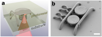
Another easy and low-cost way of fabricating photonic structures is optical lithography via direct laser writing (DLW) kawata2001finer ; deubel2004direct where a tightly focussed femtosecond laser beam is used to expose a photoresist (see Figure 1a). The use of multi-photon absorption enables a sequential 3D exposure by scanning the sample or the focus of the laser. For common negative-tone photoresists, unexposed parts are removed during a development step and the 3D polymer structures remain (see Figure 1b). DLW is well known for the fabrication of photonic crystals deubel2004direct or other photonic elements like resonators liu2010direct ; grossmann2011direct and waveguides Lee2012 . In order to functionalise the structures with optically active material, fluorescent dyes sun2001two , quantum dots Li2006 and metal nanoparticles Shukla2011 have been incorporated. However, until today there has been no 3D structure operating at the fundamental quantum level with single photons from single emitters being collected and routed. Moreover, no combinations of multiple optical elements (different resonators, couplers, waveguides) have been demonstrated. The reason is the lack of photostable quantum emitters which are compatible with the DLW process while still preserving the possibility for high-quality DLW fabrication.
Results
Here, we overcome these obstacles by mixing small amounts of nanodiamonds from solution directly into a known photoresist Fischer2011 (See Methods). This special photoresist allows for the fabrication of transparent optical elements made from an acrylate polymer containing nanodiamonds. The nanodiamonds contain NV-centres which are photostable even after exposure by the DLW laser. After the DLW process they serve as integrated single-photon sources. It is especially noteworthy that our technique is not limited to NV-centres in diamond nanocrystals. It can be applied to any photostable single-photon emitter in nanocrystalline material, e.g. other diamond defect centres, such as Silicon vacancy-centres Neu2011 , or other deep defect centres in large band gap material Weber2010 .
In the following, we demonstrate the fabrication, functionality, and interaction of key building blocks for quantum photonic circuitry. These are interconnects (i.e., waveguides) and functional elements like resonators and emitters. We measure single-photon emission from a diamond nanocrystal in a waveguide-coupled resonator which demonstrates the functional combination of all these building blocks and paves the way to more complex devices.
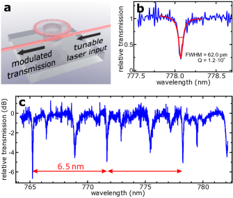
As a first component for integrated photonic circuits, disc resonators with a disc diameter of and a disc thickness of approximately on a stem with diameter were fabricated using the photoresist functionalised with nanocrystals (see Methods). The resonator supports whispering gallery modes which are confined in the disc close to the rim with high quality factors (Q-factors). We measured the Q-factor using a tunable laser coupled into the resonator via a tapered fibreVahala2003 . We found Q-factors as large as at a wavelength of around (see Figure 2 and Methods). The observed free spectral range of of the resonator corresponds well to the expected value of for a disc with diameter derived from geometrical considerations assuming an index of refraction of 1.5.
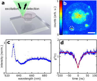
Next, a homebuilt confocal microscope (see Methods) was used to raster scan the fabricated resonator discs (see Figure 3a) and to identify single NV-centres by measuring the second-order autocorrelation function in a Hanbury Brown and Twiss (HBT) interferometer. In parallel, a grating spectrometer was used to resolve the emission spectra of the individual emitters. Figure 3b shows a confocal scan of a resonator where fluorescent defects can be identified as bright spots on the resonator. Encircled is a spot on the resonator’s outer rim where coupling to the disc’s whispering gallery modes is expected. Figure 3d displays an autocorrelation measurement of fluorescence collected from that spot. A clear antibunching dip is observed reaching a value of (standard error) as deduced from the fit shown as red curve. No background correction was applied to these data. This measurement shows that the bright spot indeed corresponds to a single NV-centre in the disc resonator.
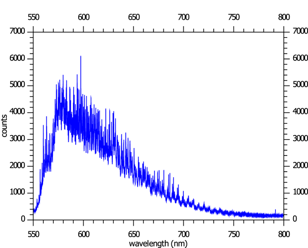
The fluorescence spectrum of an NV-centre at room temperature is typically broadened over from approx. to by phonon sidebands. This corresponds well to the measured emission spectrum shown in Figure 3c. The peak at approximately stems from fluorescence of the photoresist and bleaches after long excitation. For confocal scans and correlation measurements this background light was suppressed by spectral filtering. In addition, there is a fine modulation of the spectrum due to the cavity resonances. It is attributed to photons that were initially emitted into the resonator modes and afterwards scattered out by the diamond nanocrystal. Hence, these photons are detected in addition to the flat unmodulated spectrum emitted directly out of the disc.
As a second photonic element, arc waveguides from the same material with a width of and a length of were built. The waveguides were fabricated close to the disc resonator in order to enable evanescent coupling to the resonator’s modes (see Figure 4a). Their ability to guide light within a broad spectral range is demonstrated by illuminating one end of the waveguide with light from a halogen lamp as seen in Figures 4b and c. The blue and red circular spots correspond to the input and output of the arc waveguide, respectively.
Coupling via the waveguides to the resonator modes was confirmed by shining an excitation laser (wavelength of ) into one port of the waveguide and, after blocking excitation light by a dichroic mirror, analysing the light coming out of the other port. Obviously, the -laser excites background fluorescence in the resonator, which is then coupled back into the waveguide. The measured fluorescence spectrum in Figure 4e thus shows the characteristic modulation by resonator modes and proves a good coupling between guided modes in the arc waveguide and confined modes in the resonator (see Supplementary Information).
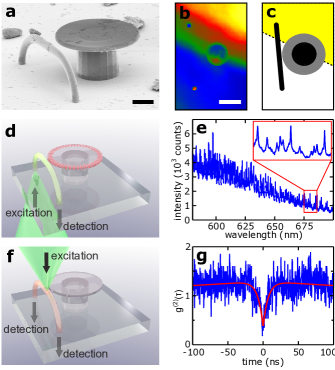
By moving the excitation spot of a second objective over a waveguide (see Figure 4a), individual nanodiamonds inside can be addressed and identified as spots with higher fluorescence. The intensity cross correlation between the waveguide’s two outputs shows a clear antibunching behaviour. This result highlights a way of coupling single emitters to thin waveguides, which can possess very high collection efficiencies, as demonstrated recently using tapered optical fibres Fujiwara2011 ; Schroder2012 . Here, we show a direct on-chip integration of such devices with both waveguide ends accessible. Detection at the waveguide’s ends can yield count rates of after passing a 50/50 beam splitter and spatial and spectral filtering. The autocorrelation function at zero time delay of the fluorescence collected in this way is (standard error) showing the single-photon character of the light (see Figure 4g). When accounting for the 50/50 beam splitter, at high excitation powers the number of background corrected counts from the defect centre is measured to be .
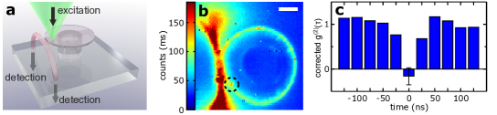
Finally, we verified active quantum functionality of a coupled 3D system, i.e., single photon emission to resonator modes, as well as subsequent collection and routing via a coupled waveguide. In order to do so, raster scans of the excitation spot over the resonator disc were performed while the photons from one of the waveguide’s ends are collected (see Figure 5a). When the excitation laser hits the outer rim of the resonator, the created fluorescence light is coupled to the resonator modes and subsequently out to the waveguide, as can bee seen in Figure 5b. Therefore, the outer rim of the resonator appears bright in the raster image. Bright spots indicate possible positions of NV-centres. To identify NV-centres via their non-classical light emission, an HBT setup, with the laser-written arc waveguide serving as beam splitter, is used. Figure 5b shows this correlation measurement for the NV-centre encircled in Figure 5a. The data shown were acquired with a pulsed laser at repetition rate and background corrected (see Supplementary Information). The value of (standard deviation) is far below the threshold for having equal contributions of two centers and proves that the main contribution to the signal stems from a single NV-centre. This clearly indicates that the NV-centre emits single photons into resonator modes, which are then coupled out and redirected by the arc waveguide. With a single source in a resonator coupled to a waveguide, this device represents a key integrated 3D quantum photonic circuit.
Discussion
In conclusion, we have shown an approach which allows for the direct incorporation of single quantum emitters into true 3D photonic structures of nearly arbitrary shape. The one step fabrication scheme is easy to implement and requires no elaborate clean-room environment. We have pointed out that our method is not limited to NV-centres in nanodiamond, but can be extended to any other stable quantum emitter embedded in nanocrystals. The flexibility of DLW enables immediate scaling-up to more complex structures (see Figure 1b) where single photons are collected, sent through beam splitters, interferometers, or other optical elements inter-connected by waveguides in a 3D architecture. Also tree-dimensional multi-arm quantum interferometers can be implemented. Tuning of individual components, e.g. the resonator, is possible as well (see Supplementary Information). With (partial) metallisation of the structures embedding single photon emitters in 3D plasmonic structures or in metamaterials Rill2008 can be envisioned. A next challenging, but rewarding step is to perform DLW of perfectly aligned 3D structures around emitters of known position. This would enable on-demand fabrication of arbitrary 3D quantum photonic architectures.
Methods
Direct laser writing. The DLW setup consists of a Ti:sapphire oscillator (SpectraPhysics MaiTai HP) delivering pulses centred around . The beam is focussed through an oil-immersion lens (Leica HCX PL APO 100x/1.40-0.70 OIL CS). The sample is moved with a 3D piezo stage (PI P-527.3CL). The writing was performed with average writing power and at scan velocity. The samples were developed in isopropyl alcohol for 30 minutes, afterwards in acetone for 30 minutes, and finally dried super-critically (Leica CPD030).
The new photoresist is based on the monomer pentaerythritol tetraacrylate (PETTA) which contains 350 ppm monomethyl ether hydroquinone as inhibitor. Next, 0.25 % wt of the photoinitiator 7-diethylamino-3-thenoylcoumarin were added. Last, 2 % wt of an ethanol-based nanodiamond suspension were added and stirred overnight. Nanodiamonds were of type 1b and had a median diameter of (Microdiamant AG). Spatial dimensions of the fabricated structures were extracted from scanning electron micrographs.
Confocal microscope. The homebuilt confocal microscope is based on the body of a Zeiss Axiovert 200. Either a frequency doubled Nd:YAG continuous wave laser or a pulsed laser (LDH-P-FA-530, PicoQuant) were used to create the excitation light around . A large-numerical-aperture air microscope objective mounted on a 1D piezo stage (MIPOS 100, piezosystem jena) focussed the excitation light and collected the fluorescence. The sample was scanned by a 2D piezo stage (PXY 80 D12, piezosystem jena). Collected fluorescence light was separated from the excitation laser by a dichroic mirror. Then, it was either spatially filtered and sent to a grating spectrometer or it was spectrally filtered by RG630 glass, split by a 50/50 beam splitter, and directed towards two pinholes. These pinholes could be independently adjusted to spatially filter out different spots of the image plane, so that cross correlations could be measured. After the pinholes the light was directed to avalanche photodiodes (SPCM-AQR-14/SPCM-AQRH-14, Perkin Elmer).
To perform correlation measurements at the waveguide ends, an oil-immersion microscope objective (UPlanSApo 60XO, Olympus) was used for collecting the light, while different air objectives were used to focus the excitation laser onto the sample from the other side. The air objectives were mounted on a 3D piezo system (PXY100 ID and MIPOS 100, piezosystem jena) to enable scanning of the excitation spot while the sample was kept at a fixed position. Also, the 50/50 beam splitter within the HBT setup could be replaced by a D-shaped mirror in an image plane in cases where cross-correlation measurements with high count rates were needed.
Q-factor measurements. The mode structure of the disc resonators was analysed by means of coupling in a tunable external-cavity diode laser (Velocity Series, New Focus) at around via the evanescent fields of a tapered optical fibre. By tuning the frequency of the laser over the distinct whispering gallery modes, light was coupled into the resonator and different modes could be observed as Lorentzian shaped dips in the transmitted power. The polarization of the incoming light was chosen to maximize the coupling depth. For normalizing the data sets, we first performed a reference scan with an uncoupled fibre taper and compared the results to the situation when the same taper was coupled to the resonator. This provided direct access to the different coupling depths and cancelled out overlaying power modulations caused by slightly non-adiabatic taper transitions.
The Q-factors were calculated from the dips by a Lorentzian fit function with an additional linear term to better match the local environment of the resonances. The fibre taper used had a waist diameter of . Measurements were performed in full contact.
Acknowledgements
The Berlin team acknowledges support by DFG (FOR1493 and SFB951). The Karlsruhe team acknowledges support by the DFG-Center for Functional Nanostructures (CFN) via subprojects A1.4 and A1.5 and by the Karlsruhe School of Optics & Photonics (KSOP). J.W. acknowledges funding by the state of Berlin (Elsa-Neumann).
Author contributions
A.W.S. wrote the manuscript and conceived the experiment with J.F., J.K. and J.F. produced the samples, A.W.S., R.H. and J.W. performed the optical measurements and data analysis. M.W. and O.B. supervised the study. All authors discussed the experiment, the results and the manuscript.
Additional Information
The authors declare no competing financial interests.
References
- (1) Kurtsiefer, C., Mayer, S., Zarda, P., and Weinfurter, H. Stable solid-state source of single photons. Phys. Rev. Lett. 85, 290–293, (2000).
- (2) Jelezko, F. and Wrachtrup, J. Single defect centres in diamond: A review. Phys. Stat. Sol. (a) 203, 3207–3225 (2006).
- (3) Aharonovich, I. et al. Diamond-based single-photon emitters. Rep. Prog. Phys. 74, 076501 (2011).
- (4) Barclay, P. E., Santori, C., Fu, K.-M., Beausoleil, R. G., and Painter, O. Coherent interference effects in a nano-assembled diamond nv center cavity-qed system. Opt. Express 17, 8081–8097, (2009).
- (5) Hausmann, B. J. M. et al. Integrated diamond networks for quantum nanophotonics. Nano Lett. 12, 1578–1582 (2012).
- (6) Wolters, J. et al. Enhancement of the zero phonon line emission from a single nitrogen vacancy center in a nanodiamond via coupling to a photonic crystal cavity. Appl. Phys. Lett. 97, 141108 (2010).
- (7) van der Sar, T. et al. Deterministic nanoassembly of a coupled quantum emitter–photonic crystal cavity system. Appl. Phys. Lett. 98, 193103 (2011).
- (8) Riedrich-Möller, J. et al. One- and two-dimensional photonic crystal microcavities in single crystal diamond. Nature Nano. 7, 69–74, January (2012).
- (9) Fu, K.-M. C. et al. Coupling of nitrogen-vacancy centers in diamond to a gap waveguide. Appl. Phys. Lett. 93, 234107 (2008).
- (10) Schröder, T., Schell, A. W., Kewes, G., Aichele, T., and Benson, O. Fiber-integrated diamond-based single photon source. Nano Lett. 11, 198–202, (2011).
- (11) Schröder, T. et al. A nanodiamond-tapered fiber system with high single-mode coupling efficiency. Opt. Express 20, 10490–10497 (2012).
- (12) Henderson, M. R. et al. Hybrid materials: Diamond in tellurite glass: a new medium for quantum information. Adv. Mater. 23, 2772–2772 (2011).
- (13) O’Brien, J. L., Furusawa, A., and Vuckovic, J. Photonic quantum technologies. Nature Photon. 3, 687–695 (2009).
- (14) Benson, O. Assembly of hybrid photonic architectures from nanophotonic constituents. Nature 480, 193–199 (2011).
- (15) Badolato, A. et al. Deterministic coupling of single quantum dots to single nanocavity modes. Science 308, 1158–1161 (2005).
- (16) Aoki, K. et al. Coupling of quantum-dot light emission with a three-dimensional photonic-crystal nanocavity. Nature Photon. 2, 688–692 (2008).
- (17) Kawata, S., Sun, H. B., Tanaka, T., and Takada, K. Finer features for functional microdevices. Nature 412, 697–698 (2001).
- (18) Deubel, M. et al. Direct laser writing of three-dimensional photonic-crystal templates for telecommunications. Nature Mater. 3, 444–447 (2004).
- (19) Liu, Z. P. et al. Direct laser writing of whispering gallery microcavities by two-photon polymerization. Appl. Phys. Lett. 97, 211105–211105 (2010).
- (20) Grossmann, T. et al. Direct laser writing for active and passive high-q polymer microdisks on silicon. Opt. Express 19, 11451–11456 (2011).
- (21) Lee, C.-W., Pagliara, S., Keyser, U., and Baumberg, J. J. Perpendicular coupling to in-plane photonics using arc waveguides fabricated via two-photon polymerization. Appl. Phys. Lett. 100, 171102 (2012).
- (22) Sun, H., Tanaka, T., Takada, K., and Kawata, S. Two-photon photopolymerization and diagnosis of three-dimensional microstructures containing fluorescent dyes. Appl. Phys. Lett. 79, 1411 (2001).
- (23) Li, J., Jia, B., Zhou, G., and Gu, M. Fabrication of three-dimensional woodpile photonic crystals in a PbSe quantum dot composite material. Opt. Express 14, 10740–10745 (2006).
- (24) Shukla, S. et al. Subwavelength direct laser patterning of conductive gold nanostructures by simultaneous photopolymerization and photoreduction. ACS Nano 5, 1947–1957 (2011).
- (25) Fischer, J. and Wegener, M. Three-dimensional direct laser writing inspired by stimulated-emission-depletion microscopy. Opt. Mater. Express 1, 614–624 (2011).
- (26) Neu, E. et al. Single photon emission from silicon-vacancy colour centres in chemical vapour deposition nano-diamonds on iridium. New J. Phys. 13, 025012 (2011).
- (27) Weber, J. R. et al. Quantum computing with defects. P. Natl. Acad. Sci. 107, 8513–8518 (2010).
- (28) Vahala, K. J. Optical microcavities. Nature 424, 839–846 (2003).
- (29) Fujiwara, M., Toubaru, K., Noda, T., Zhao, H.-Q., and Takeuchi, S. Highly efficient coupling of photons from nanoemitters into single-mode optical fibers. Nano Lett. 11, 4362–4365 (2011).
- (30) Spagnolo, N. et al. Quantum interferometry with three-dimensional geometry. Sci. Rep. 2, 862 (2012).
- (31) Rill, M. S. et al. Photonic metamaterials by direct laser writing and silver chemical vapour deposition. Nature Mater. 7, 543–546 (2008).
Spectral mode analysis
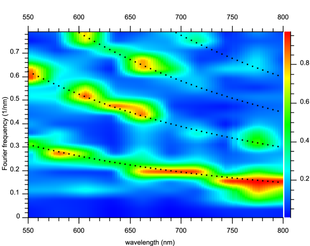
For a quantitative analysis of the spectrum measured from the background fluorescence by a grating spectrometer (see Figure 6) we performed a segmented Fourier transformation on the data. We divided the set into wide segments and performed numerical fast Fourier transformations on each of them individually. Afterwards we matched the frequency amplitude ranges by normalizing the different segments to each other, colour coded the resulting profiles, and merged the different wavelength ranges to obtain the plot shown in Figure 7. The different Fourier components of the resonator’s whispering gallery modes (WGMs) are clearly visible as bands evenly spaced by an integer multiple of the lowest observable base frequency. This frequency component is directly related to 1/FSR and corresponds well with the theoretical estimated value based on the size of the discs. The black dotted lines are fits to this value and its different higher-order multiples.
Tuning of the Resonators
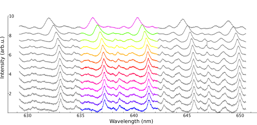
Figure 8 shows the tuning of a resonator under vacuum conditions. To tune the resonator, a laser was focussed on its rim. The spectra shown were acquired from bottom to top in equal timesteps of . After some steps the mode begins to shift. Laser induced shifts of the resonance of resonators were previously observed by us Wolters2010_ and others Others . Its physical or chemical origin is not understood yet, but it is assumed to be caused by a modification of the resonator’s local shape or a change of the index of refraction of the resonators material. It is worth noting that tuning of the resonator is possible even without oxygen present.
This is a very important feature, since it enables tuning of the resonator’s whispering gallery modes to the zero phonon lines of the nitrogen vacancy centres. Since no oxygen is needed for this procedure, it can be used in a cryostat at low temperatures. In addition to the possibility of tuning the resonances to lines of the optical emitters, it would be also possible to match resonances of different resonators and achieve controlled coupling among them.
Background correction
In the case of continuous excitation of an emitter with intensity , second order correlation functions and the quantum mechanically uncorrelated background of the intensity with , the joint second order correlation function is given by:
| (1) |
By knowing the intensities and it one can calculate the function of the bare emitter from a measurement of the joint correlation function .
In case of pulsed excitation this background correction is more complicated, since the emission of emitter and background are correlated by the excitation laser. This problem can be avoided by only looking at time intervals corresponding to one laser period. In the analysis of an experiment’s -data acquired with a Hanbury Brown and Twiss setup, this can be achieved by binning together all events in the time windows , with the laser repetition time ( in our experiment) and being an integer.
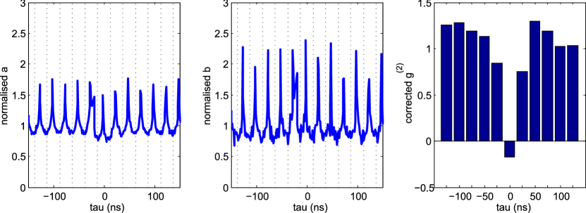
Figure 9 a and b show the normalised coincidence counts measured with pulsed excitation at the location of an NV centre at the resonator’s rim (in a)) and at a location without an NV center next to it also on the rim (in b)), respectively. Thus the data in figure 9a) corresponds to coincidences from signal and background whereas figure 9b) represents the background coincidences only. Binning to intervals of was performed for better visibility. Normalisation was done by averaging for long times ( over 256 periods), where contributions from the NV centre’s bunching behaviour are negligible. Also the photons normally missed in an HBT like start-stop configuration were taken into account. A comparison of the background photons rate with the intensity of the combined signal gave and , equivalent to a background to signal ratio of 2. Figure 9 c shows the resulting corrected function, with bins sizes corresponding to the laser repetition time.
For zero time delay . The error bar for this value stems from three contribution, with the main contribution stemming from the uncertainties in the ratio , which we assumed to be 10 % (). This error is due to the fact that background and signal were measured at neighboring positions on the resonator’s rim, but not at the same one (see Figure 5 b of the main text, ). The other two contributions are the statistical variations in the photon number for the zero time delay bin, which were both assumed to be Possonian ( and ). This results in an error of after adding the contributions via Gaussian error propagation.
References
- (1) Wolters, J. et al. Enhancement of the zero phonon line emission from a single nitrogen vacancy center in a nanodiamond via coupling to a photonic crystal cavity. Appl. Phys. Lett. 97, 141108 (2010).
- (2) Lee, H. S. et al. Local tuning of photonic crystal nanocavity modes by laser-assisted oxidation. Appl. Phys. Lett. 95, 191109 (2009).