Effect of plasma resonances on dynamic characteristics of double graphene-layer optical modulator
Abstract
We analyze the dynamic operation of an optical modulator based on double graphene-layer(GL) structure utilizing the variation of the GL absorption due to the electrically controlled Pauli blocking effect. The developed device model yields the dependences of the modulation depth on the control voltage and the modulation frequency. The excitation of plasma oscillations in double-GL structure can result in the resonant increase of the modulation depth, when the modulation frequency approaches the plasma frequency, which corresponds to the terahertz frequency for the typical parameter values.
I Introduction
The gapless energy spectrum of graphene layers (GLs)) 1 , results in the interband absorption of the electromagnetic radiation from the terahertz to ultraviolet range2 . This opens up prospects to use graphene structures in active and passive optoelectronic devices. Novel lasers, photodetectors, modulators, and mixers have been proposed and studied 3 ; 4 ; 5 ; 6 ; 7 ; 8 ; 9 ; 10 ; 11 ; 12 ; 13 ; 14 ; 15 (see also the review paper 16 and references therein). Varying the controlling voltage one can effectively change the electron and hole densities and the Fermi energy and, hence, the intraband and interband absorption in GLs. An increase in the electron (hole) density increases the intraband absorption (associated with the Drude mechanism), but it decreases the interband absorption due to the Pauli blocking effect. Which mechanism dominates depends on the incident photon energy and the momentum relaxation time of electrons and holes, . At the frequencies of infrared and visible radiation, , so that the Drude absorption is weak. Even in the terahertz (THz) range, the latter inequality can be valid for high quality GLs (like those studied in Refs. 17 ; 18 ), even at room temperatures.
In this paper, we develop a device model of a double-GL optical modulator proposed and demonstrated in Ref. 19 . In this modulator, GLs were separated by relatively thick barrier and the structure was integrated with an optical waveguide The operation of the device under consideration is associated with the filling of GLs with electrons and holes injected from the contacts under the self-consistent electric field created by the applied voltage and the electron and hole charges in GLs. This process determines both static and dynamic characteristics of the double-GL modulator. At the non-stationary conditions, the dynamics of the electron-hole plasma in double-GL can exhibit resonant response due to the excitation of plasma oscillations similar to those well known in more traditional two-dimensional electron and hole systems 20 ; 21 ; 22 ; 23 ; 24 ; 25 ; 26 ; 27 ; 28 ; 29 ; 30 . The plasma oscillations in GL-structures also were considered previously (see, for instance, Refs. 31 ; 32 ; 33 ; 34 ; 35 ). A resonant plasmonic THz using double-GL structures was recently studied in Ref. 36 .
In this paper, we develop a device model for double-GL modulators of optical radiation and demonstrate that the resonant excitation of plasma oscillations in double-GL modulators can provide an efficient modulation of optical radiation by high frequency signals, in particular, in the THz range.
The variation of the Fermi energy in double-GL is associated with the electron and hole injection and extraction by the side contacts. Therefore, the consideration of the electron-hole plasma dynamics in double-GLs must account for the self-consistent electric field found from the solution of the hydrodynamic equations and the Poisson equation.
II Equations of the model
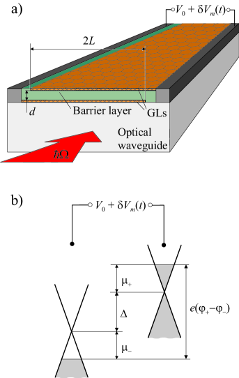
We consider the double-GL modulator reported in Ref. 19 . Its simplified structure is shown in Fig. 1(a). We assume that each GL is connected to one side contact and is isolated from the opposite contact (connected to the other GL), The voltage, , applied between these contacts, , where and are the bias and modulation components. We set , where is the modulation frequency. The latter is much smaller than the frequency of the incident optical radiation : . The system of two highly conducting side contacts can be considered as a slot line enabling the propagation of the modulation signals. The side contacts can also be connected to or be a part of THz antenna, which converts the incoming THz radiation into the modulation voltage.
The absorption coefficient of the light wave propagating along the waveguide with double-L on topGL is determined by the real part of the double-GL conductivity at the frequency :
| (1) |
where is the speed of light in vacuum and is the dielectric constant of the waveguide material. The symbol means the averaging accounting for the distribution of the optical field in the waveguide, where the -axis and -axis correspond to the direction along double-GL structure and perpendicular to the -axis corresponding to the direction of the wave propagation direction in the waveguide. Thus,
| (2) |
where
is the mode overlap factor and is the GL length, which is approximately equal to the spacing between the side contacts as shown in Fig. 1(a).
We assume that the electron and hole momentum relaxation time is associated with the scattering due to disorder and acoustic phonons, so that its energy dependence is given by , where is the characteristic scattering frequency at (at the Dirac point). In this case, the real part of the conductivity of two GLs at can be presented as 10
| (3) |
Here and are the GL Fermi energies counted from the Dirac point in the upper and lower GLs, respectively, is the temperature, and is the electron charge. The first five terms in Eq. (4) correspond to the contributions of the interband transitions to the conductivity of the upper and lower GLs. These terms explicitly account for the Pauli blocking effect. The last term in Eq. (3) accounts for the intraband transitions. It is presented in the form providing an interpolated dependence of the intraband conductivity on the Fermi energies and the temperature. At slow variation of the applied voltage, , where obeys the following equation:
| (4) |
The quantity is determined by the electric field between GLs and the thickness of the barrier layer between GLs . Generally speaking (at sufficiently fast variations of the voltage), the spatial distributions of the electron and hole densities do not follow the variation of the applied voltage, and the Fermi energies depend on the coordinate : and .
The Fermi energies in GLs are governed by the following equation:
| (5) |
where cm/s is the characteristic velocity of electrons and holes in GLs. Since the spacing, , between GLs is rather small compared to , one can use the following formulas which relate the densities and the electric potentials of GLs :
| (6) |
The negative values of correspond to the case when a GL is filled by electrons, whereas the positive values correspond to the filling by holes.
III Modulation characteristics
When the control voltage varies slowly, one can set
| (7) |
and, hence,
| (8) |
where is governed by the following equation:
| (9) |
Here
| (10) |
If nm, (Al2O3), and K, from Eq.(10) we obtain mV.
At sufficiently large bias voltage , the electron and hole systems in GLs become degenerate (i.e., ), and Eq. (10) yields
| (11) |
so that, taking into account Eq. (4),
| (12) |
Using Eqs. (1) and (3) and considering Eq. (8), we arrive at the following formula for the absorption coefficient:
| (13) |
Here
| (14) |
is the characteristic collision frequency of electrons and holes (which is assumed to be proportional to ), and is the fine structure constant, (so that ).
In the near infrared range of frequencies, , the contribution of the intraband absorption at low control voltages is small. This implies that the last term in the right-hand side of Eq. (13) is much smaller than unity.
Considering a modulator for optical radiation with the wavelength nm () eV as in Ref. 19 , setting eV, mV, and s-1, we obtain that the last term in Eq. (13) is about 0.03. Thus, in the case of even modestly perfect GLs, this term is relatively small and can be omitted. This implies that in such a case, the modulation is primarily due to the voltage control of the Pauli blocking but not due to the variations of the intraband absorption.
In the most realistic case , the ratio of the intensities of output (modulated by slow varying voltage) and input radiation, and , respectively, taking into account that the second and fourth terms yield the same contribution and omitting the third and fifth terms in Eq. (14), can be presented as
| (15) |
where is the double-GL length in the direction of radiation propagation. and . Equation (15) describes the variation of the output radiation caused by relatively slow variations of the applied voltage with arbitrary swing. Using Eq. (15), one can estimate the modulation depth and the extinction ratio for the case of relatively slow modulation and when varies from to , where : and .
IV Small signal linear modulation characteristics
We now assume that is sufficiently large to form the degenerate electron and hole systems in the pertinent GLs, while the time dependence of is still characterized by a small modulation frequency. In this case, from Eq. (15) we obtain the following formulas of the modulation amplitude and the modulation depth of the output radiation :
| (16) |
and
| (17) |
where .
In particular, at , when reaches a maximum, Eqs. (16) and (17) yield respectively
| (18) |
| (19) |
V Plasma oscillations in double-GL structures
In the double-GL structures with sufficiently high conductivity at low modulation frequencies, one can use Eq. (6), i.e., put . However, at elevated modulation frequencies (for instance, in the THz range), the spatial distributions of the ac components of the electron and hole charges, the electron and hole Fermi energies, and the self-consistent electric potential are nonuniform because these distributions do not follow fast modulation signals. In sufficiently perfect GLs, the modulation signals can excite the electron-hole plasma oscillations. In this situation, the ratio of the ac component of the radiation intensity to the input intensity is given by the following equation, which replaces Eq. (16):
| (20) |
The last factor in the right-hand side of Eq. (20) accounts for the contributions of different parts of GLs being dependent on local values of the Fermi energies and, hence, the local values of the ac potentials [see Fig. 1(b)].
To find the distributions of and , one can use a system of hydrodynamic equations (Euler equation and continuity equation) adjusted to the features of the electron and hole spectra in GLs 35 ) for the electron and hole plasmas in the upper and lower GLs coupled with the Poisson equation. For simplicity, we use the Poisson equation in the gradual-channel approximation, which leads to Eq. (6) above. The linearized versions of the equations in question can be reduced to the following equation for the ac component of the potential at the frequency 36 :
| (21) |
| (22) |
Here is the collision frequency of electrons in GLs with impurities and acoustic phonons and is the characteristic velocity of plasma waves in GLs. Since electrons and holes belong to different GLs separated by the rather high and thick barrier, their mutual collisions can be neglected. The plasma-wave velocity is determined by the net dc electron and hole density (i.e., by the Fermi energy) and the gate layer thickness 31 ; 33 ; 35 : , where is the coupling constant (). Similar equations were obtained for the gated electron channels in the traditional heterostructures. The difference is in the existence of two interacting channel and in different values of . At nm and eV, one obtains .
The plasma wave velocity in GL system is much higher than that in the standard gated channels 34 ; 35 . Large values of in the double-GL should allow us to achieve rather high plasma frequencies (in the THz range) in the devices with relatively large values of (in the micrometer range). If the left-side contact and the upper GL and the right-side contact and the lower GL, see Fig. 1(a)] are are very close 32 , one can disregard the gaps between GLs and the contacts and use the following boundary conditions for Eqs. (21) and (22):
| (23) |
| (24) |
The latter boundary condition reflects the fact that the electron and hole currents are equal to zero at the disconnected edges of GLs (at in the upper GL and at in the lower GL)
Fist from Eqs. (21) and (22) we obtain
| (25) |
where is a constant. Considering Eq. (25), Eqs. (21) and (22) can be presented as
| (26) |
| (27) |
Solving Eqs. (26) and (27) with boundary conditions (24) and (25), we obtain
| (28) |
| (29) |
Here . Introducing the characteristic plasma frequency , one obtains .
In the low modulation frequency limit (when , where is the Maxwell relaxation time, and, hence, ), one obtains and , i.e., the spatial distribution of the ac potential across the GLs is flat.
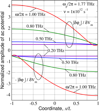
Figure 2 shows examples of the spatial distributions of the amplitudes of the ac potential across GLs, calculated for different modulation frequencies using Eqs. (28) and (29). As seen from Fig. 2, the amplitudes and are close to the amplitude of the applied ac voltage at relatively low modulation frequencies ( and 0.5 THz). However, with increasing , the amplitudes dramatically increase (see the curves corresponding to and 1.00 THz). This is attributed to the excitation of plasma oscillations whose amplitude grows as the modulation frequency approaches to the plasma resonance frequency (see below).
VI Resonant modulation
Substituting and from Eqs. (28) and (29) into Eq. (21) and integrating over , we obtain
| (30) |
yielding for the normalized modulation depth:
| (31) |
Using Eq. (31), the normalized modulation depth can also be expressed via the characteristic plasma frequency :
| (32) |
At , Eq. (32) yields
| (33) |
Equations (19) and (33) provide the dependences of the modulation depth on the structural parameters and the modulation frequency (particularly the frequency dependenceat the roll-off) obtained experimentally and described in Ref. 19.
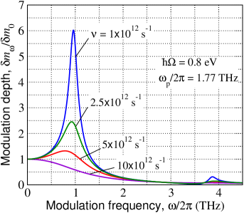
The character of the dependence of the modulation depth on the modulation frequency depends on the collision frequency . Figure 3 shows the frequency dependences (on ) of the normalized modulation depth calculated using Eq. (32) for devices with different values of the collision frequency . It is assumed that the plasma frequency THz. For the characteristic plasma velocities cm/s (as in the estimate in the previous section), this frequency corresponds to m, i.e., to the length of GLs (size of the waveguide) close to the optical wavelength under consideration.
At relatively large collision frequencies , the modulation depth monotonically decreases with increasing the modulation frequency [in line with Eq. (33)]. The curve for s-1 in Fig. 3 corresponds to s and the 3dB roll-off frequency THz. In the devices with a smaller , i.e., with a smaller plasma-wave velocity, , or larger length of GLs, , the Maxwell relaxation time is longer, so that the roll-off frequency is smaller. However, in the devices with relatively small , can exhibit a steep increase when approaches to the plasma resonance frequency. The sharpness of the modulation depth peak and its height rise with decreasing (i.e., with an increasing quality factor of the plasma resonances, ). This also seen in Fig. 4 (compare the solid and dashed lines).
The plasma resonance frequencies, . Here is the resonance index. As can be derived from Eq. (32), the resonance frequencies are given by the solution of the following equation:
| (34) |
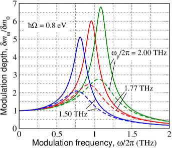
Equation (34), in particular, yields , so that at THz, one obtains THz. The second (even) resonance corresponds to THz. Thus, apart from a pronounced first resonance, a fairly weak second resonance is also seen in Fig.3. A characteristic plasma frequency falls in the THz range. As seen in Fig. 4, an increase in and, consequently, in shifts the positions of the peaks in the frequency dependence of the modulation depth. However, this shift can not be used for the electrical control because the bias voltage corresponds to the energy of photons of modulated radiation. This is in contrast to other THz voltage-controlled devices using the resonant excitation of plasma oscillations (see, for instance, Ref. 36 ).
VII Conclusions
In summary, we developed a device model for an optical modulator based on the double-GL structure that was recently proposed and experimentally realized 19 . The double-GL modulator utilizes the variation of absorption due to the electrically controlled Pauli blocking effect. Our model accounts for the interband and intraband absorption and the plasma effects in GLs determining the spatio-temporal distributions of the electron and hole densities and the absorption coefficient, The developed model yields the dependence of the modulation depth on the control voltage for strong but slow modulation signals and for small-signal modulation in a wide range of frequencies. The dependence of the modulation depth on the modulation frequency is determined by the relationship between the collision frequency of electrons and holes and the characteristic plasma frequency (or between the latter and the Maxwell relaxation time). At relatively large collision frequencies (or small plasma frequencies), the modulation depth is a monotonically decreasing function of the modulation frequency. The obtained dependencies qualitatively explain the experimental results. However, we predict that in the double-GL structures with relatively weak disorder and, hence, with a low collision frequencies, and a sufficiently high quality factor of the plasma oscillations, the modulation depth exhibits a sharp maximum at the modulation frequency, which corresponds to the plasma resonance. The frequency of the latter falls in the THz range for typical parameter values. This opens up the possibility to use the double-GL structures for effective modulation of optical radiation by THz signals.
Acknowledgments
This work was supported by the Japan Science and Technology Agency, CREST, The Japan Society for promotion of Science, Japan, and TERANO-NSF grant. The work at RPI was supported by the US National Science Foundation and EAGER program (monitored by Dr. Usha Varshne).
References
- (1) A. H. Castro Neto, F. Guinea, N. M. R. Peres, K. S. Novoselov, and A. K. Geim, Rev. Mod. Phys. 81, 109 (2009).
- (2) J. M. Davlaty, S. Shivaraman, J. Strait, P. Geotge, M. Chandrashekhar, F. Rana, M. G. Sprncer, D. Veksler, and Y. Chen, Appl. Phys. Lett.93, 131905 (2008).
- (3) V. Ryzhii, M. Ryzhii, and T. Otsuji, J. Appl. Phys. 101, 083114 (2007).
- (4) M.Ryzhii and V.Ryzhii, Jpn. J. Appl. Phys. (Express Lett.) 46, L151 (2007).
- (5) F. Rana, IEEE Trans. Nanotechnol. 7, 91 (2008).
- (6) V.Ryzhii, M.Ryzhii, and T.Otsuji, Phys. Stat. Sol. (c) 5, 261 (2008).
- (7) A. Satou, F. T. Vasko, and V. Ryzhii, Phys. Rev. B 78, 115431 (2008).
- (8) A. A. Dubinov, V. Ya. Aleshkin, M. Ryzhii, T. Otsuji, and V. Ryzhii, Appl. Phys. Express 2, 092301 (2009).
- (9) V. Ryzhii, M. Ryzhii, A. Satou, T. Otsuji, A. A. Dubinov, and V. Ya. Aleshkin, J. Appl. Phys. 106, 084507 (2009)
- (10) V. Ryzhii, A. A. Dubinov, T. Otsuji,V. Mitin, and M.S.Shur, J. Appl. Phys. 107, 054505 (2010).
- (11) V. Ryzhii, V. Mitin, M. Ryzhii, N. Ryabova, and T. Otsuji, Appl. Phys. Express 1, 063002 (2008).
- (12) V. Ryzhii and M. Ryzhii, Phys. Rev. B 79, 245311 (2009).
- (13) F. Xia, T. Mueller, Y-M. Lin, A. Valdes-Garsia, and F. Avouris, Nature Nanotecnology, 4, 839 (2009).
- (14) T. Mueller, F. Xia, and and F. Avouris, Nature Photon., 4, 297 (2010).
- (15) X.D.Xu, N.M.Gabor, J.S.Allen, A.M. van der Zande, and P.L.McEuen, Nano Lett., 10, 562 (2010).
- (16) F. Bonaccorso, Z. Sun, T. Hasa, and A.C. Ferrari, Nat. Photonics, 4, 611 (2010).
- (17) P. Neugebauer, M. Orlita, C. Faugeras, A.-L. Barra, and M. Potemski, Phys. Rev. Lett. 103, 136403 (2009).
- (18) M. Orlita and M. Potemski, Semicond. Sci. Technol. 25, 063001 (2010).
- (19) M. Liu, X. Yin, and X. Zhang, Nano Lett. 12, 1482 (2012)
- (20) S. J. Allen, Jr., D. C. Tsui, and R. A. Logan, Phys. Rev. Lett. 38, 980 (1977).
- (21) D. C. Tsui, E. Gornik, and R. A. Logan, Solid State Commun. 35, 875 (1980).
- (22) M. Dyakonov and M. Shur, IEEE Trans. Electron Devices 43, 1640 (1996).
- (23) W. Knap, Y. Deng, S. Rumyantsev, J.-Q. Lu, M. S. Shur, C. A. Saylor, and L. C. Brunel, Appl. Phys. Lett. 80, 3433 (2002).
- (24) X. G. Peralta, S. J. Allen, M. C. Wanke, N. E. Harff, J. A. Simmons, M. P. Lilly, J. L. Reno, P. J. Burke, and J. P. Eisenstein, Appl. Phys. Lett. 81, 1627 (2002).
- (25) T. Otsuji, M. Hanabe and O. Ogawara, Appl. Phys. Lett. 85, 2119 (2004).
- (26) J. Lusakowski, W. Knap, N. Dyakonova, L. Varani, J. Mateos, T. Gonzales, Y. Roelens, S. Bullaert, A. Cappy and K. Karpierz, J. Appl. Phys. 97, 064307 (2005).
- (27) F. Teppe, W. Knap, D. Veksler, M. S. Shur, A. P. Dmitriev, V. Yu. Kacharovskii, and S. Rumyantsev, Appl. Phys. Lett. 87, 052105 (2005).
- (28) V.Ryzhii, A.Satou, W.Knap, and M.S.Shur. J. Appl. Phys. 99, 084507 (2006).
- (29) A. El Fatimy, F. Teppe, N. Dyakonova, W. Knap, D. Seliuta, G. Valusis, A. Shcherepetov, Y. Roelens, S. Bollaert, A. Cappy, and S. Rumyantsev, Appl. Phys. Lett. 89, 131926 (2006).
- (30) J. Torres, P. Nouvel, A. Akwaoue-Ondo, L. Chusseau, F. Teppe, A. Shcherepetov, and S. Bollaert, Appl. Phys. Lett.89, 201101 (2006)
- (31) V. Ryzhii, Jpn. J. Appl. Phys. 45, L923 (2006).
- (32) O. Vafek, Phys. Rev. Lett. 97,266406 (2006).
- (33) L. A. Falkovsky and A. A. Varlamov, Eur. Phys. J. B 56, 281 (2007)
- (34) V. Ryzhii, A.Satou, and T. Otsuji, J. Appl. Phys. 101 ,024509 (2007).
- (35) D. Svintsov, V. Vyurkov, S. Yurchenko, T. Otsuji, and V. Ryzhii, J. Appl. Phys. 111, 083715 (2012).
- (36) V. Ryzhii, T. Otsuji, M. Ryzhii, and M. S. Shur, J. Phys. D: Appl. Phys. 45, 302001 (2012).