Valley polarized quantum Hall effect and topological insulator phase transitions in silicene
Abstract
The electronic properties of silicene are distinct from both the conventional two dimensional electron gas and the famous graphene due to strong spin orbit interaction and the buckled structure. Silicene has the potential to overcome limitations encountered for graphene, in particular the zero band gap and weak spin orbit interaction. We demonstrate a valley polarized quantum Hall effect and topological insulator phase transitions. We use the Kubo formalism to discuss the Hall conductivity and address the longitudinal conductivity for elastic impurity scattering in the first Born approximation. We show that the combination of an electric field with intrinsic spin orbit interaction leads to quantum phase transitions at the charge neutrality point, providing a tool to experimentally tune the topological state. Silicene constitutes a model system for exploring the spin and valley physics not accessible in graphene due to the small spin orbit interaction.
The quantum Hall effect (QHE) is one of the most striking phenomena in the field of condensed matter physics since its discovery in the 1980s 1 . It is referred to as integer quantum Hall effect as the Hall conductivity takes values of with an integer . The QHE in two dimensional electron gases is of particular interest. Recently, the experimental realization of graphene, a stable monolayer of carbon atoms 2 ; 3 , has stimulated additional interest in two dimensional systems 4 ; 5 . Graphene exhibits quantized conductivity values of , . Among the unusual transport properties, the quantum spin Hall effect is particularly exciting as it constitutes a new phase of matter 6 ; 7 . It requires strong spin orbit interaction (SOI) but not an external perpendicular magnetic field. When Kane and Mele 6 in a ground breaking study of graphene had proposed a new class of insulators, the topological insulators (TIs), great experimental and theoretical excitement was generated 8 ; 9 ; 10 ; 11 ; 12 ; 13 . In addition to the quantum spin Hall effect, an analogous quantum valley Hall effect 14 ; 15 arises from a broken inversion symmetry, where Dirac fermions in different valleys flow to opposite transverse edges when an in-plane electric field is applied in the presence of intrinsic SOI. The quantum valley Hall effect paves the way to electric generation and detection of valley polarization. Since the occurrence of conducting surface states in TIs is related to the SOI 12 and SOI is also a crucial criterion for the quantum spin Hall effect, it has been proposed to search for new materials with strong SOI for application in spintronic devices 6 ; 12 .
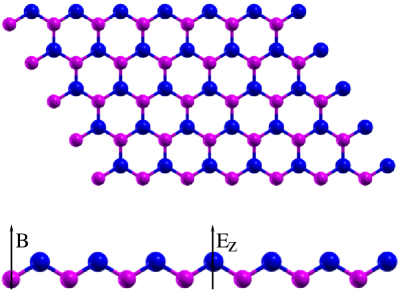
Silicene is a monolayer of silicon 16 ; 17 (isostructural to graphene) with very strong SOI. It has a buckled honeycomb structure, see Fig. 1, where the charge carriers behave like massless Dirac fermions 18 . This breaks the inversion symmetry and gives rise to a quantum valley Hall effect 27 . Experimental realizations of silicene sheets 18 ; 19 ; 20 and ribbons 21 ; 22 have been demonstrated by synthesis on metal surfaces. It is believed that silicene opens new opportunities for electrically tunable electronic devices 23 . Although graphene possesses extraordinary properties, its application in device fabrication is limited by the zero band gap and the difficulty to tune the Dirac particles electrically. Moreover, even if a band gap could be introduced by chemical doping, it would be incompatible with existing nanoelectronics. In the desire to overcome this limitation, the buckling in silicene offers a solution for manipulating the particle dispersion to achieve an electrically tunable band gap. In addition to the latter, silicene has a relatively large band gap of 1.55 meV 24 induced by intrinsic SOI, which provides a mass to the Dirac fermions. This mass can be controlled experimentally by an external perpendicular electric field.
In the light of the above discussion, silicene is likely to show significant signatures of QHE as well as TI quantum phase transitions. The QHE is the fundamental transport process under an external perpendicular magnetic field. For intrinsic SOI and an external perpendicular electric field, we show in the following that the quantum phase transition from a two dimensional TI to a trivial insulator is accompanied by quenching of the QHE and onset of a valley quantum Hall effect (VQHE), providing a tool to experimentally tune the topological state of silicene. We use the Kubo formalism to discuss the Hall conductivity and address the longitudinal conductivity for elastic impurity scattering in the first Born approximation.
Results
We model silicene by an effective Hamiltonian in the xy-plane. An external magnetic field (0, 0, ) is applied perpendicular to the silicene sheet, taking into account SOI and electric field 27 ; 25 ; 26 . Dirac fermions in buckled silicene obey the two-dimensional graphene-like Hamiltonian
| (1) |
Here, denotes , , where is the uniform electric field applied perpendicular to the silicene sheet, with Å. In addition, (, , ) is the vector of Pauli matrices and denotes the Fermi velocity of the Dirac fermions. Spin up () and down () is represented by and , respectively. Moreover, is the two dimensional canonical momentum with vector potential and is the speed of light. Using the Landau gauge with vector potential (0, , 0) and diagonalizing the Hamiltonian given in Eq. (1) we obtain the eigenvalues
| (2) | |||||
Here, denotes the electron/hole band, , and is an integer. The eigenfunctions for the point can be obtained by exchanging the electron and hole eigenstates in the point solution with interchanged by . For more details see the supplementary information (Section I).
In the presence of a magnetic field there are two contributions to the magnetoconductivity: the Hall and longitudinal conductivities. The latter is the localized state contribution responsible for Shubnikov de Haas (SdH) oscillations. The Hall conductivity is the non-diagonal contribution. In order to calculate the electrical conductivity in the presence of SOI, an electric field, and a perpendicular magnetic field, we employ the general Liouville equation 28 . The Hall conductivity is obtained from the non-diagonal elements of the conductivity tensor as 29 ; 30
| (3) |
Solving and simplifying, see the supplementary information (Section II), yields in the limit of zero temperature
| (4) |
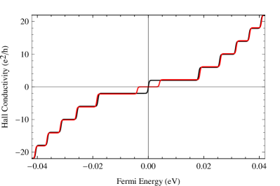
with . This result is identical to the integer quantum Hall effect in graphene 2 ; 3 ; 29 ; 30 for , where the plateaus appear at , as shown in Fig. 2. For and there is a plateau at the charge neutrality point (CNP) in Fig. 2(top), which confirms that silicene is gapped due to strong SOI. The parameters used in Figs. 2 to 5 are m-2, eV/T, m2, m-1, m/s, and .
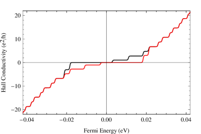
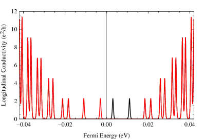
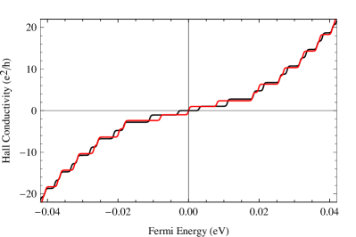
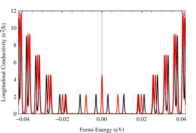
Furthermore, we show the Hall conductivity in Fig. 3(top) as a function of the Fermi energy for fixed values of the magnetic field and temperature. We find plateaus in the Hall conductivity at for both valleys in the limit of large electric field energy (). The total Hall conductivity of the K and K′ valleys together for and is presented in Fig. 4(top). The extra plateaus at 0 and reflect the quantum phase transition which lifts the four-fold degeneracy of the Landau level (LL). This is not possible in graphene. Moreover, for meV we find a single peak at the CNP with electron hole symmetry and plateaus at . This corresponds to the semimetallic state of the system 31 . There are three major differences between silicene and graphene: First, the electrical effects due to buckling polarize all LLs. Second, the SOI is much stronger. Third, the spin and valley degeneracy factor 4 is missing in the prefactor of Eq. (4). This demonstrates that the surface states of the silicene TI have a strong spin texture structure, which is distinct from the ideal Dirac fermions in graphene and results in a different quantum Hall conductivity. We note that the LLs are still doubly degenerate, consisting of spin up and down states from different valleys. The factor of 2 in the prefactor of Eq. (4) is due to this degeneracy.
We argue that silicene undergoes a quantum phase transition from a trivial insulator, in which the Hall conductivity at the CNP is zero, to a Hall insulator, in which the Hall conductivity equals . The transition happens when and is associated with a non-analytic contribution to the conductivity from the LL. The transition is the result of a change in the character of the LL, see Eq. (2), which happens in each valley independently. For one of the sublevels is electron-like and the other hole-like in both valleys. When the electric field energy exceeds the SOI, both sublevels are electron-like for the K valley and hole-like for the K′ valley. The Hall conductivity in Eq. (4) evaluated for zero Fermi energy jumps from 0 (, ) to () by tuning the electric field.
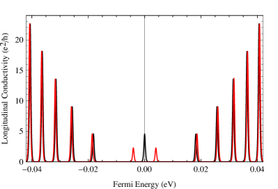
To obtain the longitudinal conductivity, we assume that the electrons are elastically scattered by randomly distributed charged impurities, as it has been shown that charged impurities play the key role in the transport in silicene near the Dirac point. This type of scattering is dominant at low temperature. If there is no spin degeneracy, the longitudinal conductivity is given by 28 ; 29 ; 30
| (5) |
Here, is the Fermi Dirac distribution function, with for elastic scattering, is the Boltzmann constant, and is the chemical potential. is the transmission rate between the one-electron states and , and is the charge of the electron. Conduction occurs by transitions through spatially separated states from to , where . The londitudinal conductivity arises as a result of migration of the cyclotron orbit due to scattering by charged impurities. A detailed derivation is given in the supplementary information (Section III).
In general, the oscillatory part of the longitudinal conductivity in Eq. (5) is expressed as
| (6) |
A closer analytical examination of this result establishes an oscillation with the SdH frequency due to the distribution function entering the expression. For we have a symmetric electron-hole spectrum of the magnetoconductivity with a single peak at the CNP, see Fig. 2(bottom). This situation is the same as for the Dirac fermions in graphene 2 ; 3 ; 29 ; 30 . We obtain a gap at the CNP for and with electron-hole symmetry. For , silicene undergoes a quantum phase transition at the CNP and a well resolved splitting of the SdH oscillations appears. Figure 3(bottom) reveals an oscillatory behavior with the period of the SdH oscillations for the K valley (black line) and the K′ valley (red line) for . This non-trivial behavior is due to the interplay of SOI and electric field, and is highlighted in Fig. 3(bottom). The splitted peak is shifted to the electron and hole region for the K and K′ valley, respectively, when the electric field energy grows relative to the SOI energy. This shift of the LL is consistent with the energy spectrum in Eq. (2). In effect, the longitudinal conductivity at the CNP passes from a minimum to a maximum by tuning the electric field, i.e., the system undergoes a transition from a trivial insulator to a Hall insulator. The behaviour can be characterized as a quantum phase transition. For Eq. (6) gives in the limit of low temperature or high magnetic field , which is consistent with the eigenenergy spectrum of Eq. (2). This fact clearly indicates a lifting of the four-fold degeneracy of the LL and a quantum phase transition at the CNP.
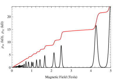
The total Hall (top) and longitudinal (bottom) conductivities of both valleys together are addressed in Fig. 4. For , we see a splitting of the LL into three peaks, one at the CNP and two with electron-hole symmetry. The energy gap between the spin up bands closes, while the spin down bands maintain a gap. This situation corresponds to the semimetallic state of silicene 31 . To observe the effect experimentally, the temperature broadening of the LLs must be less than the SOI energy, which can be achieved at low temperature. Finally, we show the total Hall and longitudinal resistivities as a function of the magnetic field in Fig. 5. These results refer to the regime with meV and meV to cleary see the VQHE. We find that steps between the plateaus coincide with sharp peaks of the longitudinal resistivity. For high magnetic field, we find a significant splitting of the Hall plateaus and the corresponding peaks in the longitudinal resistivity. In contrast, for low magnetic field, we observe a beating pattern of the SdH oscillations due to the energy difference between SOI and electric field for the spin up and down states. The electric field breaks the inversion symmetry and the surface Dirac fermions acquire a mass due to both the SOI and electric field.
Discussion
The following conclusions apply to both conductivities: (i) For there is a minimum at the CNP due to splitting of the LL in two sublevels because of the SOI. (ii) For there is a peak at the CNP with electron-hole symmetry. This corresponds to the semimetallic state. (iii) For we have a splitting of the LL into four sublevels (two peaks in the electron and two in the hole region) with a gap at the CNP. All other LLs are also split. We call this a quantum phase transition due to the shifting of electron and hole peaks in the K and K′ valley, respectively. The four-fold degeneracy of the LL is fully resolved and all other LLs split into two two-fold degenerate sublevels as the spin up states of one valley coincide with the spin down states of the other valley. This property distinguishes silicene from graphene 2 ; 3 ; 29 ; 30 .
Our analytical calculations for the Hall and longitudinal conductivities in silicene include an electric field to model electrical tuning in nanoelectronic applications. We have shown that the Hall conductivity is an integer multiple of with plateaus at for , which is a clear signature of the VQHE. The Hall conductivity jumps from 0 to 1 at the critical electric field of the level crossing. This reflects the transition from a trivial insulator to a Hall insulator at the CNP. The derived results also apply to isostructural germanene, for which the SOI is even stronger ( meV with Å). Experimentally, the best way to see the QHE and VQHE is to measure the Hall conductivity as a function of the gate voltage which tunes the chemical potential. In silicene and germanene the temperature will not affect the Hall plateau as the SOI and electric field are strong. We have shown that the energy splitting due to and leads to unconventional plateaus in the QHE and VQHE with a quantum phase transition at the CNP. Thus, the QHE, the VQHE, and the topological insulating states in silicene and germanene can be observed and tuned experimentally at finite temperature. The fact that the splitting due to the SOI can be controlled by an external electric field (gate voltage) is of great significance for electrically tunable spintronic devices. Our predictions represent a milestone for spin and valley electronics as silicene enables such devices, compatible with the existing technology.
Acknowledgements
We acknowledge fruitful discussions with M. Ezawa.
Author contributions
MT performed the calculations. Both authors wrote the manuscript.
Additional Information
Competing Financial Interests
The authors declare no competing financial interests.
References
- (1) K. v. Klitzing, G. Dorda, and M. Pepper, Phys. Rev. Lett. 45, 494 (1980).
- (2) K. S. Novoselov, A. K. Geim, S. V. Morozov, D. Jiang, M. I. Katsnelson, I. V. Grigorieva, S. V. Dubonos, and A. A. Firsov, Nature 438, 197 (2005).
- (3) Y. B. Zhang, Y. W. Tan, H. L. Stormer, and P. Kim, Nature 438, 201 (2005).
- (4) A. K. Geim, Science 324, 1530 (2009).
- (5) A. H. Castro Neto, F. Guinea, N. M. R. Peres, K. S. Novoselov, and A. K. Geim, Rev. Mod. Phys. 81, 109 (2009).
- (6) C. L. Kane and E. J. Mele, Phys. Rev. Lett. 95, 146802 (2005).
- (7) C. L. Kane and E. J. Mele, Phys. Rev. Lett. 95, 226801 (2005).
- (8) B. A. Bernevig, T. L. Hughes, and S. C. Zhang, Science 314, 1757 (2006).
- (9) N. A. Sinitsyn, J. E. Hill, H. Min, J. Sinova, and A. H. MacDonald, Phys. Rev. Lett. 97, 106804 (2006).
- (10) S. Murakami, Phys. Rev. Lett. 97, 236805 (2006).
- (11) M. König, S. Wiedmann, C. Brüne, A. Roth, H. Buhmann, L. W. Molenkamp, X. L. Qi, and S. C. Zhang, Science 318, 766 (2007).
- (12) C. X. Liu, T. L. Hughes, X. L. Qi, K. Wang, and S. C. Zhang, Phys. Rev. Lett. 100, 236601 (2008).
- (13) D. Pesin and A. H. MacDonald, Nat. Mat. 11, 409 (2012).
- (14) A. Rycerz, J. Tworzydlo, and C. W. J. Beenakker, Nat. Phys. 3, 172 (2007).
- (15) D. Xiao, W. Yao, and Q. Niu, Phys. Rev. Lett. 99, 236809 (2007).
- (16) K. Takeda and K. Shiraishi, Phys. Rev. B 50, 14916 (1994).
- (17) G. G. Guzmán-Verri and L. C. Lew Yan Voon, Phys. Rev. B 76, 075131 (2007).
- (18) P. Vogt, P. D. Padova, C. Quaresima, J. Avila, E. Frantzeskakis, M. C. Asensio, A. Resta, B. Ealet, and G. L. Lay, Phys. Rev. Lett. 108, 155501 (2012).
- (19) M. Tahir and U. Schwingenschlögl, arXiv:1206.3650v1.
- (20) B. Lalmi, H. Oughaddou, H. Enriquez, A. Kara, S. Vizzini, B. Ealet, and B. Aufray, Appl. Phys. Lett. 97, 223109 (2010).
- (21) A. Fleurence, R. Friedlein, T. Ozaki, H. Kawai, Y. Wang, and Y. Y. Takamura, Phys. Rev. Lett. 108, 245501 (2012).
- (22) B. Aufray, A. Kara, S. Vizzini, H. Oughaddou, C. Léandri, B. Ealet, and G. L. Lay, Appl. Phys. Lett. 96, 183102 (2010).
- (23) P. E. Padova, C. Quaresima, C. Ottaviani, P. M. Sheverdyaeva, P. Moras, C. Carbone, D. Topwal, B. Olivieri, A. Kara, H. Oughaddou, B. Aufray, and G. L. Lay, Appl. Phys. Lett. 96, 261905 (2010).
- (24) N. D. Drummond, V. Zólyomi, and V. I. Fal′ko, Phys. Rev. B 85, 075423 (2012).
- (25) C. C. Liu, W. Feng, and Y. Yao, Phys. Rev. Lett. 107, 076802 (2011).
- (26) C. C. Liu, H. Jiang, and Y. Yao, Phys. Rev. B 84, 195430 (2011).
- (27) M. Ezawa, J. Phys. Soc. Jpn. 81, 064705 (2012).
- (28) M. Charbonneau, K. M. van Vliet, and P. Vasilopoulos, J. Math. Phys. 23, 318 (1982).
- (29) V. P. Gusynin and S. G. Sharapov, Phys. Rev. Lett. 95, 146801 (2005).
- (30) V. P. Gusynin and S. G. Sharapov, Phys. Rev. B 73, 245411 (2006).
- (31) A. A. Burkov and L. Balents, Phys. Rev. Lett. 107, 127205 (2011), and references therein.